Note : Les descriptions sont présentées dans la langue officielle dans laquelle elles ont été soumises.
~ ~ 3 ~3~
--1
The present invention relates, in general, to modulation and
demodulation techniques and, moxe particularly, to a frequency
shift keying modulation and demodulation technique on a current
loop.
Frequency Shift Keying (FSK) is a form of frequency modulation
commonly used in low-speed modems in which the two states of the
signal are transmitted at two separate frequencies. A 1 is
transmitt~d by a predefined signal frequency (space frequency) and
a 0 is transmitted by another predefined signal frequency (mark
frequency). In noisy environments, it has been found the FSK has
more noise immunity than other forms of modulation, such as
amplitude modulation or phase modulation. In power limited
devices, such as loop transmitters and battery powered devices,
the use of FSK for on-line communication between the 'cransmitter
1~ and another device typically requires a substantial amount of
power due to the numerous circuit elements required to decode and
encode the FSK signals. In order to minimize power usage,
modulation techniques not utilizing frequency shift keying have
been developed, such as that employed in U.S. Patent No. 4,607,247
(Sterling, Jr., et al).
Because of the foregoing, it has become desirable to develop
a frequency shift keying modulation system and demodulation system
which minimizes overall power usage and hardware requirements.
The present invention provides a current loop arrangement
having a power supply for supplying current at various current
levels, a current loop connected to the power supply for carrying
the current levels, means for modulating frequency shift keying
pulses to produce signals having a first predefined frequency and
having a second predefined frequency, and means for connecting
said modulating means to said current loop, said connecting means
permitting the communication of said signals produced by said
modulating means onto said current loop.
In the preferred ~orm, the modulation system includes a
digitally controlled oscillator whose output frequency is
: ; :
: , ~
,
. .
:
--2--
reyulated by the rate of charging and ~ischarginy of a capacitor
within same. A predefined upper frequency (mark frequency) is
determined by the value of a parallel comhination of resistors,
whereas predefined lower frequency (space frequency) ls determined
by the ratio of the resistance of one of the foreyolny resistors
to the sum of the resistances of both resistors. The signal
produced by the diyitally controlled oscillator i5 superimposed
on a current loop.
The invention also provides a current loop arrangement haviny
a powar supply for supplying a current at various current levels,
a current loop connected to the power supply for carryiny the
current levels, said current levels being modulated by frequency
shift keying pulses, means for demodulating said current level to
produce frequency shift keying pulses, and means for connecting
said demodulating means to said current loop.
In the preferred form, the demodulation system includes a
digitally controlled oscillator and a phase comparator
interconnected in a phase-locked loop arrangement. The signal
produced by the comparator is filtered and compared to another
signal to produce an output signal that is the digital
representation of the frequency shift keying siynal superimposed
on the current loop.
The systems of the invention reduce power requirements and the
number of components required as compared with the known systems.
25 BRIEF DESCRIPTION OF THE DRAWINGS
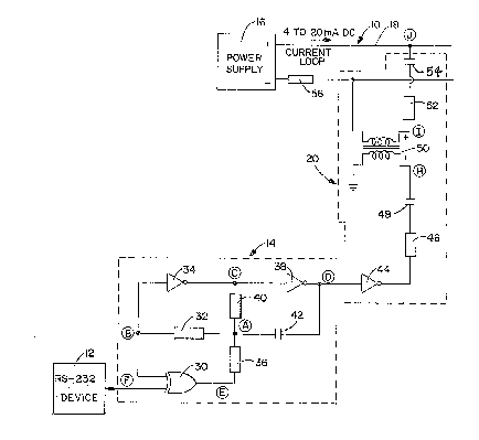
Figure 1 is a schematic drawiny of the frequency shift keying
modulation system of the present invention.
Figure 2 illustrates waveforms at various points within the
modulation system shown in Figure 1.
30 Figure 3 is a schematic drawing of the frequency shift keying
demodulation system of the present invention.
Figure 4 illustrates waveforms at various points within the
demodulation system shown in Figure 3.
'` `' ' ': : '
- ' - ' :
.: . .
.
-,7~
-3-
DESCRlPTION OF TIE PE~I~E'ERREL~ EML~OO~.[~EllT
Referrlng now to the drawings where the illustrations are
for the pu~pose of descrlbing the preEerred ~Inbodllnerlt of the
present inverltion and are not lnterlde~ to LLInlt t~le lnvention
hereto, Figuxe 1 is a schernatic dlagrarn of tlle frecluency shift
keying modulatlon system 10 of -the present inverltiorl. ~l~he system
is comprised oE a transmitting interface device 12,
digitally controlled oscillator 14, a power supply 16 powering a
current loop 18, and a circuit 20 lnterconnecting the digitally
controlled oscillator 14 and the current loop 18.
The interface device 12 is commonly re~exred to as an RS-
232, or the like, and is properly referred to as an Interface
Between Data Terminal Equiplnent and Data Colnmurlication ~quiplnent
Employing Serial Binary Data Intexchange. The interface device
12 generates a supply voltage Vs for one of the two possible
signal states ~space frequency) and a 0 output voltage for the
other signal state (mark frequenc~). The output of the interface
device 12 is connected to an lnput to an OR gate 30 within the
20 digitally controlled oscillator 14. The other input to the OR
gate 30 is connected at point ~ to one side oE a resistor 32 and
to the input to an inverter 34, The output of t~le OR gate 30 ls
connected to a resistor 36 which is connected to the other side
oE resistor 32 at point A. The output of inverter 34 is
connected at point C to the input to an inverter 38 and to one
side of a resistor 40. The other side of resistor 40 is
connected to resistors 32 and 36 at point A. A capacitor 42 is
connected from point A to the output of inverter 3~ (point D)~
The output of inverter 38, which represents the output of the
30 digitally controlled oscillator 14, is connected to the input to
an inverter 44. The output of inverter 44 is connected to a
series combination oE a reslstor 4~ and a capacitor 48 which is
connected to one side of a transformer 50 which is grounded. The
' ~
.
other side oE the trans~ormer 50 ls connected a-ross the current
loo~ 1~ via a resl.stor 52 and a capacl~or 54. 'rl1e current loop
18 includes a resls~or 56 and ls connected to the output oE the
power supply 16 tllat can typica:Lly dr~w a In:Lrl:Llnl~ oE 4 m~ to a
maxilnum of 20 mA.
Operationally, the output voltaye o~ the :interace device
12 controls the frequency of the dlgitally controlled oscillator
14. Re~erring to Figure 2, the output o~ the interface d~vlce
n 12 is shown as waveform F. The other waveforl[ls shown in Flgure 2
represent the vol-tages at varlous polnts within the modulation
system 10 and correspond with the letters silo~n on Flyure 1.
Wlth respect to waveform F, presence of a supply voltage V at
the output of the interface device 12 results ln the dlyitally
lS controlled osclllator 14 producing a predefined upper slgnal
frequency (space frequency), whereas ~voltaye at the output of
the interface device 12 results in the osclllator 14 produclng
l a prede~ined lower signal frequency (mark frequency). When a
suppl~ volta~e Vs exlsts at point F, the OR yate 30 acts as an
20 inverter ~or the signal at point B. The presence of a voltage
at point B, as shown in Figure 2 (point a), causes the voltages
:~3~? at points E and ~ to be O and ~he voltage at point D to be the
~Ij supply voltage Vs~ Inasmuch as OR gate 30 and lnverter 34 have
high input lmpedances, a negligible current flows through
25 resistor 32 and the voltages at points ~ and B are substantially
equal to the supply voltage Vs~ As capacitor 42 starts charging
from point D through resistors 40 and 36 to points C and E,
respectively, the voltage at point A starts decreasing from the
supply voltage Vs toward O volts. When points B and A reach the
30 maximum input voltage for a logic zero trip po:lnt (VIL) o the OR
ga-te 30 and inverter 34, these devices switch causing the
voltages at points C and E to increase to the supply voltage Vs
which, in turn, causes the volta.ge at points B, A and D to
.
' - : -- :' " '
'.~''. ~ "
,
'.'' ', ~ ` .' '
: ' ` ' . ` '
. .
. . : ' - :
~ r~
5~
beco~ne 0. When point D becomes 0 volts, e~pacitor 4Z starts
discharging through resistors 40 and 36, causirlg the voltaye at
point B to start increasing from 0 volts to-,~ards t}le supply
voltage Vs. When point B reaches the minimuIn input voltage for
logic one trip point (VIH) of OR gate 30 and inverter 34, these
devices switch causing the vol-~age a~ points C and E to become 0
and the voltage at points B, A and D to becoIne the supply
volta~3e Vs- Since points E and C are equal at a:Ll tllnes, the
cllarging and discharging kime of capaeltor 42 is proportional to
the parallel combination of resistors 40 and 36. Oscillations
continue at the rate of charging and discharging of capacitor 42~
whicll represents the predefined upper slgnal frequency ~space
frequency), until the input voltage at point F chan~es.
When the output of the lnterface device 12 is 0 volts
~Figure ~, polnt d), then OR gate 30 ae-ts as a non-inverting
buffer for the voltage at polnt B resulting in the output at
point ~ equallLny the input at point B. This condition causes
poin~s C and E to be oE opposite potential at all times~ When
this occurs, the charging and discharging time of capacitor 42
will be proportional to the ratio of the resistance of resistor
to the sum of the resistance of resistors 40 and 36. This
results ln the capacitor 42 charging and discharging at a slower
rate which, in turn, causes oseillatlons to be produeed at a
25 predeflned lower frequëney (mark frequeneyj. Thus, the digitally
controlled oseillator 14 produees an output at point D at a
predefined upper signal frequency when the input at point F is
equal to the supply voltage Vs and produces a predefined lower
signal frequeney when the input at point F is 0 volts.
The output of the digitally eontrolled oscillator 14 drives
the transformer 50 via the inverter 44 r resistor 46 and capacitor
48. The transformer 50 is used to isolate the osci:Llator 14 from
,
.
--6--
the current loop 18, The siynal at polnt ll irl ~i'iyure 1 is
reflected to poin~ I by means oE the transforlrler 50 and is AC
coupled to the current loop 1~ through resist~or 52 and capacitor
5 54. The trans~ormer 50 prevents any DC current ~rom the current
loop from being transmitted to the diyitally controlled
oscillator 14, and vice versa. This perlnits on-line
colnlnunication on the current loop 18 without disturbiny the 4 to
20 mA DC current present thereon.
Referring now to Figure 3, a schelnatic diagram of a
frequency shift keying demodulation system 60 of the present
invention is illustrated. Those components which are similar to
the components utilized within the rnodulation systeln 10 carry
similar reference numerals and will not be discussed in further
15 detail. The demodulation system 60 includes a demodulator 62, a
current 64 interconnecting the demodulator 62 wi-th the current
loop 18, a digitally controlled oscillator 1 4, and a receiving
interface device 66. The current 64 intercol1nects the current
loop 18 with the demodulator 62 by means oE a transformer 68
20 llaving one side connected across the current loop 18 via a
resistor 70 and a capacitor 72. The other side of the
transformer 68 is connected to ground and to a band- pass ~ilter
7~ whose output is connected to one input to an OR gate 76. The
otller input to the OR gate 76 is connected to the output of the
25 inverter 38 within the digitally controlled oscillator 14. The
output of the OR gate 76 is connected to an input to the OR gate
30 within the oscillator 14 and to a resistor 78 whicll i9
connected to one side of a resi9tor 80 atld to yround via a
capacitor 82. The other side of resistor 80 is connected to an
30 input to an OR gate 84 and to the output oE same via a resistor
86. The other input to OR gate 84 is connected to ground. The
output of OR gate 84 is connected to the receiving inter~ace
device 66, which can be a RS-232, or the like.
,. , '
.
'
,` ` ~: ', , ` ,
~7 -
~ s in the prevlous discusslon, the wave~orms at selectedpOirltS OII Figure 3 are shown in Figure ~. Operationally~ a
frequency shift keying slynal on the currellt loop 18 ls
translllltted through the capacltor 72, resistor /~ an(l trarlsforlller
68 to the band-pass filter 74. The ~C coupliny of the
transEormer 68 prevents any DC current ~rom the current loop 18
from passing to the demodulator 62~ The band-pass filter 74
rejects any signal outside the frequency shl~t keying band. The
output of filter 74, shown in Figure 4 as waveform C, is a
digltal representatlon o~ the flltered frequency shift keying
signalO
The system comprised o~ the digitally controlled oscillator
14 and the OR gate 76 is a form of a phase-locked loop. The
signals at points B and C are compaxed by the OR gate 76
producing an output at point A which is translnitted back to the
diyitally controlled oscillator 14 to adjust lts frequency so as
to be the same as the input frequency at point C. In order to
accomplish the foregoing, the duty cycle of the digitally
controlled oscillator 14 varies with the input frequency. A low
input frequency produces an oscillator duty cycle less than 50%
whereas a high inpu~ fre~uency produces an oscillator duty cycle
greater than 50%.
The signal at point D is the average of the slgnal produced
25 at point A filtered by the RC circuit comprised oE resistor 78
and capacitor 82. OR gate 84 acts as a voltage comparator, i.e.,
if the voltage at point D is above Vcc/2, then the voltage at
point F goes high (Flgure 4-waveform F)o However, if the voltage
o~ point D is less than Vccat/2, then the voltac3e at point F goes
low. In essence, the voltage at point F is the dlc31tal
representation of the frequency shlft keying signal arld can be
transmitted to any data terminal equipment (not shown) by the
interface device 66. Resistors 86 and 80 introduce a hysteresis
to OR gate 84 to reduce any jitter when a level transition
35 Occurs.
-'
.;
. -. - ~ .
_~_
The rnajor advantages of the modulatlorl sys~em 10 and the
demodulation system 60 arc the low power requirelnents of these
systems. Such low power requirements can be attributed to the
reduced number of components required within the systerns, the
use o~ CMOS chips where appropriate and the low unlt values for
the capacitors utllized. These systems are also frequency stable
under wide variations in power supply voltage because the input
trip points (V~l and VI~) of the gates are proportional to the
power supply voltage. The foregoin~ advantages perrnit reliable
on-line communication between the low power devices using the
same current loop that carries the 4 to 20 mA DC without
effecting the DC current value~
Certain modifications and ilnprovements will occur to those
skilled in the art upon reading the ioregoing. It should be
understood that all such modification and improvements have been
dele-ted herein ~or the sake of conciseness and readability, but
are properly within the scope of the following claims.
,
., : . .
-, .' ~ ' .,
.
' . : . . ' :, :
. ` .~ ' ' ~.