Note : Les descriptions sont présentées dans la langue officielle dans laquelle elles ont été soumises.
- 20141~L
REFERENCE TO MICROFICHE APPENDIX
Appended to this specification is a microfiche appendix of
an embodiment of the software programming utilized with the
invention. The microfiche appendix consists of one microfiche
page containing a total of 15 frames.
BACKGROUND OF THE INVENTIO~
This invention relates to a touch panel and a method for
controlling same.
Touch panel frames have recently become widely used in
conjunction with video displays such as C~T screens or flat panel
displays. One form of touch panel presently being used includes
a rectangular frame which mounts in front of the display and
which includes a plurality of devices around its perimeter for
emitting energy beams and projecting them across the screen to an
oppositely positioned beam detector. When a stylus or other
foreign object blocks one or more of the beams, an analyzing
circuit senses the blockage and calculates the location of the
blockage on the surface of the screen. This information is then
transferred to a host computer which controls the video display.
Thus, it is possible to use a stylus, or even a person's finger,
to write or mark on the screen.
D;fferent kinds of energy beams have been utilized, but
infrared beams zre commonly used. One problem with the
utilization of infrared beams is thzt am~ient light can sometimes
interfere with the ability of the system to sense blockage of the
particular beams being projected across the screen.
- 2 - *
- 20~41~1
One way of preventing the interference of ambient light is
to cause the infrared beams to be modulated at a particular
frequency so that the electronic circuitry can analyze and sense
the blockage of a beam as it is being projected across the video
screen.
An example of such a device is shown in U.S. Patent
4,868,912. However, the device shown in this patent modulates
the infrared beam with an LED modulator, wh~ch is a separate
electronic device incorporated into the circuit. The LED
modulator generates an analog sine wave signal which is later
converted to a digital signal by other components within the
device .
Therefore, a primary object of the present invention is the
provision of an improved touch panel and method for controlling
the same.
A further object of the present invention is the provision
of an improved touch panel which utilizes a central processor for
modulating the generation of the various infrared beams, rather
than utilizing a separate electrical component for modulating the
beams as is the case in the above Patent 4,868,912.
A further object of the present invention is the provision
of a touch panel a~d method for controll in~ same which permits
the easy adjustment or ~ariance of the particular m~nn~r in which
the light beams are modulated.
A further object of the present invention is the pro~ision
of an i~.p Gved touch panel and method for controlling same which
-- 3 --
- 201~111
utilizes simpler electrical circuitry and fewer electrical
components than in prior devices.
A further ob~ect of the present invention is the provision
of an improved touch panel which uses a central processor capable
of initially generating a digital modulated signal for modulating
the energy beam.
A further object of the present invention is the provision
of an improved touch panel which is economical to manufacture,
durable in use, and efficient in operation.
SUMMARY OF THE I~V~;N ~10N
The touch panel of the present invention includes a
rectangular frame having a plurality of beam emitter-detector
pairs disposed around the perimeter thereof. The emitters
generate a plurality of infrared beams which are directed across
the display panel and which are received by the detectors. The
detectors analyze the light received, and create an electrical
signal which is sent to a comparator. The comparator analyzes
the signal to det~rm;ne whether or not a blockage of the beams
hzs occurred. If a blockage has occurred, the comparator sends a
~lockage signal to a central processing unit which analyzes the
blockage signal and calculates the location of the blockage on
the screen~
The central processor is also connected to the emitter-
detector pairs, and controls the scAnn;~g of the emitter-detector
pairs one at a time. As the sc~nn;ng occurs, the central
processing unit also generates a digital signal which controls
2 ~
the modulation of each emitter as it is activated. The
modulation of this beam is at a freguency which may be varied
according to the choice. Frequencie~ of from between 10
kilohertz and 500 kilohertz will pro~ide satisfactory results.
The preferred frequency is between 60 to 90 kilohertz.
The proce~ing unit is programmed to modulate the frequency
of the light beam as described above. Furthermore, the
particular beam created is in a square wa~e form. That is, the
beam alternates between on and an off condition at a frequency to
be determined by the program within the central processing unit.
Prior devices have been utilized which modulate the light
beams, but these prior de~ices have generated a sine wave form to
the light beam, rather than the sguare wave of the present
invention. Further~ore, the apparatus for modulating the beams
in prior devices has been a separate electrical component as
opposed to the central processing unit of the circuitry. The
program wi~hin the central processing unit of the present
invention controls the modulation rather than hardware as in
prior devices.
BRIEF DESCRIPTION OF TEE DRAWINGS
Fig~re 1 is an exploded perspective ~iew of the touch panel
o~:the present_invent; ~n,
Figure 2 is a sectional view of the-touch panel assembled to
a panel display.
Figure 3 is a block diagram of the touch panel of the
present invention.
20141~1
Figures 4 and 5 are electrical schematic views of the
circuitry of the present invention.
Figure 6 shows the wave form generated by the program within
the central processing unit.
~ igure 7 is an enlarged ~iew taken along line 7-7 of Figure
6.
DESCRIPTION OF THE PREFERRED EMBODIMENT
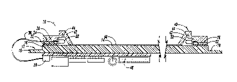
Referring to the drawings, the numeral 10 generally
designates the touch panel assembly of the present invention.
Assembly 10 includes a panel display 12 having a display surface
14, a display frame 16, and a pair of side mounting flanges 18.
Mounting holes 20 extend through the mounting flanges and permit
mounting of the display to a housing or other device to which it
is desired to attach the touch panel.
Secured o~er the frame 16 is an electrically insulati~e
gasket 22, and in facing engagement with gasket 22 is the touch
frame 24. Touch frame 24 includes a rectangular PC board frame
26 having a plurality of bottom LEDs 28 along one side thereof,
and a plurality of right-hand LEDs 30 located on the right-hand
side thereof. The LEDs are directed inwzrdly so that when they
are energized they will project infrared beams across the
inter;or space within frame 24~ A plur~l;ty of top photo-
tra~sducers 32 and left-hand photo-transducers 3~ are mounted on
the top and left-hand side of the frame for recei~ing the beams
from LEDs 28, 30 respectively. Attached to the left-hand side of
the de~ice is a detector cable 36 which is connected to each of
2014~11
the photo-transducers 32, 34. An LED cable 38 is connected to
the bottom of the frame and includes cables leading to each of
the LEDs 28, 30.
Superimposed over the touch frame 24 is a bezel frame 40
having four inwardly canted or beveled lenses 42 behind which are
provided elongated element channels 44. The element channels 44
receive the LEDs 28, 30 and the photo-transducers 32, 34 as
indicated in Figure 2. Thus, the light emanating from the LEDs
28, 30 extends through the lenses 42 and across the screen. A
filter plate 46 is superimposed over the display surface 14 of
display panel 12.
Mounted to the back surface of display panel 12 is a
controller board 48 which includes a plurality of electrical
components thereon to be described hereafter. The various
components are secured together by means of screws 50 which
extend through registered holes in the bezel 40, the touch frame
24, the gasket 22, the display panel 12, and the controller board
48. 3etector cable 36 and LED cable 38 each include a connector
3~ which is adapted to plug into controller ~oard 48 as
illustrated in Figure 2.
Figure 3 illustrates a block diagram showing the ~arious
components on the controller board 48~ These cu~o~ents include
a central processing chip 52. The preferred model for Chip 52 is
manufactured by Motorola under the model number MC68701S. An LED
anode driver 54, and an LED cathode driver 56 are connected to
the LEDs 28, 30 for driving them. The central processing unit is
2~1~111
connected to the cathode driver 56 by a modulation line 58 which
modulates the actuation of the LEDs 28, 30 as will be described
hereinafter. Also contained on the board are a detector decoder
60 and a detector multiplexor 62, each of which is connected to
each of the photo-transducers 32, 34. An amplifier 64 is
connected to the multiplexor 62 and is also connected to a
comparator 66 which in turn is connected to the central
processing unit 52. A transceiver 68 is connected to the central
processing unit and leads to a host computer. The transceiver
permits the host computer either to receive signals from the
central processing unit or to direct signals to the central
processing unit. A reset control 70 is also connected to the
central processing unit for placing the unit in condition to
begin operating. An oscillator or clock circuit 80 is connected
to the central processor 52 in conventional fashion.
Referring to Figure 4, a series of special low value
resistors 82 are included in the circuitry between multiplexor 62
and connector 39. Prior devices have used high value resistors
ha~ing values as high as 1500 ohms for the purpose. However, it
has been found that a superior definition is obtained on the
screen if resistors 82 have a much lower value such as 200 ohms.
The central processing unit 52 is programmed with a program
sim;lAr to the program which is contained with~n the apppn~iy~
The program provides several functions. One of the functions is
to control the scAnn;ng of the anodes and the cathodes so they
are enabled one at a time in a sequential fashion. The program
-- 8 --
201~
stored within the central processing unit 52 also includes a
modulation function which causes modulation of the light signals
generated by each of the LEDs 28, 30 as they are actuated.
Figures 6 and 7 illustrate the signal which is generated by
the program within central processing unit 52. The light signal
is designated by the numeral 72, and includes an actuated portion
74 and a deactuated portion 76. As can be seen in Figure 7, the
actuated portion of signal 72 is modulated into a plurality of
square waves 78 which are intermittently turned to an on and an
off condition. The frequency at which this actuated portion is
modulated may vary substantially without detracting from the
invention, but the preferred range of modulation is between 60
and 90 kilohertz. The modulated portion of the circuit comprises
approximately .8 percent of the entire cycle of the signal 72,
with the rem~in;ng portion of the cycle comprising 99.2 percent
of the period of the cycle. During the deactuated portion 76 of
the signal, the other LEDs 28, 30 are being actuated one at a
time.
The program within the central processing unit 52 also
includes a portion which is capable of receiving signals from the
comparators 66, analyzing those signals, and sending an output
signal through the transceiver 68 to the host computer.
In operation, the central processing unit 52 causes 'he LED
anode driver, 54 and the LED cathode driver 56 to actuate the
various LEDs 28, 30 in a se~uential fashion. The program within
the central processing unit sends a digital modulation siynal
_ g _
2014111
through modulation line 58 so as to modulate the LEDs by turning
the cathodes of the LEDs on and off intermittently, thereby
creating the activated modulated portion 74 of the signal 72, for
each LED.
Simultaneously, the computer enables the photo-transducers
32, 34 in sequential fashion so that one transducer 32, 34 is
actuated simultaneously with a corresponding LED 28, 30. The
light signals detected by the photo-transducers 32, 34 are
converted to electrical signals which are transmitted to the
multiplexor 62 and from the multiplexor 62 to the amplifier 64
and the comparator 66. The comparator compares the signal
received from the photo-transducers to a predetermined signal
characteristic to deterri~ whether or not the signal represents
a blockage of the light beam across the panel 14 of the ~ideo
display. If a blockage occurs, the comparator detects such
signal from the characteristic of the signal sent to it from
amplifier 64. The comparator then sends a blockage signal to the
central processing unit 52. This blockage signal tells the
central processing unit 52 that a blockage has occurred. The
program within the central processing unit 52 then calculates the
location of the blockage by analyzing the location of the blocked
intersecting light ~eams which are emanated from LEDs 28, 30.
The central processing unit then sends an output signal to the
host computer.
~ y modulating the light output of the LEDs, it is possible
to create a signal which is easily discriminated from and
-- 10 --
2014~ 1
distinguished from the signals created by ambient light. Ambient
light will ~e detected by the photo-transducers, but the
frequency of the modulated portion of the light signal is easily
distinguished by the comparator 66, thereby minimizing any errors
caused by ambient light.
The advantage of modulating the light signal with the
central processing unit is that 8 separate component for creating
a modulated signal is not required in the circuit. Furthermore,
the specific timing of the light signal can be more easily
controlled by the digital modulating signal generated by the
central processing unit, and the modulation of the signal can be
easily changed by reprogramming the central processing unit. The
signal sent to the decoder drivers is a digital signal rather
than an analog signal as is the case with hardware driven
signals. This permits greater precision, and permits the
amplification of the modulated signal by the amplifier 64 so as
to sive a good ratio of the modulated signal to outside noise
created by ambient light. Consequently, very good discrimination
can be achieved. Thus, it can be seen that the device
accomplishes at least all of its stated objectives.