Note : Les descriptions sont présentées dans la langue officielle dans laquelle elles ont été soumises.
SgOOll
-- 1 --
201453~
BACKGROUND OF THE INVENTlON
1. Field of the invention:
This invention relates to an apparatus for
recordlng and reproducing information on and rom an
optical disk using an optical beam, ~nd on an optical
disk for storing information usefu} i~ such ~n
apparPtus. In the speci~lcation and accompanying
claims, the term "an optlcal dl~k" includes an optical
;v dl5~ in ~hirh infor~atLon cannot be r~rLt~ e. g ., a
so-called compact dlsk) and also that in which
information can be rew~ltten (e.g., a magnetooptical
disk), and the term "an apparatus for recording and
reproducing inform~tlon" means an apparatus which can
record and/or reproducing informstion on and from an
optlcal d~sk.
2. Descrlption of the prior art:
In an apparatus for recording and reproducing
information on and from an optical disk using an
optical beam, tracking servo control is performed so
that an optical beam such as a laser beam accura~ely
tL-C~Y ~-~coraing ~racks preformed in ~he optlcal diSk.
In order to perform the tracking servo control, the
continuous tracking servo method is widely employed
which usPs servo control signals obtained from guiding
grooves or data pits preformatted in an optical dis~
for guidlng a l~ger beam along the recor~lng trac~s.
An optic~i aisk u-~ed in~~ne conllnuous servo
method has preformed continuous grooves or data pit
rows so th~t the servo control signal can be easily
obtained from the grooves or pit rows independently of
-- . . - . _
. ~
S90011
- 2 - 2014535
the data recording density or recording method.
~herefore, this method can be applied to optical disks
with varlous formats.
When using an optical disk on whlch data is
recorded based on varia~ions ln the reflectivlty of the
recording medium or the presence and absence of pits,
however, the continuous æervo method does suffer from
deterioration of the servo cont~ol slgnal obtained from
the grooves or pit rows near the recording areas, due
to the effect of the recorded signal. Furthermore, the
quality of the servo control signal tends to be
affected by slight dimensional inaccuracies such as
shape errors in the guide grooves. Therefore, it is
difficult to obtain compatibllity between various disk
types.
As another method for performing the tracking
servo control, the sample servo method is employe~
~0 which uses a tracking servo contro~ si~nal ob~ained
from servo bytes pre~ormatted in sampling areas which
are formed locally on the optical disk. In the sample
servo method, a phase lock loop (PLL) circuit ~enerates
- a reference clock signal in synchronization with the
timing with which an optical beam passes the servo
bytes. Based on this reference clock signal, a
tracking servo control si~nal is o~tained from the
servo bytes, and the timing with which the data signal
is written and/or read is controlled.
In the sample servo method, the samplin~
areas are completely sepsrated from the areas in which
data is recorded, and therefore the tracking servo
-
S~0011
20~453~
control slgnal is not affected by the recording signal
and a tracking servo control signal of high qual$ty can
~e easily obtained. Furthermore, the formation of
sa~pling areas speciallzed for the tracklng servo
control allows the apparatus to use a relatively simple
detection means, result~ ng ln thAt the sample servo
method can offer a wider range of disk compatlbility
than the contin~ous servo method.
When a ~OCU8 ser~o control is per~ormed
ag2inst ~n optical disk having gu~de grooves in the
astigmatic method, the presence of the guide groo~es
may cause a shadow to form in a beam spot on an optical
detector, thereby necessitating the precise posltioning
of the optical detector. Since it is not necessary to
form guide grooves in an optical dlsk used in the
sample servo method, in contrast, such a shadow does
not form even when a focus servo control is conducted.
Thls results in that the servo control can be
~0 accurately executed without excessively accurate
positioning of an optical detector. Therefore, the
sample servo method offers advantages such as reduced
steps in the assembly of the detector and an i~proved
yleld of an apparatus.
~5
Generally, an optical disk is driven under
either the constant angular velocity (CAV) control in
which the rotational velocity of the disk is controlled
so that its angular velocity is kept constant, or the
constant linear velocity ( CLV ) control in which the
rotational velocity of the dlsk is controlled so that
the ~peed of the optical beam spot with respect to the
optical disk (i.e., the linear velocity) is maintained
S90011
- 4 -
201~53S
constant.
Whlle the CAV control is slmple since the
rotational velocity i8 kept constant irrespect~ve of
the irradiat$on posltlon of the optical beam on the
optical dlsk, the CAV control lnvolves a dlsadvantage
in that the recording denslty at the portion nearer the
outer circumference of the disk becomes smaller, thus
reduc$ng the storage capacity of the disk as 8 whole.
In the CLV control, on the other hand, the
storage capacity can be essily lncreased, but the
rota~ional veloclty of t~e optical disk must ~e v~ied
in accordance with the chsnge of the radia} position of
the optical beam spot on the op~ical disk. Moreover
the extra time required for stabilizing the rotational
velocity makes the access time longer.
To tackle these problems, the modulate-
constant angular veloc~ty (M-CAV) control has been
proposed in which the rotat~onal velocity of the
optlcal disk is kept constant, the recording area of
the disk is divlded into a plurality of blocks
comprlsing multiple tracks, and information is written
and/or read using a clock signal having a higher
frequency in the more ~uter block. According to this
M-CAV control, it ls possible to avoid the increa~e in
the access tlme caused by the change of the rotational
velocity, and in addition, the linear recording density
near the outer circumference of the optical disk is not
reduced, so the storage capacity can be easily
increased.
S9001 1
- 5 - 2014~3~
However, in the M-CAV control, it ls difficult
to employ the sample servo method which has various
advantages as described above, because of the reasons
mentioned ~elow.
That is, in the M-CAY control, the period wlth
whlch the optical beam passes a servo byte changes with
each block. Therefore, when a sample servo method is
used, each tlme the opt~cal beam moves in the radial
direction of the optical disk and enters into another
block, the tracking contro~ cannot be correctly
perormed untll the PLL clrcuit is pulled again into
synchronism.
In the sample servo ~ethod, comparison pulses
input to the PLL circuit per unit time is small in
number so that, if the period with which the optical
beam passes the servo b~te changes greatly, the
response time is prolonged until the PLL circuit is
pulled again into synchronization to generate a stable
reference c~ock signal. Consequently, even though the
M-CAV control method does not reguire the change of the
rotational velocity of the optical disk, it does result
ln longer access times.
When performlng the M-CAV control ln the sample
servo method, therefore, it is difficult to shorten the
overall access tlme wh~le increasing the storage
capaclty of an optlcal dlsk.
-- SgOOll
- 6 -
20I4535
SUMMA~ OF THE INVENTION
Accordlng to the invention, an apparatus for
recording and reproduc~ng information on and from an
S optical disk, using at le~st one optical beam and a
reference clock signal, said optical d~sk comprising
recording tracks which are dlvided lnto a plurality of
blocks, said blocks being concentrically arranged along
the radial direction i8 provided, which overcomes the
above-dlscussed and numerous other disadvantages and
deficlencies of the p~ior art, the appar~tus
comprising: a block ~udglng mea~s for judgin~ one of
said blocks that said one block is currently impinged
by said optical beam; a clock signal generating means
for generat~ng a plurality of clock signals which are
different ~n ~requency from each other: and a clock
signal selecting means for selec~ing one of qaid cloc~
slgnals as said reference clock signal, on the basis of
the judgment o~ s~id block ~udging means.
In a preferred embodiment, the apparatus
further comprises a mo~her clock signal generating
means for generating a mother clock signal, said mother
clock signal being supplied to said clock signal
generating means.
In a preferred embodiment, the mother clock
signal generating means is a phase lock loop circuit.
In a preferred embodiment, the clock signal
generating means comprises a plurality of frequency
divlders for dividi~g said mother clock signal, the
outputs of said frequency divlders being supplied t~
sgll2~I~535
said clock signal selecting means as said clock
signals.
In a preferred embodiment, the apparatus
further comprises a reset mean~ for resetting said
~requency dividers.
In a preferred embodiment, the apparatus
further comprises a driving means for rotating said
optical disk at a predetermined angular velocity.
According to the invention, an optical disk
for storing information is provided, comprising a
plurality of blocks which are separated concentrically
in the radial direction, each of said blocks including
at least one recording ~racks elongating tangentially,
each of sald recording tracks comprising a plurality of
segments, each of said segments includlng a sampling
area and a data region for storing information, said
sampling area containing preformatted servo bytes, each
of segments of tracks ln the same block having the same
central angle, the number of segments included in one
track belong$ng to an outer block be~ng greater than
that of segments included ln one track belonging to an
inner block.
In a preferred embodiment, the mean length of
segments belonging to one of said blocks ls
substantlally the same as the mean lengths of segments
~elonging to other blocks.
In a preferred embodiment, one of said
sampling areas in each said tracks is posit~oned on the
_r :
S90011
- 8 -
2014535
same radlus of sald optlcsl dlsk.
In a preferred e~bodiment, two or more of
said sampling areas in each sald tracks are positioned
respzctively on two or more radii of said optical disk.
Thufi, the inventlon descrlbed hereln makes
possible the o~ectives of:
(1~ providlng an apparatus for recording and
reproduclng lnformation on and from an optlcal disk
which can increase the storage capacity of the optical
disk and prevent the lncrease of the overall access
time even when the M-~AV oontrol ls performed in ~he
1~ sample servo method,
(2) providing an apparatus for record$ng and
reproducing $nformation on and from an optical disk in
which the re~erence clock signal can be quickly
stabilized after ~he optical beam ~umps from one block
of the optical dlsk to another block;
(3) providlng an apparatus for recording and
reproducing information on and from an optical ~isk ln
which the servo control and the information
reproduction and/or record can be quickly resumed after
the optical beam ~umps from one block of the optical
disk to another block; and
(4~ providing an optical dis~ which can be
use~ under the M-CAV con~rol in the sample servo
method, with increasing the storage capacity of the
optical d$sk and preventing the increase of the overall
S90011
- 9 -
201~53~
~cc~ss time.
By means of the above configuration, after
the optical beam moves or ~umps from a block to another
block in the radlal direction of the optical disk, the
new block currently being irradizted ~y the optical
beam ls rapldly discrlminated by the block ~udging
means. Hereinafter, ~uch 2 block currently irradiated
by the optical beam is referred to as "a current
block". Then, the clock slgnal selecting means selects
the clock si~nal with the frequency corresponding to
the current block among the clock signals ~enerated by
the clock signal ~enerating means, based on the signal
from the block juds~ng mesns .
1~
That ls, even when the optical beam moves to
another block, a stabi~zed reference clock signal can
be obt~ne~ in a short t$me, so that the servo c~ntr~i
and the wrlting and/or r~Ad~g of information can be
resumed quickly. Therefore, even if the linear
recording d~nsity ne~r the outer e~se of the disk is
increased by performing the M-CAV control while using
the sample servo method, the overall access time is not
increased.
BRIEF DESCRIPTION O~ THE DRAWINGS
This inventlon may be better understood and
its numerous objects and advantages will become appar-
ent to those skilled in the art by reference to theaccompanying drawings as follows:
S9~011
lo - 2 ~ 3 5
Flgure 1 is a block diagram showlng an
apparatus accordlng to the invention.
Figure 2 illustrates an optical dis~
according to the invention.
Figure 3 ls a diagram showing diagram-
matically the structure of tracks formed ln the optical
disk of Figure 2.
Figure 4 i~ a tlming chart of the
synchron~zing pulse signal produced in the apparatus of
Figure 1.
Flgure 5 is a block diagram showing a block
~udglng unit used in the apparatus of Figure 1.
Figure 6 is a timing chart lllustrsting the
operation of the judging unit of Figure 5.
DESCRIPTION OF TRE ~K~RKED EMBODIM~NTS
Figure 2 shows an optical disk accordlng to
the invention. In the optical disk 11 of Flgure 2, the
recording area is divided into three blocks 14, 15 and
16 each having a plurality of concentric tracks 12.
Namely, tracks 12 formed between radii Rl - R2
constitute the f~rst block 14. Likewlse, tracks 12
formed between radii R2 - R3 and between R3 - R4
constitute the second and third bloc~s 15 and 16,
respectively (R4 > R3 > R2 ~ Rl~.
~ - . ~ - -
201453S
-
S90011
Each track 12 is divided into segments 13
each comprising a series zrrangement of a sampling
area 13a for generatlng the servo slgnal and a dat~
area 13b for recording data. As shown in Figure 3, the
sampllng ~re~s 13a ha~ ~ pr2f~r~a~ed 3~r~e byt~
consisting of wobbled pits 21 for generating the
tracklng signal, and a synchronizing p~t 22 for
generating the synchronizing pulse. The tracking
signal is used as the servo control signal. In the
data areas 13b, data pits ~3 for recordlng information
are for~ed ~y a suitable ~neans such ag engra~ed ~its
magnetically inverted patterns, etc.- The wobbled
pits 21 and synchronizing pits 22 are positioned
according to the international standard ISO-DP9171-2.
In one block, the nu~h~rs of the segments 13
included in each of the tr~cks 12 are identical with
each other. That is, in the same block, the
segments 13 have the seme central anyle, so that the
~eriod with wh~ch the samplin~ aress 13a are irradiated
by the optical besm ~s the same for any track in the
same block when the opt~cal disk ll is rotated at a
constant angular velocity.
In contrast, the number of the segments 13
belonging to one of the blocks differs from that of the
segments 13 belonging to another of the blocks. More
specifically, the num~ers of the segments 13 are set so
that tracks 12 in ~he outer blocks ha~e more segments
(i.e., the number of the segments in the block 16 is
~r~at~ t~zn that in the block 14). In other words,
the mean length of the segments 13 belonging to one of
the blocks 14 - 16 i8 substantially the s~me as ~hat of
2014535
S90011
- 12 -
the segments belonging to other one of the blocks 14 -
16, so that the linear recordlng denslty is
approxlmstely constsnt among the blocks 14 - 16.
In the embodimen~, the positions of the
segments 13 are set ln such a manner that the sampling
areas 13a of one of the segments 13 in each of the
tracks 12 ls positioned on the same or common radius A,
~hereby enabling the synchronization between the
b}ocks 14 - 16 to ~e easily conducted. According to
this arrangement, moreover, the synchronizing pi~s 22
can be readily detected even when the optlcaL beam is
traversing the track~ ~2.
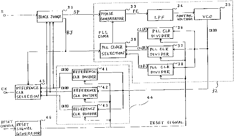
Figure 1 shows an apparatus according to the
invention which can r~ d and reproduce information on
and from the above-descr~bed optical disk 11. The
apparatus of Figure 1 comprises a block judging
unit ~1, a PLL cirCuit 32, a clock signal generator 44,
a reference clock si~nal selection unit 45, and a reset
signal generator 46. The P~L ci~cuit 32 includes z
phase comparatox 33, a low-pass filter 34, a voltage
controlled oscillator (VCO) 35, three PLL clock signal
frequency div~ders 36, 37 and 38, and a ~LL clock
signsl selector 3g. The clock signal generator 4~ has
three reference clock æignal frequency dividers 41, 42
and 43.
The optical disk 11 is mounted on the
apparatus, and scanned by an op~içal beam emitted from
a semiconductor laser device (not shown) while be~ng
rotated at a predetermined constant angular veloc~ty by
a suitable driving device (not shown ) . The optical
201453~
S90011
- 13 -
besm ls reflected ~rom the wobbled pits 21,
synchronizln5 p~ts 22 and data pits 23 of the optical
disk 11. The reflected beams are detected to obtain a
reproduced signal S from the optical disk. The means
for per~ormlng the CAV control and the manner of
obtainlng the reproduced signal is well known in the
art, and therefo~e the~r detailed description is
omitted.
The reproduced signal S ls supplied to the
block Judglng unit 31. The ~lock Judging unit 31 also
receives clock signals CK~A), CK(B) and CK(C) from the
reference clock signal frequency dividers 41 - 43. The
block judging unit 31 produce~ a synchronizing pulse
signal SP and 2 block Judging signal BJ. The
synchronizing pulse slgnal SP is input to the phase
comparator 33 of the PLL c~rcuit 32. The phase
c~parator 33 compares the phass o~ the synchronizlng
pulse signal SP wlth that of a PLL clock signal input
from the PLL C7 ock signal selector 3g, and outputs a
phase error signal PE. The phase error signal PE is
input to ~he low-pass filter 34 which in turn outputs a
control voltage having a level corresponding to the
phase difference between the synchronizing pulse
signal SP and the input PLL clock signal.
The control voltage is input to the VCO 35
which generates a mother clock signal C~(M) wi~h a
frequency corresponding to the level of the input
control voltage and synchron~zed with the synchronizing
p~lse signal SP. The mother clock B~ gnal CK(M) is
supplied to the PLL clock signal frequency
dividers 36 - 38 and ~lso ~o the re~erence clock signal
- - - 2014535
S900 1 1
- 14 -
fre~uency dividers 41 - 43 of the clock signal
gensr~tor 44.
The P~L clock signal frequency divlders 36 -
3B divide the mother clock signal CR(M) to respectively
generate clock slgnals C~(A), C~(B) and CL(C). Each of
the clock signals CL(A) - CL(C) has a frequency
approximately e~ual to that of the synchronizin~ pulse
signal SP whlch is produGed from the block ~udging
unit 31 when the corresponding one of the blocks 14 -
16 of the optical disk 11 ls irradiated by the optical
~eam. The clock signals CL~A) - CL(C) are input to the
PLL cloc~ slgnal selector 39. The PLL clock signal
selector 39 selects one of the cloc~ signals CL~A) -
CL(C~ on the basis of the block judging signal BJout~ut from the block Judging unlt 31, and then sends
out the selecte~ clock signal to the phase
comparator 33 as the PLL clock signal.
As mentioned above, the mother clock
signal CK(M) is also supplied to the .reference clock
signal ~requency dividers 41 - 43 of the clock slgnal
generator 44. The frequency dlvideræ 41 - 43 divide
the mother clock signal CK(M) to respectively generate
clock signals CK(A), CK(B) and CK(C). Each of the
clock signals CK(A) - CK(C) has a frequency corre-
sponding to the period with which the sampling
areas l~a in each of the blocks 14 - 16 are irradiated
by the optical beam. The clock signa}s CK(A) - CK(C)
are supplied to the b~ock ~udging unit 31 as mentioned
above, and also to the reference clock signal selection
unit 4~. Among these clock signals CK(A) - CK(C), the
one having the frequency corresponding to the current
201453~
-
S90011
- 15 -
block is selected by the reference clock signsl
selection unlt 45. The selected cloc~ signal is output
2S a referencs clock signal CK which is employed for
performing the servo control, and the record and
reproductlon of information.
The output of the reset signal generator 46
is connected to the PLL clock slgnal fre~uency
dlviders 36 - 38 and to the reference clock signal
fre~uency divlders 41 - 43. When the optical beam
l~radlates one of the segments 13 whlch is positioned
on the radlus A, a control unit (not shown) produces in
a conventional manner a reset control signal, and
supplies it to the reset signal generator 4~. Upon
receiving the reset control signal, the reset sisnal
generator 46 generates a reset signal so that the
counters of the frequency dividers 36 - 38 and 41 - 43
can be reset and the outputs of the frequency dividers
can be synchronized.
The manner of generating the synchronizing
pulse signal SP and the block judging signal BJ in the
block judging unit 3~ will be described wlth reference
- to Figure 5. The block ~udging unit 31 comprises: a
synchronizing pi~ detector 51 to which the reproduced
signal S is input; wlndow generators 52A - 52C which
respectively receive the clock signals CK(A) - CK(C~;
AN~ gates 53A - 53C, an OR gate 54; and a jud~ing
circuit 55.
As shown in Figure 6, the window
generators 52A - 52C, which may be counters, generate
respectively synchronizing plt extracting window
201~535
S90011
- 16 -
signals WA, WB and WC for T sec. when the periods of
time ~A~ TB and ~C have elapsed after the reset
t TA ~ T ~ 'rC, and T~ - TA ~ T, Tc - TB > T ) . In the
embodiment, the synchronizing pulse slgnal SP is
5 supplied also to the window generators 52A - 52C, to
function as a reset signal. The window signals WA - WC
are input respectively to the AND gates 53A - 53C.
The synchronizlng pit detector 51 produces
from the reproduced signal S a synchronizing pit
detection signal DP which indicates that the
synchronizing pit 22 ln ~he current block is irradiated
~y ~he optlcal beam. The synchronizing pit detection
slgnal DP ls input to the AND gates 53A - 5~C. The
outputs DA - DC of the AND gates 53A - 53C are input to
the 0~ gate ~4. When the optical beam irra~iates the
block 14 (i.e., the block 14 is the cu~rent block), the
synchroni~ing pit detectlon signal DP appears at the
timing corresponding to the window signal WA, resulting
in that the output DA of the AND gate 53A becomes HI~H
while the outputs DB and DC of the AND gates 53B and
53C remain LOW. When the optical beam irradiates the
block 15 or 16 (i.e., the bloc~ lS or 16 is the current
~lock), in contra8t, the synchronizing pit detection
signal DP appears at the tlming corresponding to the
window signal WB or WC, as shown by the broken line in
Figure 6, and the output D8 or DC becomes ~IGH. The
output DA $s output from the OR gate 54 as the
synchronizing pulse signal SP.
In this way, ~he synchroniz-ing pul~e
signal SP is obtained in which the timing of ~IGH-
period depends on the current ~lock, as shown in
201~535
-
S90011
- 17 -
Figure 4. That ls, the linear recordlng density of
each track 12 18 ~pproxlmately the same in the
~locks 14 - 16, and the optical disk 11 is rotated
under the CAV control so that the period of the
synchronizing pulse signal SP obtained from an outer
block is shorter than that obtained from an inner
block. Since one sampling area 13a of one of the
segments 13 of each track 12 ls on the same rad~us A,
moreover, the synchronlzing pulse signa~ SP is obtained
with the same tlming once each revolution of the
optlcal disk 11, ~rrespective of the position of the
optical beam (i.e., whichever ~lock i-s the current
block). ~igure 4 shows the synchronizing pulse
slgnals SP obtained from the blocks 14
The outputs DA - DC of the AN~ gates 53A -
~3C are also input to the ~udging clrcuit 5S. The
Judging circuit 55 ~udges that, when the output DA is
HIGH, the block 14 is the current block, and similarly
that, when the output ~B or DC is HIGH, the block 15 or
16 i8 the current block~ Accor~ing to these judgments,
the judging circuit 55 produces the block ~udging
signal BJ indicating the identification of the curren~
block.
The operation of the apparatus of Figure 1
will be described ln more detail. In ~he PLL
circuit 32 which receives the synchronizing pulse
signal SP, the VC0 35 generates the mother cloc~
slgnal CK(M) having a freguency which is an integral
multiple of that of the synchronizing pulse signal SP,
and synchronized with the signal SP. Three clock
signals CL(A) - CL(C) are produced from the mother
~014~35
-
S900~ 1
- 18 -
clork ~3n21 CK~M) ~y the PLL clock ~nal freouencv
divlders 36 - 38. The PLL clock signal selector 39
selects in accordance with the input block ~udging
signal B~ one of the c~ock signals CL~A) - CL(C) which
has the same fre~uency as the synchronizing pulse
signal SP. The selected PLL clock signal is input to
the phase comparator 33. The phase comparator 33
generates the phase error signal PE corresponding to
t~e pllase dl~eren~e between ths in~ut ~LT clnc~ sign~l
and the synchronlzing pulse signal SP. In the VC0 35
to which the control voltage $s supplied from the low-
pass filter 34, the frequency of the~mother clock
slgnal CK(M) is controlled according to the level of
the input con~rol voltage, and then the oscillation
15 frequency of the VCO 35 ls controlled by the control
vol t~gP. S that the abovg-mentioned phase difference
becomas null.
The mother clock signal CK~M) is also
supplled to the clock signal generator 44 from which
the clock signals CK(A) - CK(C) are generated. The
frequencies of the clock signals CK(A) - CK(C) respec-
tively correspond to the periods with which the
- s~mpling areas 13a in each of the blocks 14 - 16 are
irra~iated by the opt~cal be~m. More 8pQC~ fi~llyr the
frequencies of the clock signals CK(A) - CK(C) are
respectively divided into the sampling frequencies of
the wobbled pits 21, synchronizing pits 22 and data
pits 23 in the ~loc~ 14 - ~ ~i.e., to th2 ~r~qusncies
whlch are integral multiples of the synchronizing pulse
signal SP).
- 201~35
S90011
- 19 -
In accordance wlth the block judging
signal BJ from the block ~udging un~t 31, the reference
clock signal selectlon unlt 45 selects one of the clock
signals CK(A) - CX(C) whlch has a fre~uency corre-
~ponding to the current block. The selected clocksignal is output as the reference clock signal CR, and
is used to perform the servo control and the
information record and/or reproduction operation
against the current block.
According to the invention, no matter which
block is the c~rsent bl~ck, the clock signals CK(A) -
CK(C) having a frequency corresponding respectively to
the blocks 14 - 16 are always generated from the clock
signal generator 44. Based on the block ~udging
signal ~J, the reference clock slgnal ~election unit 45
selects the clock signal with a frequen~y corresponding
to the current block, from the clock si~nals C~A) -
CK(C), and outputs it as the reference cloc~ signal CK.
~hen the optical beam moves radislly on the opt~cal
disk 11 from one block to another, the block judging
means 31 immediately know the new current block, i.e.,
the contents of the block judging signal BJ output from
the blo~k Judglng means 31 are rapidly changed to
indicate the new current block, with the result thzt
the stabilized clock signal CK having a frequency
corresponding to the current block can be guickly
obt~ined. Therefore, the servo control and the
information record and~or reproduction operation can be
performed rapidly. Moreover, the transient ~esponse of
the PLL circuit can be suppressed by the switching of
the PLL clock signal selector 39, thereby further
shortening the time re~ut red for moving the optical
a~ 3s
-
S90011
_ 20 -
beam.
According to the invention, therefore, the
storage capacity of an optical dlsk can be lncreased
using the sample servo method and perfor~ing the M-CAV
control without increasing the overall access time.
In another e~ho~ment, the PLL clock slgnal
~requency dividers 36 - 38 and the P~L clock slgnal
selector 3g are not provided, and a clock signal which
is obt~tne~ by dividing the reference clock signal CK
is supplled to the phase comparator 33 of the PLL
circuit 32. The manner of dividing trac~s of an
optical disk into blocks and the nu~hsr of cloc~ nal
frequency dividers are not restricted to the above, and
may be adequately selected to comply with the ob;ect of
the system. In another optlcal dis~ according to the
invention, two or more common radii A m2y be provided
so that the sampling areas 13a of two or more
segments 13 in each track 12 are respectively
positioned on the radii A.
}t is understood that various other modifica-
tions will be apparent to and can be readily made ~y
thoæe skilled in the art without departing from the
scope and spirit of thls invention. Accordingly, it is
not l~t~nded that the scope of ~he ~l~i~e 3~P~n~ed
he~eto be limlted t~ the des~rlption as set forth
herein, but rather t~at the claims be construed as
encompaæslng all the features of patent~ble novelty
that reside in the present invention, including all
features that would be treated as equivalents thereof
by those skilled in the art to which this invention
~ a ~
S9001 1
- 21 --
pert~lns .