Note : Les descriptions sont présentées dans la langue officielle dans laquelle elles ont été soumises.
~0~5~
1-
ULTRASHORT OPTICAL PULSE MODULATING EQUIPMENT
BACKGROUND OF THE INVENTION
This invention relates to ultrashort optical
pulse modulating equipment which permits high
multiplexing of optical pulses and, more particularly, to
ultrashort optical pulse modulating equipment which
affords reduction of opt;cal power loss and of the number
of optical components involved.
A high-speed optical cell lpacket) switch
(Optical ATM: Optical Asynchronous Transfer Mode~ is now
receiving attention as a large-capacity optical switch
system of the next generation.
Fig. 1 shows an optical signal multiplexer for
lS use in such a high~speed optical cell switch. In Fig. 1
ultrashort optical pulse modulating equipments 21
through 21~ yield at regular intervals optical packet
signals Pll, Pl2, --; P21, P22, --; --; PN1
respectively. The optical packet signals are each
composed of a string of a predetermined number of bits,
for example, m information bits or optical pulses. The
optical packet signals are applied to, for instance,
optical fiber delay lines 221 through 22N, respectively,
by which they are delayed relative to one another for a
fixed time Td a little longer than the packet length as
shown at rows A to D in Fig. 2. The optical packet
signals of the respective channels, output from the
optical fiber delay lines 221 to 22N, are multiplexed by
an optical coupler 23, from which are provided such
multiplexed optical packet signals Pll, P2l, --, PN1
P12, P22, ... as shown at row E in Fig. 2.
~ he ultrashort optical pulse modulating
equipments 211 through 21N each converts an input
~ . ,
2 ~ 3 ~
electrical signal into an optical packet signal. It is
desired, for large-capacity optical switching, that the
optical pulse interval in each packet be minimized (about
the same as the optical pulse width, for example) to
reduce the packet length to thereby increase the number
of multiplexing channels. To meet this requirement,
there has been proposed such optical pulse modulating
e~uipment as shown in Fig. 3, which produces a modulated
optical pulse train of a very short pulse interval. A
pulse generator 10, which is supplied with an input
electrical signal S composed of information bits of a
period T as shown at row A in Fig. 4, regenerates clock
signals from the information bits and generates drive
pulses Dp of a period mT in synchronism with the clock
signals as depicted at row B in Pig. 4. A laser 11 is
driven by the drive pulses Dp to generate optical pulses
Lp (the same as those shown at row B in Fig. 4), which
are applied to an optical splitter 12. The optical
splitter 12 splits each optical pulse into channels of
the same number m as the bits of each packet, through
which the optical pulses are applied to external
modulators 131 to 13m~ respectively.
On the other hand, the information bits of the
input electrical signal S are sequentially applied to a
shift register 16 having shift stages of the same number
as the bits of one packet ~i.e. m stages). Upon each
application of the information bits of one packet to the
shift register 16, outputs of its respective stages are
simultaneously provided as modulation signals to the
corresponding external modulators 131 to 13m in
synchronism with the optical pulses Lp. The external
modulators 131 through 13m are each formed by an optical
switch, for instance, which modulates the optical pulse
- ' '',''.
201~3!~
-3-
in accordance with the modulation signal by passing
therethrough or cutting off the optical pulse, depending
on whether the modulation signal is high-level or low-
level. Assuming, for the sake of brevity, that the
modulation signals applied to the external modulators 13
through 13m are all high-level, the modulated optical
pulses (all high-level) are applied to optical fiber
delay lines 141 through 14m of the respective channels,
by which they are sequentially delayed for a time I
relative to one another as shown at rows C to F in Fig.
4. The optical pulses thus delayed are multiplexed by an
optical coupler 15 into a string of m optical pulses of a
constant period I as depicted at row G in Fig. 4. The
delay time ~ is set to, for example, about t~ice the
width of each ultrashort optical pulse Lp. Letting the
length of the shortest optical fiber delay line 141 be
represented by L, the lengths of the optical fiber delay
lines 141 to 14m for providing such a relative delay
are L, I C/nf, 2l C/nf~L, ..., (m~ C/nf+L,
respectively, where C is the velocity of light in a
vacuum and nf is the refractive index of the fiber core.
As will be appreciated from comparison of rows A
and G in Fig. 4, the train of pulses of the input
electrical signal S, which are of the period T, is
converted by the optical pulse modulating equipment of
Fig. 3 into the train of optical pulses of the period ~,
whereby it is output as an optical packet signal of a
packet length ml compressed from the packet length mT of
the input electrical signal S. The optical packet signal
thus compressed is multiplexed with optical packet
signals from other optical pulse modulating equipment as
referred to previously in respect of Figs. 1 and 2.
Incidentally, in the optical pulse modulating equipment
~15~3~
shown in Fig. 3, since the output optical pulses from the
laser 11 are split by the optical splitter 12 into m
channels, the power of the optical pulse in each channel
is reduced to l/m the input optical pulse, and
consequently, the power level of each optical pulse of
the optical pulse string output from the optical coupler
- 15 is also reduced to l/m or less. A similar loss also
occurs in the optical coupler 15. Moreover, assuming
that the number m of bits of each optical packet is m =
29 = 512, it will be necessary to employ 512 external
modulators l31 to 13m and 512 optical fiber delay lines
141 to 14mr and consequently, the number of components
used is very large, resulting in the optical pulse
modulating equipment inevitably becoming bulky. In the
case of m = 29, the optical splitter 12 calls for a tree
structure involving 29-l = 511 optical splitters
(hereinafter referred to as 1:2 optical splitters) each
of which splits input light into two, and the optical
coupler 15 also calls for a similar tree structure.
Letting m = 2n, where n is a positive integer, the number
of optical elements needed for forming the optical
splitter 12 and the optical coupler 15 is 2 x (2n-1) =
2n~l - 2 . The larger the numbers of 1:2 optical
splitters and 2:1 optical couplers, the more the loss of
2~ optical power. Hence, such a large number of optical
elements used is not preferable.
SUMMARY OF T~E INVENTION
It is therefore an object of the present
invention to provide ultrashort optical pulse modulating
equipment which is small in the numbers of optical
elements and optical delay lines used, and hence is small
and low-cost.
201~3,~
Another object of the present invention is to
provide ultrashort optical pulse modulating equipment of
low optical power loss.
According to the present invention, there is
provided ultrashort pulse modulating equipment which
includes: pulse generating means for generating an
electrical pulse string in synchronism with input
electrical signals; optical pulse generating means which
is supplied with the electrical pulse string to generate
an optical pulse string corresponding thereto; optical
modulating means for sequentially modulating the optical
pulse string by the input electrical signals; and optical
packet generating means for time compressing the pulse
interval in the modulated optical pulse string produce a
15- compressed packet of optical pulses. The optical packet
generating means includes: a plurality of cascade-
- connected stages of pulse interval compressing means each
including a plurality of optical delay line means whereby
optical pulse groups are delayed for different periods of
time, optical switch means whereby optical pulse groups
input thereto are switched one by one to the plurality of
optical delay line means, cyclically, and optical coupler
means whereby the optical pulses output from the optical
delay line means are coupled together for output as a
train of optical pulse groups; and control signal
generating means for generating control signals on the
basis of the electrical pulses from the above-mentioned
pulse generating means with which switching of the
optical switch means of the plurality of stages of pulse
interval compressing means is controlled.
According to the present invention, only one
optical modulator is needed, because optical pulse trains
are modulated prior to their time compression. Moreover,
,
-6- ~015~9
since the pulse interval compressing means of each stage
switches the input optical pulse groups by the optical
switch means to the respective optical delay line means
to output them therethrough, the power of each optical
pulse is not divided and hence is retained. Further,
since the plurality of stages of pulse interval
compressing means are cascade-connected, it is possible
to implement ultrashort optical pulse modulating
equipment which is capable of generating an optical
packet signal of a high compression ratio through use of
smaller numbers of optical elements and optical delay
lines tha~ in the prior art, as will be described later
in detail.
~RIEF DESC~IPTION OF THE DRAWINGS
Fig. 1 is a block diagram showing a conventional
optical signal multiplexer;
Fig. 2 is a timing chart for explaining the
operation of the conventional optical signal multiplexer
depicted in Fig. l;
Fig. 3 is a block diagram showing conventional
ultrashort optical pulse modulating equipment for use in
the optical signal multiplexer depicted in Fig. 1:
Fig. 4 is a timing chart for explaining the
operation of the ultrashort optical pulse modulating
equipment shown in Fig. 3;
Fig. 5 is a block diagram illustrating the
ultrashort optical pulse modulating equipment of the
present invention:
Fig. 6 is a block diagram showing an example of -
the construction of each pulse interval compressor for
use in the ultrashort optical pulse modulating equipment
depicted in Fig. 5:
~01~39
-7-
Fig. 7 is a timing chart for explaining the
operation of the pulse interval compressor shown in Fig.
Fig. 8 is a timing chart for explaining the
operation of the ultrashort optical pulse modulating
equipment of the present invention; and
Fig. 9 is a block diagram showing an
experimental configuxation used for confirming the
operation of the ultrashort optical pulse modulating
equipment of the present invention.
DETAILED EXPLANATION OF PREFERRED EMBODIMENT
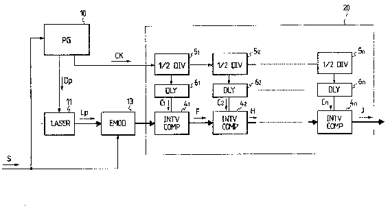
Fig. 5 illustrates in block form an embodiment
of the ultrashort optical pulse modulating equipment
according to the present invention. As shown in Fig. ~,
the ultrashort optical pulse modulating equipment of this
embodiment i5 made up of a pulse generator 10 which
regenerates clock pulses CK from an input electrical
signal S of a period T and generates electrical drive
pulses Dp each in synchronism with the clock pulses CX, a
laser 11 which is driven by the drive pulse train Dp to
generate an optical pulse train Lp, an external modulator
13 which is supplied with the optical pulse train Lp and
modulates the optical pulses in accordance with the input
electrical signal S, and an optical packet generator 20
which is supplied with the modulated optioal pulse train
and compresses the time intervals of the input optical
pulses every predetermined number of optical pulses
forming an optical packet to thereby generate compressed
optical packets each composed of a train of optical
pulses of a period ~. The external modulator 13 is
formed by, for example, an optical switch which passes
therethrough or blocks the input optical pulse, depending
-8~ V ~
on whether the level of the input electrical signal S is
high or low.
The optical packet generator 20 has an
arrangement in which the input optical pulses or optical
pulse groups are brought close to each other two by two
by each of n cascade-connected pulse interval compressors
41 through 4n~ whereby the input optical pulses are
compressed in their time intervals, for example, every m
bits forming each optical packet. The pulse interval
compressors 41 ~hrough 4n are all identical in
construction, and one of them is constructed as shown in
Fig. 6, for instance. In Fig. 6 a train of modulated
optical pulses or a train of modulated optical pulse -
groups are applied to a 1 x 2 optical switch 17. Here, -
the second-stage pulse interval compressor 42 will be
described. Assume that optical pulse groups Gl, G2, ....
each composed of two successive modulated optical pulses
of the period 1, are applied from the preceding stage
with a period of 2T as shown at row B in Fig. 7. If a
group composed of one optical pulse is also called a
group, then the following description will apply to the
pulse interval compressors 41 through 4n of all the
stages. The optical groups Gl, G2~ ... are alternately
distributed by the optical switch 17 to optical delay
lines 14l and 142 in accordance with the ON/OFF state of
a control signal C2 shown at row A in Fig. 7. The thus
distributed optical pulse groups are delayed by the
optical delay lines 141 and 142 for periods of time d
and d2, respectively. The delay times dl and d2 are
determined by adjusting the lengths of optical fibers of
the optical delay lines 14l and 142 so that the optical
pulse groups Gl and G2 are contiguous with the period I -
as depicted at rows C and D in Fig. 7. As will be seen
:., ,, , ., ,. .,, . . . .. . ,, . , , .. . , . . ~, . - , . . ,; .
2 0 ~ f3 ~3
from Fig. 7, dl = 2T -If- 21 = d2 in the second-stage pulse
interval compressor 42 and dl - 2n x T + 2n x 1 = d2 in
the nth-stage pulse interval compressor 4n. The optical
pulse groups Gl and G2 thus delayed are coupled by an
optical coupler l9, from which they are each supplied, as
a new optical pulse group composed of four modulated
optical pulses, to the next-stage pulse interval
compressor 43 with a period of 4T, wherein the interval
between every two successive pulse groups is to be
compressed to provide an optical pulse group composed of
eight modulated optical pulses. In general term, a jth-
stage (where l ~ j < n) pulse interval compressor 4j is
supplied with a train of optical pulse groups each
composed of 2i-l modulated optical pulses of the period
and brings them close to each other every two groups,
thereby creating an optical pulse group composed of 2i
modulated optical pulses.
The control signal C2 for controlling the
switching of the optical switch 17 turns ON and OFF at
intervals of 2T (i.efff with a period of 4T) in the case of
the pulse interval compressor 42 which operates as shown
in Fig. 7, and as will be seen from the above, the pulse
interval compressor 43 of the next stage is supplied with
a control signal C3 which turns ON and OFF with a period
25 Of 8T. That is, the periods of the control signals Cl to
Cn which are applied to the pulse interval compressors 4
to 4n in Fig. 5 are set to 2T, 4T, ..., 2nT,
respectively. The control signals Cl to Cn are produced
by frequency dividing the clock pulses CK of the period T
from the pulse generator l0 by cascade-connected l/2
frequency dividers 51 to 5n one after another. The
outputs of the respective stages of the l/2 frequency
dividers 5I to 5n are applied as the control signals C
, , . , !, ~ ', ' ' ;; ' ' ~ ' ' ;' ' '
20~3~
- 10-
to Cn to the pulse interval compressors 41 to 4n via
delay circuits 61 to 6nt respectively. Each of the delay
circuits 61 to 6nl or delay circuit 62, for example, is
to adjust the timing of, for example, the control signal
C2 so that it turns ON and OFF in the time interval
between adjacent optical pulse groups Gl, G2, ... shown
at row B in Fig. 7 which are provided to the optical
switch 17 of the pulse interval compressor 42.
Next, a description will be given, with
reference to Fig. 8, of the operation of the ultrashort
optical pulse modulating equipment shown in Fig. 5. In
Fig. 8, row A shows the drive pulse train Dp or the clock
- CK generated by the pulse generator 10; row B shows the
optical pulse train Lp emitted from the laser 11; row C
shows the control signal Cl for the first-stage pulse
interval compressor 41; row D shows the optical pulse
train for input into the op~ical fiber delay line 141 of
the pulse interval compressor 41; row E shows the optical
pulse train for input into the optical delay line 142 of
the pulse interval compressor 41: row F shows the output
optical pulse train F from the pulse interval oompressor
41 (i.e. the output optical pulse train from the optical
coupler 19); row G shows the control signal C2 for the
second-stage pulse iDterval compressor 42; row ~ shows - -
the output optical pulse train H from the pulse interval
compressor 42; row I shows the control signal Cn for the
nth-stage pulse interval compressor 4n: and row J shows : -
the output optical pulse train J from the pulse interval
compressor 4n.
The drive pulses Dp of the period T ~row A in
Fig. 8) are applied fro~ the pulse generator 10 to the
laser 11, which is driven by them to emit the ultrashort
optical pulse train Lp o~ the period T (row B in Fig.8).
.
01 ~ ~3~
The optical pulse train Lp is provided to the external
modulator 13, wherein it is modulated by the electrical
signal S. The following description will be given on the
assumption that electrical signals which are applied to
S the external modulator 13 are all high-level.
Accordingly, the output optical pulse train Lp (of the
period T) from the laser 11 i5 applied intact to the
optical packet generator 20. The modulated optical
pulses Lp of the period T are provided to the optical
switch 17 tsee Pig. 6) of the first-stage pulse interval
compressor 41r by which they are alternately applied one
by one to the optical fiber delay lines 141 and 142 (rows
D and E in Fig. 8) under control of the control signal C
which turns ON and OFF at intervals of T as shown at row
C in Fig. ~. The modulated optical pulses which pass
through the optical fiber delay lines 141 and 142 are
delayed for the periods of time dl and d2, respectively,
so that output optical pulses from the delay lines are
close to each other and each pair of corresponding
optical pulses has a period 1. The optical pulse trains
derived from the optical fiber delay lines 141 and 142
are coupled together by the optical coupler 19 into a
train of optical pulse groups as shown at row F in Fig.
8, and it is applied to the pulse interval compressor 4z
Z5 of the next stage.
The pulse interval compressor 42 is supplied
with the control ~ignal C2 (row G in Fig. 8) which turns
ON and OFF at intervals of 2T as referred to previously.
The optical pulse groups of the period 2T (row F in Fig.
8), each composed of two modulated optical pulses, are
alternately applied one by one via the optical switch to
the optical fiber delay lines 141 and 142 under control
of the control signal C2 ( row G in Fig. 8). The output
:,: . .. , . .: . : . :, ~ .;.. .. . . . ,: . ... . ,.. . ., . . , , ... .: , . ~ .. .... .
~ 0 ~ ~ ~ 3 ~ .
-12
optical pulse groups f rom the optical delay lines 14l and
142 are coupled together by the optical coupler 19 into a
train of optical pulse groups of a period 4T, each
composed of four modulated optical pulses of the period
as depicted at row H in Fig. 8. Similar pulse interval
compression processing is performed also in the pulse
interval compressor of the subsequent stages.
The pulse interval compressor 4n of the nth
stage (the final stage) is supplied with the control
signal Cn of the period 2n x T (row I in Fig. B), and in
the same manner as described above, the group intervals
are compressed so that the input optical pulse groups
follow one after the other in pairs. As a result of
this, each optical pulse group composed of 2n modulated
15 optical pulses of the period I as shown at row J in Fig. --
8 is provided as a compressed optical packet signal.
As described above, the ultrashort optical
pulses of the period T, modulated by the input electrical
signal S of the period T, are compressed in their
intervals to form optical packets each of which is
composed of 2n modulated optical pulses of the period 1,
and such optical pulse packets are output from the
ultrashort optical pulse modulating equipment of Fig. 5
at intervals of 2n x T. It is evident that such an
ultrashort optical pulse modulating equipment can be
applied to the optical signal multiplexer shown in Fig.
l. Incidentally, the optical switeh 17, by which input
optical pulse groups are alternately switched one by one
to the two optical delay lines 14l and 142 in each of the
pulse interval compressors 41 to 4n shown in Fig. 6, does
not cause the 3 dB loss inherent in the 1:2 optical
splitter which forms the optical splitter 12 in Fig. 3,
and consequently, the power level of the input optical
2 ~ t 5 f-~ .',' 9
-13-
pulses is held when they are alternately switched to the
optical delay lines 14l and 142. The equipment of the
present invention also employs the optical coupler l9
( Fig . 6), which causes an optical power loss of 3 dB. In
the following table I there are compared the conventional
equipment of Fig. 3 and this invention equipment of Fig.
5 in the case where the number of bits m forming each
optical packet in the former is equal to the number of
bits 2n forming the optical packet in the latter, that
is, where m = 2n.
Table I
~ Fig. 3 Fig. S
Number of Optical delay lines Optical delay lines
optical 14i to 14m 2n 14l and 142, n stages
delay lines . 2n
Number of 2n l
external
modulators
_ _
Number of 1:2 optical Switches: n, 2:1
optical splitters: 2n-1, optical couplers: n
elements 2:1 optical total of 2n
couplers: 2n-l
total of 2n~l-2
_ _
Optical 6n . 3n : .
power loss (by optical (by optical
in d~ splitters and couplers) .
couplers)
_
As shown in Table I, if n > 3, the numbers of
optical delay lines, external modulators and optical
elements needed in the ultrashort optical pulse
modulating equipment of the present invention are smaller
2~1,tj~39
-14-
than in the prior art equipment; and as the value n
increases, the constitution of the present invention
becomes particularly advantageous over the prior art.
Moreover, the overall optical power loss by the optical
splitters and the optical couplers according to the
equipment of the present invention is always smaller in
the optical power loss than the conventional equipment
for n 2 l. --
Next, a brief description will be given of an
experiment conducted on the ultrashort optical pulse
modulating equipment o~ the present invention. Fig. 9
shows in'block form an experimental version of the
equipment actually constructed with n = 2 so as to
confirm its operation.
Clock pulses CK of l GHz are generated by a
synthesizer 10a in the pulse generator 10 and drive
pulses Dp are generated by a comb generator 10b on the
basis of the clock pulses CK. The drive pulses Dp are
applied to a DFB laser 11, together with a bias current
from a current source 32, causing the laser diode ll to
produce short-width optical pulses by a so-called gain
switching method of a semiconductor laser. The optical
pulses are subjected to linear pulse width compression by
a dispersion shifted fiber 33 to obtain ultrashort . :
optical pulses Lp each having a pulse width (a full width
at half maximum) of 22 ps and a repetition frequency of 1
GHz. On the other hand, the clock pulses CK from the
synthesizer 10a are applied to a signal generator 31 to
thereby generate signals S synchronized with the clock .
pulses CK. The signals S are provided to the external
modulator 13 for intensity modulating the optical pulses
Lp in accordance with the ON/OFP state (high/low level)
of the signals S. In this experiment the signals S were
2 ~ 3 .~
-15-
all high-level. The modulated optical pulses are applied
to the first-stage pulse interval compressor 41~ wherein
they are alternately switched one by one to the two
optical fiber delay lines 141 and 142 by the 1 x 2
optical switch 17. The control signals Cl and C2 to the
switches 17 are signals of 500 and 250 MHz, obtained by
sequentially frequency dividing the clock pulses CR from
the synthesizer lOa by the 1/2 frequency dividers 51 and
52. The control signals Cl and C2 are timed by adjusting
the lengths of the delay lines 61 and ~2 and are provided
to the two optical switches 17, respectively. The
optical pulses delayed by the optical fiber delay lines
141 and 142 of the pulse interval compressor 41 are
coupled together by the optical coupler 19, whereby
optical pulse groups, each composed of two closely spaced
optical pulses, are created at a repetition frequency of
500 MHz. The optical pulse groups are further provided
to the next-stage pulse interval compressor 42~ by which
optical pulse groups, each composed of four closely
spaced optical pulses, are produced at a repetition
frequency of 250 MHz. The optical pulse trains thus
obtained were detected by a streak camera 34 and observed
on a television monitor 35, and as a result of this, it
was confirmed that optical packets (i.e. cells) of 25
Gb/s had been generated.
It is evident that the pulse interval compressor
shown in Fig. 6 may be of an arrangement in which the 1 x
2 optical switch 17 is replaced by a 1 x k optical switch
(where k i5 an integer equal to or greater than 2) so
that input optical pulses or optical pulse groups are
sequentially applied to k optical delay lines 141 to 14k.
In such an instance, a jth-stage (where 1 ~ j < n) pulse
interval compres50r 4~ is supplied with optical pulse
2~ 33
-16-
groups each composed of Mj (where M1 = 1) modulated
optical pulses of the period 1, and the optical groups
are sequentially applied to and properly delayed by the k
optical delay lines 141 to 14k and then coupled together
by the optical coupler 19, thereby producing optical
pulse groups each composed of Mj~l = k x Mj consecutive
modulated optical pulses of the period 1.
As described above, according to the present
invention, since the pulse intervals are compressed
cumulatively by applying optical pulses to n series-
connected pulse interval compressors one after another, ~-
the structure for pulse interval compression can be made
markedly smaller than the conventional structure
involving parallel processing. Hence, the ultrashort
optical pulse modulating equipment can be made small and
low-cost accordingly. Moreover, each pulse interval
compressor employs the 1 x k optical switch instead of
using an optical splitter so that optical pulses or
optical pulse groups are applied one by one to a
plurality of optical delay lines, and hence the optical
power loss throughout the equipment is small.
It will be apparent that many modifications and
variations may be effected without departing from the
scope of the novel concepts of the present invention.
., , . . . :: . : .. , - .. . . .
.: . .. . ... , . , . , . . , . ~ . ,
,, , ... , .,, ,, , .. ,.-. . . ~ . :: ;. -.. ~., . .:. : .. -