Note : Les descriptions sont présentées dans la langue officielle dans laquelle elles ont été soumises.
~t31 .~709
-1- W.E. 55,313
INTEGRATED TFEL FLAT PANEL FACE AND EDGE
EMITTER STRUCTURE PRODUCING MULTIPLE LIGHT SOURCES
CROSS REFERENCE TO REL~TED APPLICATION
Reference is hereby made to the following
copending applications dealing with related subject
matter and assigned to the assignee of the present
invention:
101. U. S. Patent Application Serial No.
filed April 24, 1989, entitled "A Multiplexed Thin Film
Electroluminescent Edge Emitter Structure And Electronic
Drive System Therefor". (W.E. 54,925)
2. U. S. Patent Application Serial No.
15353,316, filed May 17, 1989, entitled "Thin Film
Electroluminescent Edge Emitter Structure With Optical
Lens And Multi-Color Light Emission Systems", a
continuation-in-part o~ U. S. Patent Application Serial
No. 280,909, filed December 7, 1988, which is a
continuation-in-part of U. S. Patent Application Serial
No. 248,868, filed September 23, 1988. (W.E. 55,192)
BACKGROUND OF THE INVENTION
Field of the Invention
The present invention relates generally to a
thin film electroluminescent light source, and more
2~17709
-2- W.E. 55,313
particularly, is concerned with an integrated TFEL flat
panel face and edge emitter structure for simultaneously
producing multiple light sources.
Description of the Prior Art
Electroluminescence is a phenomena which occurs
in certain materials from the passage of an electric
current through the material. The electric current
excites the electrons of the dopant in the light emitting
material to higher energy levels. Emission of radiation
thereafter occurs as the electrons emit or give up the
excitation energy and fall back to lower energy levels.
Such electrons can only have certain discrete energies.
Therefore, the excitation energy is emitted or radiated
at specific wavelengths depending on the particular
material.
Thin film electroluminescent (TFEL) devices that
employ the above-mentioned electroluminescenae phenomena
have been devised in the prior art. It is well known to
utilize a TFEL device to provide an electronically
controlled, high resolution light source. One
arrangement which utilizQs the TPEL dev$ce to provide the
light source is a flat panel display system, such as
disclosed in U. S. Patents to Asars et al (4,110,664) and
Luo et al (4,006,383), assigned to the assignee of the
present invention. In a TFEL flat panel display system,
light emissions are produced substantially normal to a
face of the device and 80 provide the light source at the
device face. Another arrangement utilizing the TFEL
device to provide the llght source is a line array, or
edge, emitter, such as dlsclosed in a U. S. Patent to Kun
et al (4,535,341), also assigned to the assignee of the
present invention. In a TFEL edge emitter system, light
emissions are produced substantially normal to an edge of
the device and so provide the light source at the device
edge. A printer is disclosed in the Kun et al patent
7 0 9
-3- W.E. 55,313
which employs a TFEL edge emitter device as the light
source.
It is known in the prior art to provide the TFEL
device either as a face emitter structure for
applications requiring a large area light source, such as
a flat panel display, or as an edge emitter structure for
applications requiring only a narrow light source, such
as a light-activated printer. However, unXnown in the
prior art is an integrated structure wh$ch provides the
TFEL device as both face and edge emitter devices
suitable for applications which heretofore have been
assumed to require separate components.
SUMMARY OF THE INVENTION
The present invention provide~ an integrated
TFEL flat panel face and edge emitter structure designed
to fill the gap left by the prior art. The integrated
TFEL flat panel structure can produce multiple light
sources for concurrent applications, such as displaying
and printing the same image.
Accordingly, the present invention is directed
to a thin film electroluminescent (TFEL) device for
producing multiple light sources. The device is
comprised by a TFEL flat panel structure ha~ing front and
rear faces and side edges extending between the faces.
The panel structure i8 composed of a face emitter portion
and an edge emitter portion. The face emitter portion is
operable for emitting light energy from one of the front
and back faces of the flat panel structure in a direction
substantially perpendicular to the plane of the flat
panel structure. ThQ edge emitter portion is operable
for emitting light energy from one of the slde edges of
the flat panel structure in a direction substantially
parallel to the plane of the flat panel structure.
More particularly, the face and edge emitter
portions preferably share a common substrate. In
~U17709
-4- W.E. 55,313
addition to the substrate, each portion includes a pair
of electrode layers, at least one and preferably a pair
of dielectric layers interposed between the electrode
layers and a layer of light generating material, such as
phosphor, interposed between the dielectric layers. The
electrode layers, dielectric layers and phosphor layer
are formed in a generally stacked laminar arrangement and
are disposed on the common layer of substrate material.
These and other features and advantages of the
present invention will become apparent to those skilled
in the art upon a reading of the following detailed
description when taken in conjunction~with th`e drawings
wherein there is shown and described illustrative
embodiments of the invention.
~5
BRIEF DESCRIPTION OF THE DRAWINGS
In the course of the following detailed
description, reference will be made to the attached
drawings in which:
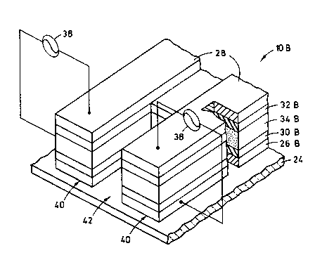
Fig. 1 iB a perspective view of an integrated
TFEL flat panel face and edge emitter structure in
accordance with the principles of the present invention,
the drive electronics for the flat panel display portion
are omitted.
Fig. 2 is an enlarged fragmentary perspective
view of an edge emitter portion of the structure as seen
along line 2--2 of Fig. 1.
Fig. 3 is an enlarged cross-sectional view of
the face emitter portion of the structure taken along
line 3--3 of Fig. 1.
pESCRIPTION OF THE PREFERRED EMBODIMENT
Referring to the drawings, and particularly to
Fig. 1, there is illustrated an integrated TFEL flat
panel face and edge emitter structure which can provide a
~17 ~J19
-5- W.E. 55,313
solid state, electronically controlled high resolution
multiple light source. The integrated emitter structure
is a TFEL flat panel 10 having front and rear faces 12,
14 and side edges 16, 1~, 20, 22 extending between the
faces 12, 14.
In accordance with the present invention, the
TFEL flat panel 10 is composed of a face emitter portion
lOA and an edge emitter portion lOB. The face emitter
portion lOA is operable for emitting light energy from
one of the faces, for example the front face 12, of the
flat panel 10 in the direction of arrow A which is
substantially perpendicular to the plane of the flat
panel 10. The edge emitter portion lOB is operable for
emitting light energy from one of the side edges, for
example the bottom edge 16, of the flat panel 10 in the
direction of arrow B which is substantially perpendicular
to arrow A and parallel to the plane of the flat panel
10. The face and edge emitter portions lOA, lOB of the
flat panel 10 can share a common substrate 24, as shown
in Fig. 1, or separate substrates placed end-to-end, as
represented by the dashed line in Fig. 1. The material
of the substrate 24 is typically glass which is
transparent to light energy.
The face and edge emitter portions lOA, lOB of
the flat panel 10 each employ a laminar stack of
substantially identical layers. As seen in Figs. 2
and 3, the respective face and edge emitter portions lOA,
lOB are each composed of a pair of electrode layers 26A,
28A and 26B, 28B, at least one and preferably a pair of
dielectric layers 30A, 32A and 30B, 32B interposed
between the electrode layers and an active layer 34A,
34B of light generating material interposed between the
dielectric layers. By way of example, the dielectric
layers 30A, 32A and 30B, 32B are composed of a high
dielectric strength, high dielectric constant material,
preferably yttrium oxide (Y203). The layer 34A, 34B of
light generating material is preferably zinc sulfide
- 2017709
-6- W.E. 55,313
doped with manganese (ZnS:Mn). Preferably, the control
electrodes 28A, 28B of the face and edge emitter portions
lOA, lOB are separate from one another permitting
selective excitation for creating images in the light
emitted by the layers 34A, 34B. The same or different
images can be created. An electrical connector 35 is
shown in Fig. 1 connected to the control electrodes 28B
of the sdge emitter portion lOB. The control electrodes
28A of the face emitter portion lOA are shown in the form
of a matrix in Fig. 1.
The layers 26A, 28A, 30A, 32A of the face
emitter portion lOB can be integral with the layers 26B,
28B, 30B, 32B of the edge emitter portion loB of the
flat panel 10. Alternatively, the respective stacks of
layers of the face and edge emitter portions lOA, lOB can
be optically separated or isolated from one another to
avoid cross talk and noise between them. However, the
separated stacks can still be disposed on a common layer
24 of substrate material.
In operation, an alternating current source 36,
38 coupled across the electrode layers 26A, 28A and 26B,
28B is operated to energize the respective face and edge
emitter portions lOA, lOB. The active layer 34A, 34B
will lum~nesce and light emitted therefrom will be
externally transmitted through the front face 12 and
bottom edge 16, respectively. The light transmits
through the front face 12 of the face emitter portion
lOA of the flat panel lO in view that the electrode layer
28A at the back face 14 is opaque or non-transparent to
light energy, whereas the electrode layer 26A at the
front face 12 next to the substrate 24 is transparent to
light energy. Also, all side edges 18, 20, 22 of the
flat panel 10, except the bottom side edge 16 of the edge
emltter portion lOB, are opaque to light energy. On the
other hand, the light transmits through the bottom edge
16 of the edge emitter portion lOB of the flat panel 10
in view that both electrode layers 26B, 28B are opaque or
%0~7709
-7- W.E. 55,313
non-transparent to light energy. By way of example, the
transparent electrode can be composed of indium-tin oxide
(In,Sn)02, and the opaque electrodes can be composed of
aluminum ~Al).
As is well known, the edge emitter portion lOB
can be provided as a multiplicity of pixels 40 separated
by a generally rectangular channel 42 formed in the TFEL
flat panel bottom edge 16. The channel 42 typically
extends vertically through the layers 26, 28, 30, 32 to
the substrate 24 and also a preselected distance
rearwardly from the edge 16 into the central portion of
the TFEL edge emitter portion lOB. The channels 42 serve
to optically isolate adjacent pixels from one another to
prevent optical cross-talk. The front edges of the
pixels 40 of the TFEL edge emitter portion lOB are the
light emission sources thereof. Typically, the rear
edges (not shown) of the pixels 40 are coated with a
layer of non-metallic reflective coating.
Potential applications for the integrated TFEL
flat panel face and edge emitter structure are those
where concurrent light images are desired, for example, a
display provided by the face emitter portion lOA for
generating a visual picture and a printhead provided by
the edge emitter portion lOB for generating a hard copy.
It is thought that the present invention and
many of its attendant advantages will be understood from
the foregoing description and it will be apparent that
various changes may be made in the form, construction and
arrangement of the parts of the invention described
herein without departing from the spirit and scope of the
invention or sacrificing all of its material advantages,
the forms hereinbefore described being merely preferred
or exemplary embodiments thereof.