Note : Les descriptions sont présentées dans la langue officielle dans laquelle elles ont été soumises.
`` 20~792S
ELECTRONIC SYSTEMS AND EFFECTIVE REDUCTION OF ELECTROMAGNETIC
INTERFERENCE ENERGY PROPAGATION FROM ELECTRONIC SYSTEMS
Introduction
The invention is in the field of electronic systems
which rely upon clock signal pulses to regulate their pace of
operation. More particularly the invention relates to
effectively reducing the propagation of electromagnetic
interference normally associated with the operation of
electronic systems.
;
Backaround of the In~ention
Electronic systems, for example systems ranging
from small personal computers to large central office
telephone exchanges, characteristically generate and radiate
electromagnetic interference. One of the sources of radiated
electromagnetic interference is that portion of an electronic
system which is characterized by a multitude of logic gates
and bistable elements, often referred to as digital
,J~ circuitry. During operation, the digital circuitry depends
upon at least one source of clock signal pulses for an
orderly timing of switching occurrences in the logic gates
and bistable elements. An electromagnetic energy pulse
accompanies each switching occurrence and propagates
outwardly, away from the electronic system, directly through
the air or space and also via àny communications leads or
power leads connected to the system. The effects of this
energy upon other nearby electrical and electronic systems
may vary greatly, however such effects are always
deleterious. In extreme cases, electromagnetic interference
has rendered an electronic system inoperative and in some
rare instances an apparatus has been known to suffer
; sufficiently to be rendered inoperative even after the
interference has been removed.
In view of the extremely serious consequences which
may accompany electromagnetic interference, manufacturers
have been forced, as a matter of practicality and at
significant expense, to provide protection such as shielding
- .
~ Z017925
~; 2
' of cabinets and cable runs, and filters for power and
~: communications leads. The effect of this protection is to
- reduce both entry and egress of electromagnetic energy. Oneexample of a cabinet design incorporating shielding is
disclosed in United States Patent No. 4,679,867 issued
14 July 1987 to S. Heldenbrand et al and titled "Cabinet for
an Electronic Apparatus". Futhermore, in various countries
national regulatory agencies have promulgated standards as to
limits of permissable levels of electromagnetic radiation.
Before an electronic apparatus may be sold or used, a
supplier of the apparatus must have been able to demonstrate,
to the satisfaction of the regulatory agency, that in normal
operating circumstances the electronic apparatus does not
; radiate unwanted energy in designated frequency ranges in
excess of the permissable levels. With the ever increasing
densities of such electronic systems being brought into use
in cities and towns, some of the regulatory agencies have
been moved in recent years to further reduce the permissable
levels of unwanted electromagnetic radiation, with the intent
of stemming what might otherwise become a torrent of
electromagnetic radiation pollution.
As is well known to persons of typical skill in the
technology of digital circuit apparatus and systems, the
generation of electromagnetic interference is a direct result
of the clock synchronous manner in which these systems
operate. Although a change of the aonduative state of any
one switch element is accompanied by only a minuscule amount
of electromagnetic interference generation, millions of such
devices all switching in step synchronism one with the other
typically generate a substantial amount of potentially
troublesome radiation. Recently larger digital apparatus
such as main frame computers and telephone switching systems
of old design and current manufacture have had to be
redesigned or modified with retrofits in order to meet the
more stringent requirements.
.
:
- Z01~9ZS
Summary of the Invention
It is an object of the invention to modify
electromagnetic interference typically radiated during
operation of digital electronic equipment by dispersing
concentrations of such radiation.
It is also an object of the invention to reduce the
effects of electromagnetic interference radiations which
normally emanate during operations of digital electronic
equipment, for example an electronic telephone system.
The invention includes a method for operating a
: plurality of logic gates for performing a function in an
electronic system. The method comprises the steps of
generating clock signal pulses at a rate which is changing
; from moment to moment, and switching each logic gate of the
plurality of logic gates between electrical logic states, as
appropriate for performing said function and at times limited
by and in synchronism with occurrences of the clock signal
pulses. A rate of change is selectable whereby
electromagnetic radiation originating in the electronic
system during its operation is of lesser interference effect
than would be so if the clock signal pulses were generated at
a substantially monotonous rate.
In one example in accordance with the invention, an
electronic system includes a digital processor, having input
and output port means, and being operable in response to
energizing current and clock signal pulses of up to and
including a maximum freguency of occurrence, for executing
processor functions in synchronism with the pulse
occurrences. A clock signal source generates the clock
signal pulses at a predetermined freguency of occurrence
~i being less than said maximum frequency of occurrence, and a
dither means is connected to the clock signal source means
for causing the frequency of occurrence to be varied about
the predetermined frequency of occurrence such that an
~ 35 average of the frequency of occurrence corresponds to the
`~ predetermined frequency of occurrence. The input and output
port means corprises a synchronous receiver transnitter being
. .
,
~`
2017925
, .
operable for coupling digital signals with the digital
processor in response to clock signal pulses from a plurality
of clock signal sources including said clock signal source
means.
In another example, an advantage of the invention
can be realized in a communication system having a TDM
network operated at a predetermined rate as directed by a
digital controller which is operated at a continuously
varying rate.
In a further example, the invention resides within
an eleetronie telephone system or seleetively eoupling
telephone station sets and the like, in communieation one
with another as directed by a central processing means, which
ineludes a digital proeessor, for direeting eall progresses
between ports of a time division multiplex switching network.
? The eleetronic telephone system includes:
a cloek signal souree means for generating elock
signal pulses at a predetermined frequeney of oeeurrence
being less than a maximum frequeney of oeeurrenee;
dither means, eonneeted to the eloek signal source
means for eausing the frequeney of oeeurrenee to be varied
about the predetermined frequeney of occurrence such that an
~ average of the frequeney of oeeurrenee eorresponds to the
3 predetermined frequeney o~ oeeurrenee: and
!25 sequenee signal generating mean5 ~or generating
ehannel and frame timing signals for regulating switehing and
transmission operations of the time division multiplex
switching network, in response to the clock signal pulses,
whereby a radiated electromagnetic energy byproduct,
associated with the normal operation of the electronic
3 telephone system, is dispersed over a wider frequency
spectrum than would otherwise be so.
In yet a further example of the electronic
telephone system, one of the ports is a digital port for
'J` 35 receiving communications signals from a digital signals
communication path. In this example the electronic telephone
system further includes a synchronizing means being connected
- ,
.~ .
- 2017925
between the time division multiplex switching network and the
, digital port. The synchronizing means is responsive to the
clock signal pulses from the clock signal source, and to
timing information associated with the received communication
5 signals, for transferring information contained therein to
- the time division multiplex switching network. More
specifically the synchronizing means comprises an elastic
. memory of a predetermined memory capacity. The elastic
r memory includes: a write port for receiving the information
10 content of the received communicaCions signals from the
digital port, in synchronism with said timing information; a
read port for transmitting the information content having
been received at the write port, to the time division
multiplex switching network, in synchronism with said clock
15 signal pulses, and means for generating an overflow signal in
an event of more than a maximum fraction of the predetermined
memory capacity becoming occupied by the information content
~' from the digital port. In this example the clock signal
source means is operable for causing the frequency of
.~, 20 occurrence to be momentarily increased, in response to an
occurrence of the overflow signal, and thereby reduce the
fraction of memory capacity being occupied.
. An example of an electronic clock in accordance with
the invention includes a con~rollable oscillator and an
p 2S alternating signal source. The oscillator is operable for
generating a clock signal, the frequency of which is varied
in response to an alternating signal from the alternating
signal source. The alternating signal may be of a sawtooth
wave form, a triangular wave form or of a pink noise nature.
0 A ratio of a minimum rate of change of the frequency of the
clock signal taken over the highest fundamental frequency
,, component of the alternating signal from the alternating
signal generator is preferred to be greater than 0.05.
$ 35 Brief DescriDtion of the Drawinas
xample embodimen~s are discussed with reference to
. the accompanying drawings in which:
;
'
.
.~ .
. . .
'.
Z0179ZS
, 6
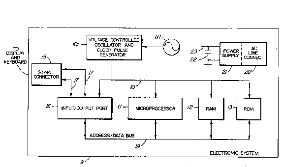
Figure 1 is a block schematic diagram of an
electronic system in accordance with the invention;
Figure 2 is a graphical representation exemplary of
spectoral frequency distribution of periodic clock signal
pulses as generated during operation of a typical digital
electronic system;
Figure 3 is a graphical representation, exemplary
of spectoral frequency distribution of dithered periodic
clock signal pulses as generated during operation in
accordance with the invention, of the eleotronic system
illustrated in figure l:
Figure 4 is a block schematic diagram of an
electronic system similar to, but more extensive than, the
~ electronic system in figure l;
!~ 15 Figure S is a block schematic diagram of an
electronic telephone system in accordance with the invention;
Figure 6 is a block schematic diagram of a timing
~ apparatus useful for providing clock pulse signals for any of
i the electronic systems illustrated in figures 1, 4 and 5; and
Figure 7 is a block schematic diagram of a timing
apparatus adapted to cooperate with a digital trunk interface
apparatus as illustrated in figure 5, whereby communications
information may be efficiently exchanged between a channel of
a time division switching network in accordance with the
invention and a digital communication signal path.
Description of the Prefe~red Embodiments
In the accompanying drawings, elements thereof are
~ labeled for convenient reference in the description. Some of
; the figures include elements which are common to several
figures, and in these cases the illustrated elements are
identified with corresponding reference labels. Furthermore,
details which are of common knowledge to those of typical
skill in digital electronics, such as supply and distribution
power and specific examples of implementation of functional
elements, are illustrated only in so far as is convenient to
exemplify the invention.
.~ .
:
20179Z5
The electronic system illustrated in figure l is
contained within a cabinet 8 and includes various logic
elements connected, via a timing lead 10, to a clock. In
this example the frequency modulated clock is provided by a
voltage controlled oscillator 101 and an alternating current
signal generator lll connected to cause a frequency of
occurrence of clock signal pulses from the voltage controlled
oscillator 101, tG be continuously varied. The cabinet 8 is
usually constructed of an electrically conductive material,
~ 10 or at least includes a conductive coatlng for the purpose of
j impeding any traversing fields or electromagnetic energy.
The various logic elements include a ~ processor 11; a random
access memory (RAM) 12; a read only memory 13; and an
input/output port 16; all interconnected by an address/data
; 15 bus 19, as shown. The input/output port 16 is provided with
access outside of the cabinet 8 via signal buses 17 and a
signal connector 18. A power supply 21 acts as a source of
energizing current which is distributed to the various logic
elements via a power lead 23. The power supply 21 is
connectable via a line connector 20 to receive power from a
source outside of the cabinet 8. For simplicity of
illustration, some details characteristic of digital
electronic systems are not shown or are shown in an
abbreviated form. For example, the power lead 23 is only
partially shown and of several capacitors 22 which are
normally distributed along the power leads of any such
system, only one is likewise illustrated.
In operation, as is well understood by persons of
typical skill in the art of digital electronic circuits, the
generation of electromagnetic interference is a direct result
of the clock synchronous manner in which these circuits
operate. Although a change of the conductive state of any
one logic element is accompanied by only a minuscule amount
of electromagnetic interference generation, such devices all
switching in step synchronism one with the other generate an
~^ accumulative electromagnetic disturbance which tends to
propagate, but which may be substantially restricted to the
.
'' , . -
,:
-- 2017925
interior of the cabinet 8. Such restriction is typically
achieved for example, by selection of appropriate material
for construction of the cabinet 8 and by providing the
connectors 18 and 20 with filters of the lowest practical
pass bands. However such restriction is not without
significant expense, which can rise in proportion to both the
size of a system, and the number of leads and the nature of
the leads which are required to be connected through the
boundary of the cabinet. It is typical practice to operate
such systems with a stable clock source of the signal pulses,
; for example to achieve a consistently optimum functional
; throughput while avoiding any abberations which might from
time to time clock a system at a rate at which it is unable
to perform satisfactorily. This practice has the effect of
generating electromagnetic radiation with energy
concentrations at the fundamental frequency of the clock
signal pulse occurrences and at several harmonics thereof, as
typified in figure 2. (Figures 2 and 3 each include a
vertical axis representative of power and a horizontal axis
; 20 representative of frequency.) On the other hand, when the
operation of the oscillator 101 is varied by the alternating
signal source, the energy concentrations may be dispersed
, somewhat as exemplified in figure 3. The dispersion of
energy is an inherent consequence of varying the frequency of
the oscillator 101, as is illu5trated or example in chapter
19 of "Transmission Systems For Communications", Third
Edition, published by Bell Telephone Laboratories,
Incorporated, in 1964. In a system operated with clock pulse
repetition frequencies in a range between 11 and 12
megahertz, with a deviation of about 250 KHz at a modulating
frequency of about 100 KHz, tests indicate that at least 6
decibels reduction of electromagnetic interferences as
compared to the same system in which the clock is of a
monotonous frequency.
In figure 4, the electronic system includes a
plurality of digital signal processors, namely a digital
processor 32 and a digital processor 36, each being connected
' ~
'.
i
2~)179ZS
. g
to an input/output port 33 and an input/output port 37
respectively. A clock pulse generator 31 is connected via a
clock lead 34 to provide clock signal pulses to the digital
processor 32 and the input/output port 33 for their
operations. Likewise another timing signals source, in this
case a dithered clock pulse generator 35, is connected to
provide timing signal pulses via a clock lead 38 for
operations of the digital processor 36 and the input/output
port 37. In one example of operation, the input/output port
33 may exchange data ~ia a communicatlons llne 42 in a
synchronous manner or in an asynchronous manner. In the
synchronous manner the rate of data transmission and
reception occurs in lock step with the frequency of the clock
signal pulses or at some submultiple thereof. This is in
contrast to the asynchronous manner wherein the rate of data
r transmission and reception is related to the clock rate only
'~ to the extent that the data transmission and reception must
occur at a rate of less than half the frequency of the clock
signal pulses and usually the rate is less than a third of
; 20 the frequency of the clock signal pulses. The input/output
~; port 33 also communicates with the input/output port 37 via a
data line 40 and a data line 41, in this example at the
,~ synchronous rate. The average frequency of the timing signal
pulses from the dithered clock pulsè generator 35 ideally
; 25 corresponds to the frequency of the clock signal pulses from
the clock pulse generator 31, however as before discussed,
; the instantaneous frequency is varied to disperse the
frequencies of unwanted electromagnetic emissions. Therefore
the input/output port 37 must perform to capture the
30 individual data bits received from the data line 41 and to
make this information available to the digital processor 36
in synchronism with the varying rate of the pulses from the
dithered clock pulse generator 35. Hereafter this or any
similarly varied pulse rate is referred to as a dithered
35 clock. In order to perform the required function, the
input/output port 37 includes a synchronizer 37s which in
turn includes an elastic memory 37e. The elastic memory 37e
20179ZS
is a well known device which is operable to receive data bits
i into a storage space, dependent upon a write clock, and to
transmit data bits from the storage space, dependent upon a
read clock. Such devices are sometimes referred to as a
FIFO, a first in first out memory, and usually are provided
with empty and full signal ports either of which becomes
asserted, in operation, when the storage space is nearing
either an empty or a full state, respectively. The write
clock in this case is provided by the synchronizer 37s which
generates same from timing information inherent in the data
from the data line 41. The read cloak is provided on the
clock lead 38. In this example a signal assertion at the
full port of the elastic memory 37e is put to advantageous
use in that the full port is connected to the dithered clock
pulse generator via a lead 39. The dithered clock pulse
generator 35 is arranged to be responsive to the signal
assertion at the full port, to momentarily accelerate the
rate of pulse generation, and so prevent data loss which
might otherwise occur in the elastic memory 37e.
The telephone system illustrated in figure 5,
` provides communications services for telephone station sets
terminals and the like at 93a-93n and 94a-94n, via a line
circuit group 91 and a line circuit group 92 respectively.
The line circuit group 91 is ¢onnected to one peripheral
¢ircuit of a peripheral circuit group 61, and the line
circuit group 92 is connected to one peripheral circuit of a
peripheral circuit group 62. A digital trunk 50 is coupled
to the telephone system by a digital trunk circuit 70 which
is connected to another peripheral circuit group 63 via a
receive lead 74 and a transmit lead 78. Each of the
peripheral circuits provides selective channel access to a
network bus 54 via a respective network circuit in a group of
network circuits 53, under the direction of a call processor
51, connected to the group of network circuits 53 by a
control bus 52. In order to provide access, each peripheral
circuit of the peripheral circuit group 61 is connected to
one of the network circuits of the group of network circuits
~.~
.
"
.:
2017925
11
53 by a TDM loop 55 which carries thirty-two bidirectional
time division multiplex channels and connection addressing
information. Similar TDM loops 56 and 58 connect the
peripheral circuit group 62 and the peripheral circuit group
5 63 to respective network circuits of the group of network
circuits 53. Timing for operation of the network bus 54, the
group of network circuits 53, the peripheral circuit groups
' 61, 62 and 63 is generated in a dithered frequency timing
source 80. The frequency modulated timing source 80
10 generates frame, channel, and bit timing signal pulses on
~ leads 81, 82 and 83 respecti~ely, to deine'a time division
3 multiplex byte interleaved operating format as exemplified in
the lower right hand portion of figure 5. The system
~ illustrated is of a general form of which there are many
i 15 different examples, one being published in United States
~, Patent No. 4,069,399 issued on 17 January 1978, to Bruce
Barrett et al and titled ~A TD~ PCM Communication System",
and another being published in United States Patent No.
4,873,682 to George Irwin et al and titled "Digital Key
3 20 Telephone System". Hence the particulars of the illustratedsystem are discussed only 90 far as the use of the dithered
frequency timing source 80 in the system is used to achieve
some frequency dispersal of the electromagnetic radiation
byproduct of system operation.
~: 25 In operation, telephone lines connecting any o the
station sets, terminals and the like are effective radiators
' of electromagnetic energy. Their effectiveness is somewhat
; proportional to the frequencies associated with the rate of
the system operation and the harmonics thereof, and with the
; 30 length of each telephone line conductor residing within the
~' cabinetry enclosing the system. In the system illustrated in
~ figure 5, this effect is materially reduced by the use of the
'~- dithered frequency timing source 80 which in this case is
arranged to generate bit timing pulse signals having an
average frequency corresponding to a bit rate of the digital
. trunk 50. This is achieved in combination with the digital
trunk circuit 70 which includes an elastic memory 72 and an
~`
:,.
7, ,~
... .
~ . .
...
.
:
.:
2017925
12
- elastic memory 76. The elastic memory 72 functions to
. transfer information bits from the regular signal format of
;~ the receive path 73 of the digital trunk 50 to the somewhat
irregular signal format of the receive lead 74, while the
elastic memory 76 functions to perform the reverse function
between the transmit lead 78 and the transmit path 77 of the
digital trunk 50. The synchronizer 71 generates clock pulses
_~_ at the operating rate of the digital trunk 50. These are
supplied at a write input (wck) of the elastic memory 72, and
at a read input (rck) of the elastic memory 76, such that
writing and reading of the memories 72 and 76 are achieved
5, respectively with reference to the operating rate of the
digital trunk 50. Likewise bit timing pulses provided by the
dithered frequency timing source 80 on the timing bus 85 are
applied at read (rck) and write (wck) inputs of the
respective elastic memories 72 and 76 to synchronize reading
from the elastic memory 72 and writing into the elastic
memory 76 with the operating signal format of the telephone
system. The frequency modulated timing source 80 is urged to
follow on average the operational rate of the digital trunk
50 in response to assertions of full and empty signals on
full and empty leads 79 and 75, in a manner similar to that
discussed in relation to figure 4. Of course if no
reference, such as from the digital trunk 50 is available,
the frequency modulated timing source 80 may freerun or
operate with reference to some other internal clock source
such as that which is normally contained within the call
processor 51.
The timing apparatus in figure 6 is one example of
, 30 that which may be used to provide a dithered or dispersed
:~ frequency clock. In this figure, a voltage controlled
`5 oscillator 101 includes an output for supplying signal pulses
~ii to a divider circuit 103 and a sequencer 108. The sequencer
utilizes the signal pulses to generate bit channel and frame
.j 35 synchronizing signals useful for operation of any associated
communications system. The divider circuit 103 provides a
scaled signal to an EXCLUSIVE OR circuit 102. The EXCLUSIVE
. .
. .
~ ' .
. , .
'
. .
. .
"
,
2~)179ZS
. .
13
OR circuit 102 may compare the scaled signal with a signal
from a frequency reference source 106, if such is provided.
In any case the output of the EXCLUSIVB OR circuit 102
' alternates between binary states. In this example it is
convenient that these binary states correspond to positive
and negative potentials equally displaced from ground. The
output of the EXCLUSIVE OR circuit 102 is connected to a
summing point 117 of a summing integrator 115, by a resistor
104. An output of an alternating signal source 111 is
liXewise connected to the summing point 117. The summing
integrator 115 is provided by an operational amplifier 116
sometimes referred to as a differential amplifier, and which
includes an inverting input being connected by a resistor 119
to ground, a non-inverting input being connected to the
, 15 summing point 117, an output being connected to an input of
the voltage controlled oscillator 101, and a capacitor being
connected between said output and the summing point 117. In
operation at equilibrium, that is when the average frequency
of the output of the voltage controlled oscillator 101 is the
same as the signal from the frequency reference source 106 or
when there is no such signal provided, the output signal from
the EXCLUSIVE OR circuit 102 is a 50% duty cycle signal.
Hence the only variatlons of slgnificanae which will cause
the output signal to be dithered about the average operating
frequency are those of a much lower frequency than the pulse
signals from the EXCLUSIVE OR circuit 102. The alternating
signal source 111 is arranged to provide such signals. In
one example, about 100 KHz, has been found to be effective.
However other wave shapes can be used, and in particular a
;~ 30 pink noise generator also has been found to be effective when
used as the alternating signal source 111.
` In figure 7 the clock source includes the summing
integrator 115, the output of which is connected to the input
I of the voltage controlled oscillator 101 by a resistor 129.
In this case the alternating signal source 111 is likewise
connected to the voltage controlled oscillator 101 by the
resistor 112. The inputs of the summing integrator 115 are
.
:'.
Z!)17925
14
. connected by leads 132 and 142, to receive differentiations
130p and 140p of leading edges of the full and empty signals
79p and 75p as are available on the leads 79 and 75 which
originate in the digital trunk circuit 70 in figure 5. In
this arrangement the circuitry of figure 7 provides the
dithered frequency timing source 80 in figure 5 such that the
:, frequencies of the timing signals on the timing bus 85 are
dithered about, while from time to time as needs be, said
~requencies are ad~usted to be greater or lQsser and thus on
average traok with the oper~ting rate of another telephone
system trunk connocted therowith.
.,
>
.