Note : Les descriptions sont présentées dans la langue officielle dans laquelle elles ont été soumises.
1
AN INPUT CIRCUIT FOR AN ELECTRICAL ENERGY METER
The present invention relates to an input circuit for a
meter unit suitable for measuring electrical energy associated
with voltage and current signals, i~he input circuit comprising
a voltage sensor receiving the voltage signal, a current sensor
receiving the current signal, and respective voltage and
current paths for connecting said sensors to respective inputs
of the meter unit, the current sensor being in -the form of a
mutual inductance transformer and -the current path including a
phase shifting active filter based on an amplifier having -two
inputs and one output, said amplifier being associated firstly
with an AC gain adjusting resistance which is connected
upstream from the first input of said amplifier, and secondly
with a feedback connection including a feedback capacitance,
-thereby looping the output of the amplifier back onto the first
input thereof.
The term "gain adjusting resistance" is used in the
present description to designate any resistance vahich, when
changed, causes the gain to be changed, and not necessarily a
particular resistor which is actually changed in order to
adjust gain.
BACFCGROUND OF THE INVENTION
Such an input circuit is described, for example, in U.S.
patent No. 3 226 641, granted in 1965.
As is known to the person skilled in the art, and as
recalled in that prior patent, the use of a mutual inductance
as a current sensor for an electrical energy meter suffers from
a particular problem in that the signal available at the
secondary winding of such a transformer is not an image of the
signal applied to its primary, but is an image of the
derivative of said signal, as a function of time.
One known way of mitigating this difficulty is to
interpose a phase shifting active filter on the current path,
with such a filter, as taught by the above-mentioned patent,
being constituted by an integrator.
However, this solution in turn poses a new problem, which
is made particularly severe nowadays by the considerable
2
increase in -the accuracy required of electronic type electrical
energy meters, namely -that the integrator is itself liable to
generate a parasitic DC signal which may spoil -the measurement
performed by the meter circuit.
More generally, the unavoidable physical defects of -the
components used in the input circuit, in particular in the
mutual inductance transformer and in the active filter, have
the overall effect of the signal delivered by the active filter
not necessarily constituting a true image of -the current to be
measured, in particular when the active filter is a conven
tional integrator, and thus subject to a voltage offset.
In this context, a first object of the invention is to .
provide an input circuit for an electrical energy meter where
the transfer function is such that the input circuit has no
parasitic effect on the signal to be measured.
SUDM~ARY OF THE INVENTION
To this end, in the circuit of the invention, the phase
shifting active filter further includes a coupling capacitance
connected to the output of the amplifier upstream from the
feedback connection, in addition to the AC gain adjusting
resistance and the feedback capacitance,
Preferably, the active filter also includes a DC gain-
limiting resistance directly connecting the output of the
amplifier to the first input thereof.
In which case, the active filter may additionally include
an output filter comprising a passive RC filter of the
integrator typa connected upstream from the two inputs to -the
amplifier, thereby compensating for a difference between the
phase shift imparted by the active filter and a predetermined
value desired for said phase shift.
In order to make the active filter even more insensitive
to the load connected to its output, a voltage divider may be
connected to the output of the active filter upstream from said
load.
In the circuit of the invention, there is no need for the
voltage sensor to be particularly elaborate, and on the
contrary, it may be constituted merely by a voltage divider
~ ?C
~~~~~1~di.W
3
having an output connected to a junction terminal between the
first impedance receiving the voltage signal and a second
impedance connected to a reference voltage.
Fox a final correction of phase error in the active
filter, and when the circuit is applied to an active energy
meter, the first impedance of said voltage divider may
nevertheless comprise a capacitance.
In an application of the circuit to a reactive electrical
energy meter, the active filter may comprise a leakage
resistance connected in parallel with the feedback capacitance,
said filter then operating with a phase shift of 45°.
In the reactive case, it is also possible to provide for . -
the voltage path to include a second passive RC filter of the
integrator type, likewise operating at a phase shift of 45°.
A resistance is then preferably connected in parallel with
the capacitance of the second passive RC filter.
BRIEF DESCRIPTION OF THE DRAWINGS
Embodiments of the invention are described by way of
example with reference to the accompanying drawings, in which:
Figure 1 is an electrical circuit diagram of one possible
embodiment of an input circuit in accordance with the invention
for use with an active energy meter;
Figure 2 is an electrical circuit diagram of one possible
embodiment of an input circuit in accordance with the invention
for use with a reactive energy meter;
Figure 3 is a graph showing the response of a portion of
the Figure 1 circuit, in terms of the relative phase of an
output signal plotted up the Y axis as a function of frequency
plotted along the X axis, for a signal applied to the input of
said circuit portion; and
Figure 4 is a graph showing the response of the same
portion of the Figure 1 circuit, in terms of the voltage of an
output signal plotted up the Y axis as a function of frequency
plotted along the X axis, for a signal applied to the input of
said circuit portion.
DETAILED DESCRIPTION
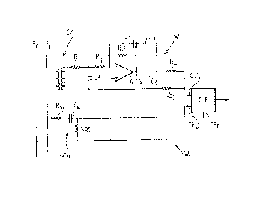
In Figure 1, FO and F1 represent two conductors of an
4
electricity distribution network, which conductors may be
connected to loads (not shown) capable of consuming a certain
quantity of energy, which energy i:~ to be measured by an
electronic meter unit CE.
The desired quantity of energy depends firstly on the
current flowing along the zonductoa~ F1 (or the conductor FO),
and secondly on the voltage that earists between the conductors
FO and Fl.
The signals associated with said current and with said
voltage are detected by a current sensor CA.i and a voltage
sensor CAu respectively which provide signals derived
therefrom, which signals are transmitted to respective inputs
CEi and CEu of the meter unit via a current path Wi and a
voltage path Wu, respectively.
In the present case, the current sensor is a mutual
inductance transformer, i.2. a ~transforrner essentially
constituted by a primary winding and a secondary winding with
direct electromagnetic coupling through air.
The current path Wi comprises a phase shifting active
filter using an amplifier A having an inverting input A-, a
non-inverting input A+, and an output S.
The amplifier is associated firstly with an AC gain
adjusting resistance R1 connected upstream from the inverting
input A-, and secondly with a feedback connection LR having a
feedback capacitance Cl interposed therein, said connection
looping the output S of the amplifier back to the inverting
input thereof.
According to an essential characteristic of the invention,
the phase shifting active filter also includes a coupling
capacitance CZ connected to the output of the amplifier
upstream from the feedback connection T~R.
The amplifier A in combination with the resistance R1 and
the feedback capacitance Cl constitutes a conventional
integrator known for applying a phase shift of 90° to any AC
signal applied to the resistance R1 together with attenuation
proportional to the frequency of the signal, which would
therefore provide a simple way of comper~sating for the opposite
;~ ; -.
5
phase shift and amplification imparted by the sensor CAi, were
it not for undesirable parasitic effects that are also
included.
In contrast, the amplifier A in combination with the
resistance R1 and capacitances C1 2md C2 ceases to behave like
a conventional integrator since the capacitance C2 impedes the
flow of low frequency currents. The relatively complex
behavior of this filter is described below.
In addition to the items already mentioned, the active
filter preferably includes a DC ga~.n limiting resistance R2
directly connecting the output S of the amplifier A to the
inverting input thereof, thereby having the beneficial effect .
of preventing the amplifier from saturating by integrating its
own offset voltage, but having the undesirable effect of
further removing 'the characteristics of the active filter A,
R1, C1, R2, C2 from the characteristics of an ideal integrator.
Under these conditions, and at least over a wide range of
frequencies, the action of this filter no longer compensates
the action on the mutual inductance transformer CAi which
itself constitutes a practically ideal differentiator, at least
fox signals in the useful frequency range.
In order to mitigate this difficulty, the active filter is
preferably provided with an integrating type passive RC filter
constituted by resistance R3 and capacitance C3 connected up-
stream from the A- and A+ inputs of the amplifier A, the
passive filter being designed to ensure that the total phase
shift of the assembly A, C1, C2, C3, R1, R2, and R3 has a value
of 90° at the outlet end thereof, which in the application
shown in Figure 1 is constituted by an active energy meter unit.
In addition to its function of correcting phase shift
error, the passive filter R3C3 has the advantage effect of
damping high amplitude high frequency transient waves that the
current sensor may generate due to its behavior as a
differentiator.
In order to make the active filter insensitive to the
external load to which it is connected, and in order to reduce
the size and the capacitance of C2 as much as possible, it may
_ ~3~x.~3~~-
6
be advantageous to connect a voltage divider such as R4, R5 at
the output of the active filter A, R1, C1, C2, R2.
The voltage sensor may simply be constituted by a voltage
divider having an output connected to a junction terminal
between a first impedance R6C~ receiving the voltage signal and
a second impedance R7 connected to a reference voltage.
In this case, any possible re~;i.dual phase shifting error
applied by the active filter and represented by a change in
phase as a function of frequency maiy be compensated by making
the first impedance in the form of a resistance and a
capacitance connected in series, while the second impedance is
purely resistive in nature.
The reference potential common to the current path Wi and
to the voltage path Wu, and also to the meter unit CE, may be
constituted by the potential of the neutral conductor F0, for
example, having the capacitance C3, the non-inverting input A+
of the amplifier A, the resistance R5, the resistance R7, and
the reference potential input CEr of the meter unit CE all
connected thereto.
Figures 3 and 4 relate to the overall transfer function of
the combination of the current sensor CAi and of -the active
filter A, R1, C1, R2, C2, with the passive fi7-ter R3C3 being
excluded from this combination.
As shown in Figure 3, this combination behaves almost like
a polarity inverter for signals having a frequency of about
1 Hz, like a 90° phase shifter for signals having a frequency
of about 7 Hz, and like a phase shifter whose effect tends to
zero for signals having a frequency of about 50 Hz or mare.
Similarly, Figure 4 shows that signals at a frequency of
less than 2 Hz are hardly transmitted at all, signals having a
frequency of about 7 Hz give rise to resonance which amplifies
them, and signals from about 50 Hz up are restored without
change in amplitude.
The guiding principles for making a practical embodiment
of the circuit shown in Figure 1 are as follows.
The resistance R1 should be high relative to the
resistance of the secondary winding of the currant sensor CAi,
A
~~~1.~_"~>~~~~~
7
for example it should not be less than 100 'times said
resistance. One possible practical value is 78,800 ohms.
The capacitance CZ may be 10 nF, for example, while C2 may
be about 2.2 uF.
The resistance R2 should be at: a fixed large value, e.g.
4.7 megohms, while suitable values for the resistances R4 and
R5 are respectively about 3,000 ohms and 2,000 ohms.
zf R4 is given a smaller value, then C1 should have a
larger value so that the product (R4+R5).C1 remains
substantially constant.
Suitable values for the resistance R3 and the capacitance
C3 are 78,800 ohms and 1.2 nF, respectively.
Suitable values for the resistance R6, the resistance R7,
and the capacitance C4 are 392,000 ohms, 2,600 ohms to 4,000
ohms, and 68 nF, respectively.
Figure 2 shows a circuit analogous to the circuit of
Figure 1, except insofar as it is for use with a reactive
energy meter unit.
This means that in this application the relative phase
shift between the voltage and current signals provided to the
inputs CEi and CEu of the meter unit CE should differ by 90°
from the relative phase shift of the voltage and current signal
actually available on the conductors FO and F1.
Since the current sensor CAi itself imparts a phase rota-
tion of 90° to the current signal and amplifies it proportional
to its frequency, the voltage path Wu and the current path Wi
are not subjected, a riori, to any constraint other than
imparting the same phase shift (possibly zero) to the signals
that they transmit together with attenuation of the current and
voltage signals suitable for compensating the amplification
applied by the sensor CAi to the current signal, and
proportional to the frequency of the signal.
The solution of the invention consists in causing each of
the voltage and current paths to impart a respective phase
shift of 45° and a corresponding attenuation of the signal,
thereby causing its amplitude to be at least approximately
proportional to the square root of the reciprocal of the
frequency common to the voltage signal and to the current
signal, with the attenuation in the two paths thus compensating
the amplification proportional to frequency as imparted by the
current sensor CAi, with respect to the signal representative
of reactive energy as delivered by the meter unit CE.
Items which perform similar functions in Figures 1 and 2
are given identical reference numerals in both of them.
Thus, in addition to the items already described above
with respect to Figure 1, the circuit of Figure 2 shows a
leakage resistance R8 connected in parallel with the feedback
capacitance C1 and having the purpose of changing the phase
shift imparted by the active filter A, R1, C1, R2, C2, R3, C3 .
to a value of 45°.
The voltage path Wu is still essentially constituted by a
voltage divider RS, R7 suitable for substantially reducing the
voltage available between the conductors FO and F1.
In addition to these items, this path also includes a
second passive RC filter of the integrator type comprising a
series resistance R9 and a parallel capacitance C5, such that
this filter likewise imparts a phase shift of 45°.
As shown in Figure 2, a resistance R10 is preferably
connected in parallel with the capacitance C5 so as to reduce
the voltage thereacross.
As will readily be understood by the person skilled in the
art, the components R6, R7, R9, R10 and C5 could be combined by
conventional equivalent impedance calculation in order to
reduce the numk~er of components used, if necessary.
In the circuit of Figure 2, the current path Wi and the
voltage path Wu apply amplification to the current and voltage
signals respectively which is substantially proportional to the
square root of the reciprocal of the frequency common to these
signals.
The combined contribution of the voltage and current paths
therefore gives rise to attenuation in the signal
representative of energy which compensates for the
amplification imparted by the current sensor CAi regardless of
the frequency o:E the current and voltage signals, at least over
a certain range about their nominal frequencies.
~~~..~3~~~
9
In addition, insofar as -the voltage path Wu and the
current path W:i are designed to impart the same phase shift of
45°, and assuming that change's in the frequency of the current
and voltage signals do not have any significant effect on the
equality of the phase shifts imparted by the voltage and
current paths, the circuit of Figure 2, when compared with
conventional circuits, presents the advantage of compensating
both for phase errors and for amplitude errors in the current
and voltage signals available on the conductors FO and Fl,
which errors would normally appear for variations in frequency
about the common nominal values.
20
30