Sélection de la langue

Search

Sommaire du brevet 2018681 

Énoncé de désistement de responsabilité concernant l'information provenant de tiers

Une partie des informations de ce site Web a été fournie par des sources externes. Le gouvernement du Canada n'assume aucune responsabilité concernant la précision, l'actualité ou la fiabilité des informations fournies par les sources externes. Les utilisateurs qui désirent employer cette information devraient consulter directement la source des informations. Le contenu fourni par les sources externes n'est pas assujetti aux exigences sur les langues officielles, la protection des renseignements personnels et l'accessibilité.

Disponibilité de l'Abrégé et des Revendications

L'apparition de différences dans le texte et l'image des Revendications et de l'Abrégé dépend du moment auquel le document est publié. Les textes des Revendications et de l'Abrégé sont affichés :

  • lorsque la demande peut être examinée par le public;
  • lorsque le brevet est émis (délivrance).
(12) Brevet: (11) CA 2018681
(54) Titre français: METHODE POUR REDUIRE LES COURANTS DE FOULCAULT DANS UNE BANDE SUPRACONDUCTRICE ET DISPOSITIF A SUPRACONDUCTEUR
(54) Titre anglais: PROCESS FOR REDUCING EDDY CURRENTS IN A SUPERCONDUCTOR STRIP, AND A SUPERCONDUCTOR ARRANGEMENT
Statut: Réputé périmé
Données bibliographiques
(52) Classification canadienne des brevets (CCB):
  • 337/3.1
(51) Classification internationale des brevets (CIB):
  • H01B 12/00 (2006.01)
  • H01L 39/14 (2006.01)
(72) Inventeurs :
  • DERSCH, HELMUT (Suisse)
(73) Titulaires :
  • ABB SCHWEIZ AG (Suisse)
(71) Demandeurs :
(74) Agent: NORTON ROSE FULBRIGHT CANADA LLP/S.E.N.C.R.L., S.R.L.
(74) Co-agent:
(45) Délivré: 1999-01-19
(22) Date de dépôt: 1990-06-11
(41) Mise à la disponibilité du public: 1990-12-14
Requête d'examen: 1997-02-05
Licence disponible: S.O.
(25) Langue des documents déposés: Anglais

Traité de coopération en matière de brevets (PCT): Non

(30) Données de priorité de la demande:
Numéro de la demande Pays / territoire Date
2229/89-0 Suisse 1989-06-14

Abrégés

Abrégé français

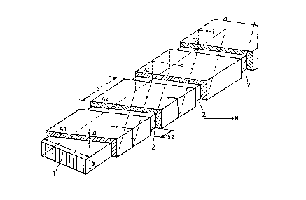
Cette invention concerne un ensemble formé d'une bande en métal non supraconducteur (1) et d'un revêtement de supraconducteurs haute température (A1, A2) électriquement anisotropes et destiné à des applications en courant alternatif telles que machines électriques et aimants où il permet de réaliser de façon relativement simple une réduction des pertes de courant alternatif dans la bande monocouche de revêtement supraconducteur haute température (A1,A2) enroulée en spirale autour de la bande en métal non supraconducteur. La bande supraconductrice (A1, A2) présente une direction privilégiée où la densité de courant critique est inférieure à celle caractérisant toutes les autres directions. Selon le montage objet de l'invention, un courant (i) circulant dans le supraconducteur (A1, A2) traverse périodiquement des régions ayant l'orientation privilégiée et des régions décalées de 180 degrés par rapport à celle-ci. Ces régions périodiques limitent la longueur des courants de Foucault. Au lieu d'un enroulement spiralé, il est également possible de réaliser, en particulier pour les câbles d'alimentation, des conducteurs à deux couches présentant, le long de la direction de circulation du courant et à intervalles appropriés, des rainures et nervures qui forcent le courant à passer périodiquement d'une couche à l'autre.


Abrégé anglais


An arrangement of electrically anisotropic
high-temperature superconductors (A1, A2) on a non-superconducting
metal strip (1) for alternating-current applications,
such as magnets and electrical machines, is
specified in the case of which a relatively simple
reduction of alternating-current losses is achieved in
that at least one strip (A1, A2), deposited as a layer,
made of a high-temperature superconductor, spirally
surrounds this metal strip. The superconducting strip
(A1, A2) has a preferred direction in which the critical
current density is smaller than in all other directions.
In this arrangement, a current (i) flowing through the
superconductor flows periodically through regions of the
superconductor (A1, A2) that are oriented in the preferred
direction and twisted by 180° thereto. These periodic
regions limit the length of the eddy currents.
Instead of a spiral winding (A1, A2), it is also
possible to use, especially for power cables, a two-layer
conductor with grooves and webs arranged periodically
along the current direction, in the case of which grooves
and webs the current must alternate periodically from one
into the other layer.

Revendications

Note : Les revendications sont présentées dans la langue officielle dans laquelle elles ont été soumises.


- 8 -
The embodiments of the invention in which an exclusive
property or privilege is claimed are defined as
follows:-

1. A process for reducing eddy currents in at least
one anisotropic current-carrying superconductor strip
(A1, A2, 3)
a) which in a preferred direction (c) has a smaller
critical current density (jl) than in all other
directions (a, b), and
b) is applied as a layer on a non-superconducting
substrate (1)
wherein
c) the eddy currents generated in the superconductor
strip are conducted segmentally at periodic intervals,
which are smaller than a predeterminable
critical length (l o), through regions of the
superconductor strip that are oriented in the preferred
direction (c) of the superconductor and oppositely
thereto (180°), it being the case that it holds for
the critical length that:
l c = 4 ((r.~.j c)/(dB/dt))1/2,
~ = electrical resistance of the superconductor in the
c-direction upon overshooting of the critical current
density in this direction, r = half strip thickness, j c =
critical current density in an a,b-direction perpendicular
to the c-direction, B = magnetic induction, and
t = time.
2. A superconductor arrangement with at least one
anisotropic superconductor strip (A1, A2, 3),
a) which has in a preferred direction (c) a smaller
critical current density (j1) than in all other
directions (a, b) and
b) is applied on a non-superconducting substrate (1) as
a layer,
c) the preferred direction (c) and the substrate
surface forming an angle of 90° ~ 5°,
wherein,
d) in the direction of a current flowing through the
superconductor strip, the superconductor strip has,
at periodic intervals (2 b1 + b2; 15) after one

- 9 -
another, current flow regions of normal current
density followed by current flow regions with a
smaller critical current density (j1), it being the
case that these intervals ~ a critical length (l c),
for which it holds that:
l c = 4 ((r ,~. j c)/(dB/dt))1/2,
~ = electrical resistance of the superconductor in the
c-direction upon overshooting of the critical current
density in this direction, r = half strip thickness, j c =
critical current density in an a,b-direction, perpendicular
to the c-direction, B = magnetic induction, and
t = time.
3. The superconductor arrangement as claimed in
claim 2, wherein
a) at least one superconductor strip (A1, A2) surrounds
the substrate (1) spirally, and
b) the substrate (1) is constructed in an essentially
rectangular fashion in cross-section, its width (x)
being larger than its thickness (y).
4. The superconductor arrangement as claimed in
claim 3, wherein
a) the substrate (1) has a width (x) in the region of
1 cm - 5 cm, and
b) a thickness (y) in the region of 0.1 mm - 2 mm.
5. The superconductor arrangement as claimed in
claim 3, wherein
a) the substrate (1) has a width (x) in the region of
2 cm - 3 cm, and
b) a thickness (y) in the region of 0.4 mm - 0.6 mm.
6. The superconductor arrangement as claimed in
claim 3 or 4 or 5, wherein neighboring windings of the
at least one superconductor strip (A1, A2) have a mutual
predeterminable strip interval (b2) in the region of
0.1 mm - 1 mm.
7. The superconductor arrangement as claimed in
claim 2, wherein
a) the superconducting layer (3) has non-superconducting
separation zones, grooves or webs (5) periodically
offset at a predeterminable interval (15) in

- 10 -
the longitudinal direction (D), which project from
the supporting side of the superconducting layer (3)
into this superconducting layer, and
b) said layer (3) has separation zones, grooves or webs
(4), which are periodically non-superconducting at
this predeterminable interval (15) and extend from
the surface of the superconducting layer (3) into
this layer.
8. The superconductor arrangement as claimed in
claim 7, wherein
a) the non-superconducting separation zones, grooves or
webs (4, 5) extend alternately perpendicularly to
the longitudinal direction (D) of the
superconducting layer (3) up to the middle of this layer
in each case, and
b) separation zones, longitudinal grooves or longitudinal
webs (6, 7) which are non-superconducting
over a segment (15) of predeterminable length,
extend in the middle in the longitudinal direction
(D) of the layer (3)
c) in the entire thickness (d3) of the superconducting
layer (3).
9. The superconductor arrangement as claimed in one
of claims 7 to 9, wherein
a) the superconducting layer (3) has a width (b3) in
the region of 2 cm - 3 cm and
b) a thickness (d3) in the region of 0.01 mm - 1 mm,
c) particularly of 0.1 mm - 0.4 mm, and
d) the non-superconducting separation zone, groove or
web (4 - 7) has a width of ~ 0.5 mm.
10. Superconductor arrangement as claimed in one of
claims 7 to 9, wherein the non-superconducting
separation zones, grooves or webs (4) which project
from the surface of the superconducting layer (3)
into the latter, and the non-superconducting separation
zones, grooves or webs (5) which project from
the underside of the supporting surface of the
superconducting layer (3) into the latter are
constructed in each case in the form of seats or

- 11 -
steps in such a way that together they have the form
of an H, the crossbar of the H being formed by the
non-superconducting separation zones, longitudinal
grooves or longitudinal webs (6, 7) extending in the
longitudinal direction (D) of the superconducting
layer (3).

Description

Note : Les descriptions sont présentées dans la langue officielle dans laquelle elles ont été soumises.


Z018~;81
TITLE OF THE INVENTION

Process for reducing eddy currents in a superconductor
~ strip, and a superconductor arrangement

CKGRoUND OF THE INVENTION

Field of the invention
The invention proceeds from a process for reduc-
ing eddy currents in a superconductor strip according to
the preamble of patent claim 1, and from a superconductor
arrangement according to the preamble of patent claim 2.

Discussion of background
In the respective preamble, the invention relates
to a prior art as it is known from DE-C2-2,654,924. In
order to overcome the disadvantage of brittleness with
respect to mechanical stresses, a strip-like conductor or
compound wire, around which a superconducting layer of
Nb3Sn round a strip of Nb i8 arranged, has been proposed.
A stabilizing layer of copper or of a copper alloy is
arranged around the superco~ucting layer, a layer,
usually soldered, being arranged between the super-
conducting layer and the stabilizing layer. An outermostinsulating layer is arranged around the stabi]izing
layer. It is given as disadvantageous that the strip has
an instability in the form of a flux ~ump due to a non-
uniform magnetic field, which i8 cA~#ed by geometrical
anisotropy and leads to problems in the development of a
magnet. Furthermore, it is known to wind individual
compound cables around a rectangular or round tube of a
stabilizing and/or a reinforcing material. In order, in
the case of alternating current applications, to avoid
disadvantageous effects due to a coupl~ng current, the
superconducting cores or strands are twisted together. A
coupling current can also be reduced by providing a
different con~ctivity for the respective cores. Further-
more, an increased contact resistance bet ~ the rele-
vant core~ can avoid a loop of the coupling current in aneffective way. In order to avoid eddy-current losses, it


. ;
.~ . . . ,, ~ .

, , . . ~ ~ .. .
. ~ . ~ . .. . , . . :
, . : .. . . : . ~

- 2nl8~81
-- 2 --
is provided that a stabilizing metal, such as copper, is
used in an insulated and mutually separated state,
instead of in a continuous, solid form. It can also be
provided that the copper is subdivided by a material of
5 high electrical resistance into individual sections.
The disadvantage of this is the relatively
expensive production of compound cables.
Concerning the relevant state of the art, refer-
ence may further be made to a publication by T. R. Dinger
et al., Direct Observation of Electronic Anisotropy in
Single-Crystal ylRA~Cu3Q7-~ in the Americal journal:
Physical Review Letters, Vol. 58, Nr. 25, 22.6.1987,
pages 2687 - 2690. There i8 a description in that refer-
ence of the electrical behavior of anisotropic high-
temperature oxide superconductors, which have a smallercritical current density in a specific direction than in
all other directions.
Production of orientated films of high-tempera-
ture superconductors is known from a publication by S.Jin
et al., High critical currents in Y-Ba-Cu-O superconduct-
ors, in the American ~ournal: Appl. Phys. Lett. 52. ~24),
13.6.1988, pages 2074 to 2076.

SUMMARY OF THE lNV~r.~lON
Accordingly, one ob~ect of this invention, as
defLned in patent claims 1 and 2, is to achleve the
ob~ect of specifying a process and a sup6Lconductor
arrangement of the type ment1oned at the beginnin~ which
guarantees in a simpler fashion a reduction of alternat-
ing-current losses in the case of high-temperature
RupeLcor.ductors.
An advantage of the invention consists in that in
the case of co~uctors for applications in externally
predetermined magnetic fields (transformer, generator,
-ch i n9 etc.), the eddy currents are limited to a short
length of the conductor. This i8 achieved by periodic
twisting of the crystal planes. There is no need for
compound supeLconductors, which are exren~ive to produce,
with thin supeLconducting filr -nts, which must be


... . . . . . ..
.

,~

: . ,
..
. .

2n~s~sl
-- 3 --
embedded in a metal matrix and twisted, in order to avoid
coupling losses between the filaments.
The electrical anisotropy of high-temperature
superconductors, which up to now has been re~arded as an
obstacle to their technical application, is exploited
here.
BRIEF DESCRIPTION OF THE DRAWINGS
A more complete appreciation of the invention and
many of the attendant advantages thereof will be readily
obtained as the same becomes better understood by refer-
ence to the following detailed description when consider-
ed in connection with the accompanying drawings, wherein:
Fig.l shows a schematic representation of a section of
a metal carrier, which is coated spirally with
two strips made of an electrically anisotropic
high-temperature superconductor;
Fig. 2 shows a representation of the eddy currents in an
electrically anisotropic high-temperature super-
conductor and
Fig. 3 shows a two-Iayer conductor made of an electri-
cally anisotropic high-temperature superconduc-
tor, which i9 applied to a metal strip, and as
has rib~ or grooves at periodic intervals for de-
limitation of eddy currents.

DESCRIP~ION OF THE PREFERRED EMBODIMENTS
Referring now to the drawlngs, wherein like
reference numerals de~ignate identical or correspon~i n~
parts throughout the several views, in Figure 1 a cuboid
carrier or substrate (1), represented in principle by a
section and made of metal plate, has a width, (x) in the
region of 0.2 cm - 10 cm, preferably in the region of
2 cm - 3 cm, and a thickne~s (y) in the region of
0.05 mm - 2 mm, preferably in the region of 0.4 mm -
0.6 mm. This carrier (1) is coated spirally with two
bifilar strips (Al) and (A2) made of an electrically
anisotropic high-temperature oxide superconductor, such
as, e.g., YBa2Cu3O7~. The layer thickness (d) of these
strips (Al, A2) is smaller than their width (bl). Located


.~

: .
~ ;,
. ",. - ~

- ,

8t~81
-- 4 --
between neighboring strips (Al ) and (A2) is an interval
or a groove (2) of a width (b2) in the region of 0.1 mm -
1 mm. Consequently, a current denoted by (i) is forced
- to circle the carrier (1) spirally, to be precise upwards
and to the right in the strip (Al) and in the opposite
direction downwards to the left in the strip (A2) in the
representation in accordance with Fig. l. By coating this
structure with two identical strips, through which the
current ~i) flows in the opposite direction, it is
possible to avoid undesired inductances.
The coating with the superconductor is done in
such a way that the crystallographic c-axis of the
material everywhere forms an angle of 90~ ~ 5- with the
surface of the substrate (1). A suitable process is
described in the publication by S. Jin et al. mentioned
at the beg;nning.
Fig. 2 shows, diagrammatically, an electrically
anisotropic high-t~ _- ature s~peLconductor having a
preferred direction (e), in whieh and in the opposite
direetion to whieh the eritical eurrent density (~1) is
smaller than in all other direetions (a, b). Arrows
indieate an eddy eurrent (iw), whieh flows in a plane
perpendicular to the direetion of a magnetie field (H)
in the supelconductor. A smaller conductivity in the
direction of the critical eurrent density (~1) limits the
strength of the eddy currents.
In the esse of applieation, the supe co~ etor
arrAng --t in aeeordance with Fig. 1 is positioned with
respeet to the magnetie field (H) in sueh a way that the
narrow side faees of the earrier (1) are located in a
vertical position of 90- + 5- to the magnetie field. In
the region of the wide faces of the carrier (1), eddy
eurrents (iw) in the supe~co~ ctor strips (Al, A2) flow
alternately through regions in this preferred direetion
(e) and perio~ic~lly throuqh regions that are oriented
oppositely thereto, i.e. are rotated by 180-. In the
region of the narrow side faees of the earrier (1), eddy
eurrents (iw) flow in the plane (a, b), so that here the
desired effeet of redueing the eddy eurrents does not


~ :, . ..
.
..


~: . . .. . .

2~18681


appear.
Fig. 3 shows another embodiment of the invention,
in which an electrically anisotropic superconducting
layer (3) or a superconducting two-layer conductor (3),
which can be perceived as composed of two layers (3.1)
and (3.2) of equal thickness, but actually consists of
one layer, is deposited on a non-superconducting carrier
(1). The superconducting layer (3) has a width (b3) in
the region of 2 cm - 3 cm and a thickness (d3) in the
region of 0.01 mm - 1 mm, preferably in the region of 0.1
mm - O.4 mm. Provided in the longitu~inAl direction (D)
of the layer (3) are, at identical or periodic intervals
(15) in the lower half layer (3.2), non-superconducting
separation zones, i.e. webs or recesses or grooves (5),
which pro~ect from the supporting surface into the layer
(3) by as much as half the thickness, and provided in the
upper half layer (3.1) there are non-superconducting
separation zones, i.e. webs or recesses or yLooves (4),
which project from the upper face of the layer (3) as far
as the center of the layer or by up to half the ~hicknpss
of the layer in the latter. Seen from the surface, webs
and grooves (4, 5) are constructed in the form of seats
or steps, with in each case a non-superconducting separa-
tion zone, i.e. a longitu~inAl web or a longitll~inAl
yLoo-ve (6) in the lower half layer (3.2), and a non-
superconducting separation zone exten~ing parallel
thereto, i.e. a longitu~inAl web or a longitu~inAl yLovve
(7) in the upper half layer (3.1) in the longitl~A;nAI
direction (D) in the middle of the layer (3). Overall,
the webs or yLvoves (4, 5) belonging to one period or one
step have the form of an H, the web drawn with dashes or
the y oove (4) extending only in the upper half of the
superconducting layer (3), and the web drawn with a
through line or the groove (5) ext0n~ing only in the
lower half of the superconducting layer (3). What has
been said above applies with reference to the c-axis. In
the crossbar of the H, the superconducting separation
zone (6, 7) reaches through the entire superconducting
layer (3). The width of the non-superconducting


~ , -: ~,, - :
!, ' " ., : ', ,
' ' "" ,, ' ', ;' , . ;' ' : '
~ ,, . ~' ' " ' .

2~i8681

separation zones, webs or grooves (4-7) is s O.S mm.
The carrier (1) is 2 cm - 3 cm wide, 0.1 mm -
2 mm thick, and over 1 km long as the case may be.
Instead of this two-strip conductor, it would
also be possible to provide a single-layer conductor (not
represented), in which the c-axis of the applied super-
conductor is twisted periodically by 180~. In this
process, the c-axis and the substrate surface form an
angle of 90~ + 5~ and 270~ + 5~, which varies between
these two values periodically with a period of width (x)
plus thickness (y) of the substrate (1).
The superconductor arrangement represented in
Fig. 3 is particularly suitable as a conductor (cable)
for current transfer, in which only the proper field
losse~ have to be reduced. Here, twisting is simulated by
a two-layer conductor, in which the current-carrying
layers are periodically interchanged. The c-axis of the
applied superconductor is oriented perpendicular to the
surface of the layer (3). The effect of the g ooves and
webs (4, 5) is that each current path alternates
periodically between the upper layer (3.1) and lower
layer (3.2). Since it is a typical feature of proper
fields of the current that they have a different, oppos-
ing direction in the plane of the upper layer (3.1) and
lower layer t3.2), eddy currents are effectively limited
to the length (15) of the periodic interval of the webs
(S) ~
It is important that eddy currents are limited to
a length in the supe,conductor which is less than a
critical length lo~ where
lc ' 4 ( (r-~ ~~o)/(dB/dt) )L/2~
a ~ electrical resistance of the supercon~ctor in the
c-direction upon overshooting of the critical current
density in this direction, r 2 half strip thickness, ~0 =
critical current density in the a,b-direction, B z
magnetic induction, and t = time for effective suppres-
sion of coupling losses. In this regard, the c-direction
of the superconducting layer (Al, A2) must be aliqned
ova~ elmingly perpen~jcular to the magnetic field (H).


, .
- , , .
~ . ': ~ . i ..

'' 2t~1868~
-- 7 --
Otherwise, eddy currents which lead to higher losses are
induced in the a-b plane. In the case of the arrangement
in the case of Fig. l, the interval must be 2 . bl + b2
- s lc. With the arrangement in accordance with Fig. 3, we
must have 15 s lc.
Obviously, numerous modifications and variations
of the present invention are possible in light of the
above teachings. It is therefore to be understood that
within the scope of the app~n~ed claims, the invention
may be practiced otherwise than as specifically described
herein.


: . : , ,. ,-, . -. . . .
,
. . : ;: . . .

. ~ ,.~ . , ,. :.;. . ~ - ,
- .

. i , . . . .
:: : . . . , - , . .

. : . . ~ :. .

Dessin représentatif
Une figure unique qui représente un dessin illustrant l'invention.
États administratifs

Pour une meilleure compréhension de l'état de la demande ou brevet qui figure sur cette page, la rubrique Mise en garde , et les descriptions de Brevet , États administratifs , Taxes périodiques et Historique des paiements devraient être consultées.

États administratifs

Titre Date
Date de délivrance prévu 1999-01-19
(22) Dépôt 1990-06-11
(41) Mise à la disponibilité du public 1990-12-14
Requête d'examen 1997-02-05
(45) Délivré 1999-01-19
Réputé périmé 2010-06-11
Correction de l'état expiré 2012-12-02

Historique d'abandonnement

Il n'y a pas d'historique d'abandonnement

Historique des paiements

Type de taxes Anniversaire Échéance Montant payé Date payée
Le dépôt d'une demande de brevet 0,00 $ 1990-06-11
Enregistrement de documents 0,00 $ 1990-11-14
Taxe de maintien en état - Demande - nouvelle loi 2 1992-06-11 100,00 $ 1992-05-22
Taxe de maintien en état - Demande - nouvelle loi 3 1993-06-11 100,00 $ 1993-05-18
Taxe de maintien en état - Demande - nouvelle loi 4 1994-06-13 100,00 $ 1994-05-31
Taxe de maintien en état - Demande - nouvelle loi 5 1995-06-12 150,00 $ 1995-05-30
Taxe de maintien en état - Demande - nouvelle loi 6 1996-06-11 150,00 $ 1996-05-24
Taxe de maintien en état - Demande - nouvelle loi 7 1997-06-11 150,00 $ 1997-05-16
Taxe de maintien en état - Demande - nouvelle loi 8 1998-06-11 150,00 $ 1998-05-19
Taxe finale 300,00 $ 1998-09-25
Taxe de maintien en état - brevet - nouvelle loi 9 1999-06-11 150,00 $ 1999-05-14
Taxe de maintien en état - brevet - nouvelle loi 10 2000-06-12 200,00 $ 2000-05-12
Taxe de maintien en état - brevet - nouvelle loi 11 2001-06-11 200,00 $ 2001-05-18
Taxe de maintien en état - brevet - nouvelle loi 12 2002-06-11 200,00 $ 2002-05-17
Taxe de maintien en état - brevet - nouvelle loi 13 2003-06-11 200,00 $ 2003-05-20
Enregistrement de documents 100,00 $ 2004-05-10
Taxe de maintien en état - brevet - nouvelle loi 14 2004-06-11 250,00 $ 2004-05-17
Taxe de maintien en état - brevet - nouvelle loi 15 2005-06-13 450,00 $ 2005-05-27
Enregistrement de documents 100,00 $ 2005-08-08
Taxe de maintien en état - brevet - nouvelle loi 16 2006-06-12 450,00 $ 2006-05-24
Taxe de maintien en état - brevet - nouvelle loi 17 2007-06-11 450,00 $ 2007-05-28
Taxe de maintien en état - brevet - nouvelle loi 18 2008-06-11 450,00 $ 2008-05-23
Titulaires au dossier

Les titulaires actuels et antérieures au dossier sont affichés en ordre alphabétique.

Titulaires actuels au dossier
ABB SCHWEIZ AG
Titulaires antérieures au dossier
ABB ASEA BROWN BOVERI LTD.
ABB SCHWEIZ AG
ABB SCHWEIZ HOLDING AG
ASEA BROWN BOVERI LTD.
DERSCH, HELMUT
Les propriétaires antérieurs qui ne figurent pas dans la liste des « Propriétaires au dossier » apparaîtront dans d'autres documents au dossier.
Documents

Pour visionner les fichiers sélectionnés, entrer le code reCAPTCHA :


Pour visualiser une image, cliquer sur un lien dans la colonne description du document. Pour télécharger l'image (les images), cliquer l'une ou plusieurs cases à cocher dans la première colonne et ensuite cliquer sur le bouton "Télécharger sélection en format PDF (archive Zip)" ou le bouton "Télécharger sélection (en un fichier PDF fusionné)".

Liste des documents de brevet publiés et non publiés sur la BDBC .

Si vous avez des difficultés à accéder au contenu, veuillez communiquer avec le Centre de services à la clientèle au 1-866-997-1936, ou envoyer un courriel au Centre de service à la clientèle de l'OPIC.


Description du
Document 
Date
(yyyy-mm-dd) 
Nombre de pages   Taille de l'image (Ko) 
Page couverture 1994-01-20 1 26
Page couverture 1999-01-07 2 79
Abrégé 1994-01-20 1 34
Dessins 1994-01-20 1 33
Revendications 1994-01-20 4 144
Description 1994-01-20 7 321
Dessins représentatifs 1999-01-07 1 10
Correspondance 1998-09-25 1 46
Cession 2004-05-10 4 328
Correspondance de la poursuite 1997-02-05 2 60
Correspondance de la poursuite 1997-02-05 2 49
Cession 2005-08-08 5 172
Taxes 1997-05-16 1 70
Taxes 1996-05-24 1 68
Taxes 1995-05-30 1 71
Taxes 1994-05-31 1 75
Taxes 1993-05-18 1 51
Taxes 1992-05-22 1 53