Note : Les descriptions sont présentées dans la langue officielle dans laquelle elles ont été soumises.
-- 1 --
Semiconductor Laser Device
This invention relates to a semiconductor laser
device capable of being used for optical fiber
communication which needs ultra high speed optical
modulation, or for optical logic circuits, and optical
connections, etc., utilized in optical computers.
The prior art will be discussed in detail
hereinbelow.
Summary of the Invention
Wher. the prior art modulation system described in
detail below is applied to a semiconductor laser having an
ordinary quantum well structure, the presence of electrons
and holes localized in the quantum well cancels the
electric field applied to the well tscreening effect),
thereby weakening the net strength of the applied electric
field. That is, ~he carrier density required for laser
oscillation is about 2 X 1018 cm 3, and, under such a
high carrier density as this, the modulation of intensity
of output power of a quantum well by application of an
electric field becomes impossible due to the screening.
It was found, as a result of the present inventors'
studies, that ~he above-mentioned modulation method
according to the prior art is usable only in a spontaneous
light radiation condition, namely, before laser
oscillation, and it is difficult to apply the method to
modulation of a semiconductor laser device.
2(~8841
The present invention contemplates a solution to
the above-mentioned technical problems involved in the
prior art.
It is accordingly an object of the present
invention to provide a novel structure of semiconductor
laser device which is capable of modulating the intensity
of output power from a quantum well by application of an
electric field, even in a laser oscillation condition.
According to one aspect of the present invention,
there is provided a semiconductor laser device comprising
an active region for radiating light, means for injecting
carriers into the active region, a resonator for
amplifying the light radiated from the active region, and
means for applying a modulated electric field to the
active region, the active region having a potential well
which comprises electrons and holes, and the active region
having a structure in which the distance between the
position of electrons and the position of holes is varied
in the potential well by the electric field applied from
the electric field applying means. In the present
invention, the position of the electrons and the position
of the holes are controlled by an electric field to vary
the spatial overlap of the wave functions which
respectively describe the electrons and the holes, so as
to control the radiation of light based on recombination
of the carriers. In the present invention, electric field
Z~188~1
-- 3 --
modulation is selected for realizing an ultra high speed
optical modulation in a laser oscillation mode. By
adoption o~ the active region in which the threshold
carrier density for laser oscillation is such a carrier
density as not to cause effective screening of a modulated
electric field, a typical value of the carrier density
being less than 1 X 1013 cm 3, it is possible to
realize an ultra high speed optical modulation caused by
an electric field.
According to one specific aspect of the present
invention, there is provided a semiconductor laser device
wherein the above-mentioned active region has a potential
well comprising a region which does not fulfill the charge
neutrality condition for free-carriers, and the optical
output power is reduced by applying an electric field in
such a direction as to enlarge the distance between the
position of electrons localized in the potential well and
the position of holes localized in the potential well. In
the present invention, electric field modulation is
selected for realizirg the ultra high speed optical
modulation in the laser oscillation mode.
The potential well comprising the region not
fulfilling the charge neutrality condition is a
representative form of structure for reducing the
threshold carrier density for laser oscillation, as
201~8841
described in detail below, which ensures an effective
action of a modulated electric field, thereby enabling
ultra high speed optical modulation in a laser oscillation
mode.
According to another specific aspect of the present
invention, there is provided a semiconductor laser device
wherein the above-mentioned region not fulfilling the
charge neutrality condition for free-carriers is formed by
selective introduction of a conductivity type impurity
into the potential well. In this case, the density of the
conductivity type impurity is desirably not less than
1 X 1013 cm 3. The introduction of an n-type
impurity, which has a greater effect on a reduction of the
threshold carrier density for laser oscillation, is
particularly suitable for the electric field modulation
used in the present invention. The impurity density is
desirably not less than 1 X 1013 cm 3 in the case of
an n-type impurity, and not less than 2 X 1013 cm 3 in
the case of a p-type impurity. An especially good effect
is obtained with an n-type impurity used in a density of
not less than 2 X 12013 cm 3 or with a p-type impurity
used in a density of not less than 5 X 1013 cm 3.
According to a further specific aspect of the
present invention, there is provided a semiconductor laser
device wherein the above-mentioned region not fulfilling
1588~1
the charse neutrality condition for free-carriers is
formed by selective introduction of a conductivity type
impurity into the vicinity of the potential well in the
active region.
According to yet another specific aspect of the
present invention, there is provided a semiconductor laser
device wherein the above-mentioned region not fulfilling
the charge neutrality condition for free-carriers is based
on a lack of symmetry of the shape of the potential well.
By appropriately devising the energy band structure of the
quantum well or the vicinity thereof, it is possible to
obtain a condition where the distance between the position
of electrons and the position of holes in the potential
well is enlarged when an applied electric field is not
present. A laser oscillation condition is obtained by
application of an electric field for modulation, in such a
direction that the overlap of the wave functions of the
electrons and holes is enlarged in the well.
According to another aspect of the present
invention, there is provided a semiconductor laser device
comprising an active region for radiating light, means for
injecting carriers into the active region, and a resonator
for obtaining laser light from the radiated light, the
active region having a potential well, the potential well
comprising a region which does not fulfill the charge
neutrality condition for free-carriers, and optical output
2018841
-- 6
power of the device being modulated by applying an
electric field to the carriers in the potential well.
Further, there is provided a semiconductor laser device
wherein the region not fulfilling the charge neutrality
condition is formed by introducing a conductivity type
impurity into the active region.
According to a further aspect of the present
invention, there is provided a semiconductor laser device
comprising an active region for radiating light, means for
injecting carriers into the active region, and a resonator
for obtaining laser light from the radiated light, a
conductivity type impurity being introduced into the
active region, whereby the optical output power of the
laser is modulated by a modulated electric field applied
to the active layer.
According to another specific aspect of the present
invention, there is provided a semiconductor laser device
wherein the conductivity type impurity is so introduced as
to cancel a screening effect of the carriers present in
the active region on the modulated electric field.
According to still another specific aspect of the
present invention, there is provided a semiconductor laser
device in which the optical output power of light
oscillated by injection of carriers is modulated by an
applied electric field, wherein the optical output power
is substantially eliminated by varying the magnitude of
20i8841
the applied electric field to enlarge the average distance
between electrons and holes to be recombined in an active
region
According to a specific aspect of the present
invention, there is provided a semiconductor laser device
wherein the optical output power is modulated by the
applied electric field while a substantially constant
driving current in the vici~ity of a threshold current for
radiation of laser light is injected.
According to yet another aspect of the present
invention, there is provided a semiconductor laser device
comprising an active region, the active region having a
potential well, the potential well comprising a region
which does not fulfill the charge neutrality condition for
free-carriers, means for injecting carriers into the
active region to cause radiation of light, a resonator for
obtaining laser light from the radiated light, and means
for applying an electric field to the active region in
order to modulate the radiation of the light.
According to a still further aspect of the
present invention, there is provided a semiconductor laser
device comprising an active region for radiating light,
8'l1
-- 8
means for injecting carriers into the active region, a
resonator for obtaining laser light from the radiated
light, and means (for instance, electrodes) for applying
an electric field for modulation to the active region,
wherein the active region has a strained super lattice
structure which is one of the structures for causing laser
oscillation with such a low carrier density as not to
cause a substantial screening of the applied electric
field. The optical output power of the device is
modulated by varying the distance between the position of
electrons and the position of holes present in the active
region by the electrodes or the like. In general, the
electric field applied to a quantum well is cancelled when
the carrier density is not less that 1013 cm 3.
Therefore, the intended object is attainable by forming an
active region (quantum well structure) capable of
oscillation with a carrier density of the order of
1017 cm 3 by use of a strained super lattice and
providing electrodes for applying an electric field for
modulation.
One advantage of the present invention is that it
is possible to realize a semiconductor laser device which
is capable of varying a quantum state by the application
of an electric field to a potential well, thereby
modulating the intensity of output power at high speed in
a laser oscillation condition.
Another advantage of the present invention is that
.
201~841
it is possible to realize a semiconductor laser device in
which the spectral chirping at the time of modulation is
extremely small. Though the limit of transmission
distance in conventional optical communication is
determined by the wavelength dispersion of an optical
fiber, the use of the present invention reduces the
influence of wavelength dispersion, thereby enabling
dispersion-free transmission.
Still another advantage of the present invention is
that it is possible to realize a semiconductor laser
device suitable for ultra high speed optical fiber
communication or for optical connection in computers.
The present invention will be described in detail
hereinbelow with the aid of the accompanying drawings, in
which:
FIG. l is a sectional view showing one embodiment
of a semiconductor laser device according to the present
invention;
FIGS. 2A and 2B are diagrams for illustrating the
fundamental principle of operation of the invention,
particularly illustrating the behaviour of electrons and
holes under no applied electric field and under an applied
electric field, respectively;
FIG. 3 is a diagram showing the relationship
between doping density and threshold carrier density;
FIGS. 4, 5A and 5B are sectional views showing
Z01~8~1
- 10 -
other embodiments of the invention;
FIGS. 6A to 6H are diagrams showing various forms
of a potential well structure provided in an active region
employed in the semiconductor laser device according to
the invention;
FIG. 7 is a schematic system showing an embodiment
of the invention in which the semiconductor laser device
according to the invention is used for optical fiber
communication;
FIG. 8 is a diagram showing an arrangement of
peripheral circuitry for a semiconductor laser device
according to the invention;
FIG. 9 is a cross-sectional view of the device
shown in FIG. 4, taken along the direction of a cavity;
FIG. 10 is a diagram showing the relationship
between the distance between the position of electrons and
the position of holes and optical output power;
FIG. 11 is a sectional view illustrating a further
embodiment of the invention;
FIG. 12 is a diagram showing the relationship
between strain and threshold carrier density; and
FIG. 13 is a sectional view of yet another
embodiment of the invention.
Hitherto, a method of modulating the intensity of
Z5 output power from a quantum well by applying an electric
field to a quantum well structure in the lamination
'~S841
direction of the structure to vary the quantum states has
been practiced, and is discussed in Oyo Butsuri [Journal
of Applied Physics (Japan)], Vol. 55, p. 210, 1986. The
principle of modulation used in the method will be
explained below while referring to FIGS. 2A and 2B.
Referring to FIG. 2A, there is shown the quantum level
(broken line) and the wave functions of electrons and
holes, when no applied electric field is present. Both
the electrons and holes are localized in the quantum well
layer, and the wave functions thereof are each symmetrical
with respect to the center of the well. When an electric
field is applied in the lamination direction of the
quantum well structure, the energy bands are inclined as
shown in FIG. 2B. Under the influence of the electric
field the symmetry of the wave functions is lost. That
is, the wave function of electrons is localized to the
left side where the energy is lower, whereas the wave
function of holes is localized to the right side, as shown
in the Figure. In other words, the position of electrons
and the position of holes differ from each other on a
spatial basis, as shown in FIG. 2B.
In this specification, the difference between the
peak position of the wave function of electrons and the
peak position of the wave function of holes is defined as
the "distance between the position of electrons and the
position of holesn, as shown in FIG. 2B. Thus, when an
Z~8841
- 12 -
electric field is applied externally in the lamination
direction of the quantum well structure as mentioned
above, the wave function of electrons and the wave
function of holes are spatially separated from each other
in the quantum well. That is, the ~distance between the
position of electrons and the position of holes" is
increased. As a result, the spatial overlap of the wave
function of electrons and the wave function of holes is
decreased, which results in a decrease in the probability
of optical transition, namely, in the oscillation
strength. In short, the intensity of output power is
varied depending of whether an electric field is present
or not. The speed of modulation, or the rate of variation
in the intensity of output power depending on the presence
or absence of an electric field, is extremely high, of the
order of picoseconds. Thus, it is possible to increase the
modulation speed by one or two orders of magnitude, as
compared with the speed attained in a direct modulation
system of a semiconductor laser according to the prior art.
A system which does not fulfill the charge
neutrality condition for free-carriers in a potential well
means a system which satisfies the following inequality:
( nO + nl ) ~ ( PO + Pl )
where nl and Pl are the densities of injected electrons
- 13 -
and holes, and nO and p0 are the densities of
electrons and holes under an uninjected condition.
However, the system not fulfilling the charge neutrality
condition, referred to in the present invention, means a
system in which the deviation of the above ine~uality from
the corresponding equality is typically not less than
1 X lol8 cm~3 that is
l(nO + nl) ~ (Po + Pl)l ' 1 X 1018 cm 3.
The present inventors have presented the idea that
an introduction of an impurity into a quantum well
structure enables a considerable lowering in the carrier
density necessary for laser oscillation, namely, the
threshold carrier density [Shin-Gaku Giho (Technical
Research Reports of the Institute of Electronics and
Communication Engineers of Japan), OQE86-63]. The concept
is realized in an electric field modulation type
semiconductor laser device. The lowering of the threshold
carrier density is based on the effect of impurity doping,
that is, the effect of reducing the stimulated absorption
term and increasing the optical gain at a given injected
carrier density. This effect is shown in FIG. 3. Because
a laser oscillation condition is obtained at a low carrier
density, an electric field externally applied to the well
for the purpose of modulation is not cancelled by the
ZO~.8841
movement of carriers locali~ed in the well. As a result,
it is possible to control the spatial overlap of the wave
function of electrons and wave function of holes. FIGS.
2A and 2B show the distributions of the electrons and
holes localized in a potential well, in the absence of any
applied electric field and in the presence of an applied
electric field, respectively. Thus, it is possible to
perform a high-speed modulation by an electric field.
The shapes of the impurity-doped portion and the
potential well may take a variety of forms, as exemplified
in FIGS. 6A to 6H. Particularly, each of the figures
shows a system in which the distribution of a conductivity
type impurity introduced into the potential well or into
the vicinity of the well is partialized to develop such a
potential field that the carriers localized in the well
are separated according to the polarity thereof. By
forming this structure, it is possible to easily separate
the electrons and holes from each other. Besides, as
shown in FIGS. 6F, 6G and 6H, it is also an effective
means for accomplishing the same purpose to maintain the
distance between the electrons and holes by providing a
step in the potential well, thereby partializing the
distribution of for example, the electrons. The
modulation in the present invention is carried out by
externally applying an electric field for modulation to
the potential well by a means for applying the
electric field. It is possible to render the laser
oscillation substantially zero, by application of a
modulated electric field. The expression ~substantially
zero~ used herein means that it is possible to eliminate
stimulated emission (all the emissions other than
spontaneous emission). The means for applying the
electric field may comprise, for instance, at least one
pair of electrodes disposed respectively on the upper and
lower sides of the potential well.
FIG. 10 shows the relationship of the distance
between the position of electrons and the position of
holes, with optical output power. The data given here was
obtained where the thickness of the quantum well layer was
10 nm. The two curves show the values obtained with
potential well structures corresponding to FIG. 6A and
FIG. 6F, respectively. In the graph corresponding to FIG.
6F, the thickness of the well layer is the total thickness
of the stepped well (two-stage well). As shown in the
Figure, the optical output power decreases with an
increase in the distance. The difference between the
structure of FIG. 6A and the structure of FIG. 6B, as seen
in FIG. 10, is based on the stepped well (two-stage well)
structure of FIG. 6F, in which electrons are liable to
drop into the lower well portion (the deepest portion) of
the steppd well, resulting in a partialized distribution
of electrons.
Z018841
Some preferred embodiments of the present invention
will now be explained while referring to the drawings.
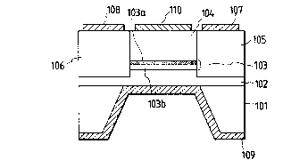
In FIG. 1, an undoped ~aAQAs clad layer 102, a GaAs
quantum well layer 103 with a thickness of 5 to 20 nm, and
an undoped GaAQAs clad layer 104 are grown on a semi-
insulating InP substrate 101. In this case, the GaAs
quantum well layer 103 is formed with two regions, namely,
an undoped GaAs layer 103b and an n-type GaAs layer 103a
doped with an n-type impurity, which is Se, Te or Si, in
an impurity density of 1 X 10¹³ to 1 X 1019 cm 3.
This structure corresponds to FIG. 6A.
In this embodiment a charge neutrality condition is
established in which the electron density in the well is
higher than the hole density in the well. Thereafter, a
projected stripe having a width of 0.5 to 5 ~m and
penetrating at least the GaAs quantum well layer 103 is
formed. Then, a p-GaAQAs buried layer 105 and an n-GaAQAs
buried layer 106 are formed, followed by formation of a
p-current injection electrode 107 and an n-current
injection electrode 108. Further, the semi-insulating
substrate 101 in the region corresponding to the projected
stripe is removed by selective etching, and electrodes 109
and 110 for applying an electric field are formed.
Finally, the system thus obtained is cleaved to obtain a
cavity length of 100 to 500 ~m.
The device produced as above on an experimental
'~188~1
basis performs laser oscillation with 2 to 15 mA. FIG. 8
shows a driving system, or a peripheral circuit, for this
embodiment. Electrodes 107, 108, 109 and 110 correspond
to those in FIG. 1, the electrode 108 being grounded. A
current injection source 841 having a function of
controlling the current injection quantity by a variable
resistor 840 is connected to the electrode 107. The
electrodes 109 and 110 for applying an electric field to
the quantum well are connected with an electric field
application source 842. When the electrode 109 for
applying the electric field was grounded and a voltage of
2V was applied to the other electrode 110 during laser
oscillation at an output of 1 to 5 mW, the laser
oscillation ceased and the optical output power was
reduced to zero. It was thus possible to modulate the
intensity of the laser output power according to the
presence of absence of an electric field applied to the
electrode 110. The switching speed in this case was about
S ps, the value being restricted by the CR time constant
of the device.
Another embodiment of the semiconductor laser
device according to the present invention is illustrated
in FIG. 4, and FIG. 9 shows a cross-sectional view of the
device, taken along the direction of a cavity. This
embodiment exemplifies an application of the semiconductor
laser device of the invention to an InGaAsP DFB laser. An
20188~1
- 18 -
undoped InP layer 402 with a thickness of 0.05 to 0.3 ~m,
an InGaAs or InGaAsP quantum well layer 403 with a
thickness of 5 to 15 nm, and an undoped InGaAsP optical
guide layer 405 with a thickness 0.05 to 0.3 ~m are grown
on an n-InP substrate 401. A grating 440 with a period of
about 240 nm is then formed on the optical guide layer
405. Thereafter, a p-InP optical confinement layer 406 is
grown. Here, the quantum well layer 403 is formed of two
regions, namely, a p-type region 403a and an undoped
region 403b. The doping density of the p-type region 403a
is about 2 X 10¹⁸ to 1 X 1019 cm 3. This structure
corresponds to FIG. 6B. A projected stripe having a width
of 0.5 to 3 ~m and penetrating the grown layers is formed,
and then a p-InP buried layer 417 and an n-InP buried
lS layer 418 are grown. A p-current in~ection electrode 407
and an n-current injection electrode 408 are then formed,
and electrodes 409 and 410 for applying electric field are
formed. Finally, the system thus obtained is cut to a
device length of 100 to 1000 ~m. The formation direction
(the direction of grooves) of the grating is orthogonal to
the stripe. In this device, the quantum well layer 403 is
sandwiched in a p/n junction, and an electric field is
therefore applied to the quantum well layer 403 due to a
built-up potential, without any voltage being applied
between the electrodes 409 and 410. Accordingly, when a
voltage of + 1 V is applied to the electrode 410, the
Z~18841
-- 19 --
energy band in the quantum well layer becomes flat.
The device produced as above on an experimental
basis performs laser oscillation with 5 to 10 mA. In this
case, the spectrum obtained indicates a single mode, which
reflects the DF8 structure. When a voltage of - 2 to - 3
V is applied to the electrode 410 for applying electric
field during laser oscillation at an opticai output power
of 5mW effected by grounding the electrode 409 and
applying + 1 V to the electrode 410, the laser oscillation
ceases and the optical output power is reduced to zero.
This switching takes place very rapidly, in 2 to 3 ps. In
addition, the spectral chirping in this case is extremely
small and is exactly the same as the chirping due to a
limit of modulation.
A further embodiment of the present invention is
illustrated in FIGS. 5A and 5B. This embodiment has a
structure resembling a two-dimensional electron gas hetero-
bipolar transistor having an emitter, a base and a
collector. A p-GaAQAs layer 502, a modulation doped
multiple quantum well active layer 503, an n-GaAQAs layer
504 and a p-GaAs layer 505 are grown on a p-GaAs substrate
501. An emitter electrode 507 is then formed.- The
modulation doped multiple quantum well active layer 503,
as is shown in detail in FIG. SB, has a periodic structure
comprising quantum well layers, each of which is composed
of an undoped GaO.9AQO.lAs layer 503bm and n doped
Z )18841
- 20 -
GaAs layer 503c, and n doped GaO.7AQo.3As barrier
layers 503a. That is, each quantum well layer is formed
of two materials differing in bandgap energy, and the GaAs
having the smaller bandgap energy is doped with an n-type
impurity. This structure corresponds to FIG. 6H.
Next, the emitter electrode 507 and the p-GaAs
layer 505 in the regions other than the above are removed,
a base electrode 508 is formed, and a collector electrode
509 is provided on the lower side. In this device, the
application of electric field to the multiple quantum well
is carried out according to the presence or absence of a
voltage applied to the collector electrode S09. Carrier
injection into the multiple quantum well is effected
through the emitter and base electrodes, and a modulation
of the intensity of laser output power similar to the
modulation in the above-mentioned embodiment is achieved.
A variety of quantum well structures are applicable
other than the forms of quantum well structures shown in
the three above described embodiments. The applicable
forms of quantum well structure are shown in EIGS. 6A to
6H, respectively. Each of the figures shows the edge of
the conduction band when an electric field is applied to
the quantum well structure. To avoid complication, one of
the quantum wells is shown in each figure. A11 these
structures are extremely effective for the respective
embodiments shown in FIGS. 1, 4, 5A and 5B.
2(~18841
FIG. 7 illustrates an embodiment in which each of
the above-mentioned semiconductor laser devices of the
present invention is applied to the field of optical
communication. A carrier injection electrode 708 and a
signal generator for applied electric field 709 are
connected to a semiconductor laser device 707. Laser
light 730 modulated by the optical device 707 is
transmitted through an optical fiber 731, and an optical
output 732 from the fiber is converted by an optical
detector 706 into an electric signal, which is
discriminated by a receiver 705. In this embodiment, it
is possible to realize a transmission speed of 100 Gbit/s
and a fiber length of 40 km.
The utilization of a strained super lattice as
another form for lowering the carrier density for laser
oscillation will be explained in detail below, while
referring to the drawings. That is, an explanation will
be given of a system in which a strained super lattice
type quantum well, or a quantum well with a lattice
constant differing from the lattice constant of an
adjacent barrier layer, is used in an active region. In
this type of semiconductor laser device, it is possible to
lower the threshold carrier density by use of a quantum
well having a particularly large lattice constant or by
use of a quantum well having a lattice constant difference
of from + 0.5 to 5%. This is because the effective mass of
Z~J.S~41
- 22 -
a hole is reduced on an equivalent basis in the strained
system, thereby increasing the optical gain and, as a
result, enabling oscillation with an injected carrier
density of about 3 to 7 X 1017 cm 3. This condition
is shown in FIG. 12. Because the laser oscillation is
realized at the low carrier density, the applied electric
field is not cancelled. It is therefore possible to
control the spatial overlap of the wave functions of
electrons and holes, and to achieve an ultra high speed
optical modulation by an electric field, as shown in FIGS.
2A and 2B. Electrodes for applying the electric field are
so formed as to enable application of the electric field
to the strained super lattice type quantum well layer.
For instance, at least one pair of electrodes may be
disposed respectively on the upper and lower sides of the
strained super lattice type quantum well layer.
This embodiment of the present invention will now
be explained referring to the drawings. In FIG. 11, a
60-A thick InGaAs strained quantum well layer 1102 having
a lattice constant greater than the lattice constant of
InP by 1.5% and a semi-insulating InP clad layer 1103 are
grown on a semi-insulating InP substrate 1101. A
projected stripe is then formed with, a 1 to 5 ~m width by
etching to such an extent as to pierce through the grown
layers. A p-InP buried layer 1104 and an n-InP buried
layer llG5 are then provided. Thereafter, a p-current
Z0188~1
injection electrode 1106, an n-current inJection ele~trode
1107 are provided, and electrodes 1108 and 1109 for
applying electric field are formed respectively on the
face side and the bottom side of the structure. Finally,
the system thus produced is cleaved to obtain a cavity
length of 100 to 500 ~m.
The semiconductor laser device produced as above on
an experimental basis performs laser oscillation with 5 to
10 mA. When the electrode 1108 for applying electric
field is grounded and a voltage of 2 V is applied to the
electrode 1109 during laser oscillation at an optical
output power of 5 mW, the laser oscillation ceases and the
optical output power is reduced to zero. Thus, it is
possible to modulate the intensity of laser output power
according to the presence or absence of an electric field
applied to the electrode 1109. The switching speed in
this case is about 5 ps, the value being restricted by the
CR time constant of the device.
Yet another embodiment of the semiconductor laser
device according to the present invention is illustrated
in FIG. 13. This embodiment has a structure resembling a
two-dimensional electron gas hetero-bipolar transistor
comprising an emitter, a base and a collector. A p-GaAQAs
layer 1302, a 100-A thick InGaA~As strained quantum well
layer 1303 having a lattice constant greater than the
lattice constant of GaAQAs by 2.5%, an n-GaAQAs layer 1304
Z()18ff41
and a ~-GaAs layer 1,05 are grown on a p-GaAs substrate
1301. An emitter electrode 1307 is provided. Next, the
emitter electrode 1307 and the p-GaAs layer 1305 in the
regions other than the above are removed, followed by the
formation of a base electrode 1308 and the formation of a
collector electrode 1309. In this device, the application
of an electric field to the strained quantum well is
carried out based on the presence or absence of a voltage
applled to the collector electrode 13Q9. Carrier
injection into the strained quantum well is effected
through the emitter and base electrodes, and a modulation
of the intensity of laser output power similar to the
modulation in the above-mentioned embodiment is achieved.
Referring again to FIG. 7, an explanation will be
given of an embodiment in which the semiconductor laser
device 707 according to the present invention, having a
strained super lattice active structure, is applied to the
field of optical communication. The semiconductor laser
device 707 shown in FIG. 11 or FIG. 13 is connected with a
carrier injection electrode 708 and a signal generator for
applied electric field 709. Laser light 730 modulated by
the optical device 707 is transmitted through an optical
fiber 731, and an optical output 732 from the fiber 731 is
converted by an optical detector 706 into an electric
signal, which is discriminated by a receiver 705. In this
embodiment, also, it is possible to realize a transmission
Z(-)18841
- 25 -
speed of 100 Gbit/s and a fiber length of 40 km.
Although the invention has been described with
reference to an ordinary double hetero semiconductor laser
device, it is to be appreciated that other semiconductor
laser devices are applicable, including a buried hetero
semiconductor laser device, a distributed Bragg reflection
semiconductor laser device, a distributed feedback
semiconductor laser device, and the like.