Note : Les descriptions sont présentées dans la langue officielle dans laquelle elles ont été soumises.
2019~66
TITLE OF THE INVENTION
Photoresists Formed bv Polymerization of Di-Unsaturated Monomers
BACKGROUND OF THE INVENTION
1. Field of the Invention
~ais invention relates to photoresists formed by polymerization of
certain substituted butadiene monomers. The invention is especially
useful in microlithography, particularly for producing semiconductor
devices on silicon chips.
2. Description of the Related Art
~ sD '~
The use of anionically or zwitterionically polymerisable monomers as
resist materials for microlithography is known in the art, as discussed ~ s~l~J/,;
in U.S. Patent No. 4,675,273 Woods et al and No. 4,675,270 Woods et al ~~
both assigned to Loctite (Ireland) Limited, the contents of which are ~r~
incorporated herein by reference. Previous methods involved spin
coating a solution of a cyanoacrylate polymer onto a substrate. U.S. ~-~t~
Patent 4,675,273 describes a method for applying a polymeric resist ,~
coating to an etchable substrate which comprises exposing the substrate ~ S~
to be coated to the vapour of an anionically polymerizable monomer of
the formula: &-r 1~ s.
',
CHR = CXY
where X and Y are strong electron withdrawing groups and R is H or,
provided that X and Y are both -CN, R may be C1-C4 alkyl, for
sufficient time to deposit a polymerizable coating thereon.
Particularly preferred monomers are 2-cyanoacrylate esters. The coated
substrate is subsequently imaged using high energy radiation; the image
is developed by conventional solvent development processes; the image
--1--
, '
2~9~66
is etched using a suitable plasma or acid etching process; and the
resist coating may be subsequently removed by heating the coating to a
temperature above the polymer depolymerization temperature.
U.S. Patent 4,675,270 describes an imaging method which comprises
(a) providing a substrate having a surface reactive to activate
polymerization of a monomer defined by the formula I as defined above;
(b) treating the surface of the substrate with a photosensitive
compound which releases an acid when exposed to actinic or ionizing
radiation; (c) subsequently imagewise exposing the substrate to
radiation of an energy effective to release said acid from said
photosensitive compound; and then (d) exposing the substrate to vapours
of one of said monomers for sufficient time to form a polymeric coating
over the substrate in the areas thereof not exposed to the radiation,
forming a relief image.
Cyanoacrylate polymers generally form positively imaged resists i.e.
I the relief image is in areas which have not been exposed to radiation
(see U.S. Patent 4,279,984 Matsuda et al, assigned to Matsushita
Electric Industrial Co. Ltd.). The process of U.S. Patent 4,675,270
also forms a positively imaged resist.
It is also known to form negatively imaged resists i.e. the relief
image is in areas which have been exposed to radiation. U.S. Patent
4,551,418 Hult et al describes a process for generating a negative tone
resist image comprising the steps of:
(1) coating a substrate with a film that contains a cationic
photoinitiator, (2) exposing the film in an imagewise fashion to
radiation and thereby generating cationic initiator in the exposed
regions of the film; (3) treating the exposed'film with a cationic-
, s,ensitive monomer to form a film of polymer resistant to plasma
etching; and (4) developing the resist image by etching with a plasma.
It is an object of the present invention to generate negatively-imaged
resists using anionic or zwitterionic polymerizable monomers.
--2--
2~196~6
l,l-disubstituted 1,3-butadienes are already known. U.S. Patent
3,316,227 Gerber assigned to Lord Corporation describes
l,l-disubstituted diunsaturated compounds having a formula selected
from the groups consisting of
/x
RlR2 \ Y 1l
and
(11)/ X
CH--C-C=C III
R2 \y
where Rl is selected from the group consisting of hydrogen, alkyl
groups containing from 1 to 5 carbon atoms, phenyl and halogen; where
R2 is selected from the group consisting of hydrogen and methyl, and
where X and Y are dissimilar electron-withdrawing groups and are
separately selected from the group consisting of cyano, carbethoxy,
ethyl sulfone, phenyl sulfone, formyl, acetyl, benzoyl, diethyl,
phosphony1, amide and phenyl. These compounds are described as having
utility in the fields of adhesives and coatings.
U.S. Patent 3,554,990 Quinn et al assigned to Eastman Kodak Company
describes esters of 2-cyanopenta-2,4-dienoic acid having the structural
formula:
/ CN
CH2=CH-CH=C \ IV
C-oR3
o
wherein R3 is an alkenyl group of 2-10 carbon atoms or an alkoxy
substituted alkyl group of 2-10 carbon atoms. These esters are said to
be useful as adhesives for general and particularly for surgical uses.
There is no suggestion in the prior art that polymers of substituted
1,3-butadienes might find utility as photoresists.
SUMMARY OF THE INVENTION
The present inventors have now surprisingly found that certain
201966~
substituted 1,3-butadienes have different and/or advantageous
propert;es, as compared to cyanoacrylates, in making photoresists.
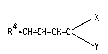
The present invention provides a polymeric resist coating comprising a
polymer o-F a monomer of the formula
R4-CH=CH-CH=C \ V
wherein X and Y are strong electron withdrawing groups and R4 is H
or, providing that X and Y are both -CN, R4 may be hydrocarbyl, aryl
or alkaryl. The term "hydrocarbyl" as used herein me~ns "aliphatic
hydrocarbyl" including alkyl, alkenyl and alkynyl. The polymeric
resist coating of the present invention has an advantage over a resist
coating of a cyanoacrylate polymer in that the coating of the present
invention has better thermal stability.
! The po1ymeric resist coating may be formed by applying a solution of
the polymer onto a substrate, for example by the known technique of
spin coating. However it is preferred to use vapour deposition.
In one aspect therefore the invention provides a method for applying a
polymeric resist coating to a substrate which comprises exposing the
substrate to the vapour of a monomer of the formula V as defined above
for sufficient time to deposit a polymeri~ed coating of the monomer on
the substrate.
In a second aspect the invention provides an imaging method comprising
applying a polymeric resist coating as defined above to a substrate,
imagewise exposing the coated substrate to high energy radiation, and
developing the image by a solvent development process to form a negative
tone image.
.
Although this invention is not limited by any theory, it is
believed that because the polymer of a dienoate monomer contains
unsaturation, the exposure to high energy radiation leads to further
crosslinking which reduces the solubility of the exposed areas as
2019666
compared to the unexposed areas. Consequently the unexposed areds are
dissolved more readily in the solvent development process. In contrast,
the polymer of a cyanoacrylate polymer is saturated and the effect of
the radiation is to degrade the polymer in the exposed areas, with the
result that these areas are more readily dissolved than the unexposed
areas.
In a third aspect the present invention provides an imaging method
comprising
(a) providing a substrate having a surface reactive to activate
polymerization of a monomer of the formula V as defined above;
(b) treating the surface of the substrate with a photosensitive
compound which releases an acid when exposed to actinic or ionizing
radiation;
(c) subsequently imagewise exposing the substrate to radiation of an
energy effective to release said acid from said photosensitive compound;
and then
(d) exposing the substrate to vapours of one of said monomers of
formula V for sufficient time to form a polymeric coating over the
substrate in the areas thereof not exposed to the radiation.
By use of the imaging method of this third aspect of the invention, a
positive tone image is produced. Thus the monomer of the formula V has
the advantage over a cyanoacrylate monomer that it can be used to
produce either a negative or a positive tone image, depending upon the
imaging method employed.
A fourth aspect of the invention comprises an imaged article prepared
. by the foregoing inventive methods.
In the definition of the monomers of formula V, the term "strong
electron withdrawing groups" refers to groups which are more electron
withdrawing than halo. Generally the electron withdrawing groups X and
Y may be independently selected from -S02R6; -S03R6; -CN;
2~19666
-CooR5 and -CoR5 wherein R5 represents a hydrocarbyl or
substituted hydrocarbyl group such as a straight chain or branched
chain C1-C12 alkyl group (which may be substituted with a
substituent such as a halogen atom or an alkoxy group), a straight chain
or branched chain C2-C12 alkenyl group, a straight chain or branched
chain C2-C12 alkynyl group, a cycloalkyl group, an aralkyl group or
an aryl group; and R6 represents H or hydrocarbyl, preferably
Cl-C12 hydrocarbyl. Preferably at least one of X and Y is -CN.
Specific examples of the groups for R5 are a methyl group, an ethyl
group, an n-propyl group, an isopropyl group, an n-butyl group, an
isobutyl group, a pent~7 group, a hexyl group, an allyl group, a
methallyl group, a crotyl group, a propargyl group, a cyclohexyl group,
a benzyl group, a phenyl group, a cresyl group, a 2-chloroethyl group, a
3-chloropropyl group, a 2-chlorobutyl group, a trifluoroethyl group, a
2-methoxyethyl group, a 3-methoxybutyl group and a 2-ethoxyethyl group.
In the monomer of formula V, R4 is preferably H but provided that X
and Y are both -CN, R4 may suitably be a Cl-C20 hydrocarbyl
group, more particularly a C1-C20 alkyl group.
The most preferred monomers of the formula V are those of the formula
/CN
CH2=CH-CH=C \ Va
CoOR7
wherein R7 is a C1-C5 alkyl or C2-C5 a1kenyl group, more
particularly ethyl 2-cyanopenta-2,4-dienoate or allyl 2-cyanopenta-
2,4-~ienoate.
In the case of deposition from solution, a polymer is prepared and thendissolved in a suitable solvent such as dichloromethane, acetone,
nitromethane, tetrahydrofuran, acetonitrile, or chloroform. In the case
of vapour deposition processes, the monomer vapours may be generated
from the monomers at ambient temperatures and pressures but it is
generally preferred to heat the monomers and/or reduce the atmospheric
pressure above the monomer generated in the chamber in order to
generate sufficient concentrations of vapour to accomplish the polymer
2019~66
deposition on the substrate in a reasonable time.
Virtual1y any substrate upon which a polymeric image is desired may be
utilized in the inventive processes. Most advantageously, the
substrates will be ones which undergo subsequent acid or plasma etching
during which the polymer coating serves as an etch resist. Suitable
substrate materials include silicon dioxide, including SiO~ coated
silicon, metallic oxides, and glass, all of which may be etched by
plasma or acid etching processes. Metallic substrates which can be
etched by acid processes, such as copper coated epoxy/glass boards used
in printed circuit board manufacture and metal printing plates may also
be utilized in the inventive process. Where the inventive process is
used to produce an etch resist, the resist coating may be removed after
etching by treatment with dilute caustic solution (e.g. NaOH) or by
exposure to a suitable plasma (e.g. oxygen plasma).
The preferred substrate is SiO2 coated silicon, e.g. the silicon
chips conventionally used in preparation of semi-conductor devices.
Most suitably, this substrate is etched by plasma etching process.
In the case of vapour deposition processes, no surface treatment will
be necessary if the substrate surface is inherently active for inducing
anionic or zwitterionic polymerization of the monomer. In certain
cases, however, where the substrate is slightly acidic or neutral it is
necessary to activate the surface with a basic liquid or vapour which
is substantially removed before exposing the substrate to the monomer
vapour. Suitable activators include the known initiators for anionic
or zwitterionic polymerization of alkyl cyanoacrylates. Especially
suitable activators are organic amines and phosphines.
In the imaging ~ethod of the second aspect of the invention, a
conventional solvent development process may-be used to develop the
jmage, e.g. immersion in ethyl acetate, isobutyl methyl ketone, acetone
or blends of ethyl acetate with either of isobutyl methyl ketone and
acetone. Compounds which release acid upon irradiation for the process
of the third aspect of the invention include any compounds which
release Lewis or protonic acids such as those known as photoinitiators
for cationically polymerizable resins such as epoxies or vinyl ethers.
` 201966~
Additionally included are compounds which release sulfonic acids upon
irradiation and are known as photolytically releasable latent thermal
catalysts for acid curable stoving lacquers.
Suitable radiation sensitive acid precursors useful in the inventive
method include salts of complex halogenides represented by the formula
[A]d [MXe]
wherein A is a cation selected from iodonium, iodosyl, Group Vla onium,
pyrylium, thiopyrylium, sulfonylsulfoxonium, and diazonium, M is a metal
or metalloid, X is a halogen radical, d = e-f, f = the valence of M and
is an integer equal to from 2 to 7 inclusive and e is greater than f
and is an integer having a value up to 8; compounds of the formula
R8[o. S02-CQ3]n
wherein R8 is an organic radical of valency 1 to 4 and Q is hydrogen
or fluorine and n is an integer from 1 to 4; and compounds which release
sulfonic acids when irradiated such as those disclosed in U.S. Patent
Nos. 4,504,372 and 4,510,290, both incorporated herein by reference.
The acid generating compound may be applied neat or in a solvent which
is subsequently evaporated. If a surface activator is also to be
applied to the substrate, both the activator and the acid generating
compound may be applied simultaneously in a common solvent.
Alternatively, the activator may be applied before or after application
of the acid generating compound.
Only trace amounts of surface activator and acid generating compound
are necessary. Mirror finish substrates may be repolished, e.g. with a
suitable tissue, after application of these compounds and still retain
sufficient activator and acid generator to give sharply imaged resists
after irradiation and exposure to monomer vapour.
DESCRIPTION OF THE PREFERRED EMBODIMENTS
The invention is further illustrated by the following non-limiting
examples.
201~g66
EXAMPLE 1
Acrolein (509, 0.89 moles) was added dropwise over 15 minutes to a
stirred solution of ethyl cyanoacetate (659, 0.58 moles) in
tetrahydrofuran (THF, 200mls) containing zinc chloride (50g). After
stirring for 19 hours at room temperature, the clear yellow solution
was diluted with petroleum spirit b.p. 40-60C (200 mls) and the
mixture washed with dilute hydrochloric acid (O.lm, 4 x 100ml.
portions) and then water (3 x lOOml portions). The petroleum extract
was dried (Na2S04), filtered and the solvent removed under reduced
pressure to yield an oil (66.69, 76%) which solidified to a waxy
material after several hours. Spectral analysis of the product show^d
it to be consistent with the structure of ethyl 2-cyanopenta-2,4,-
dienoate:
CN
CH2=CH-CH=C <
,IC -O-CH2CH3
I.R. (K Br Disc); 2,220 cm 1, -CH group
1,730 cm~l, -C=O group
1,620 cm 1, H2C=C- group
1,580 cm 1 -CH=C- group
n.m.r. (CDC13); 2.1, d, lH, (-CH=C(CN)COOR)
3.0 m, lH, (=CH-C
3.9, m, 2H, (CH2=C~ )
5.6, q, 2H, (O-CH2-
8.6, t, 3H, (-CH3
30 EXAMPLE 2
A polished silicon wafer, 3 inches (7.5cm) in diameter, was activated
by pouring a sufficient quantity of a solution of 10%
N,N,N,N,-tetramethylethylene-diamine (TMED) in 1,1,1,3,3,3,-
hexamethyldisila~ane (HMDS) to cover the surface. The wafer was thenspun at 4,000 rpm for 30 seconds to restore the mirror finish and
mounted in the top of a closed cylindrical chamber 11 cm in diameter
consisting of an aluminium base and plastic sides 2 cm in height into
2019~
which 2.0 grams of ethyl 2-cyano-penta-2,4-dienoate (Example 1) had
been placed. The chamber was mounted on a thermostatically controlled
hot plate and preheated to 50C prior to the introduction of the
activated wafer. The wafer was mounted with the treated side 2 cms
directly above the heated monomer liquid and exposed to its vapours for
10 minutes. During this period, a thin polymer film was formed on the
exposed wafer surface.
The coated wafer was then imagewise exposed to ultraviolet light from a
medium pressure mercury arc lamp (operating at 80W per cm.) through a 4
inch (lOcm) square chrom plated quartz test mask which had alternate
opaque and transmissive elements of varying sizes over the range 1000 -
1 micrometers patterned on the surface~ To ensure adequate contact
between the mask and coated wafer a copper plate 4 inches (lOcm) square
and 5/8 inches (1.6cm) in thickness with a 2 inch (5cm) square
centralized hole, was placed on the perimeter of the mask. The weight
of the plate was 1 kilogram. After 5 minutes exposure, at a distance
of 20 cms. directly below the arc lamp, the wafer was removed and
immersed in a bath of ethyl acetate for 60 seconds during which time a
negative tone image of the mask had developed. The imaged wafer was
rinsed in petroleum ether b.p. 40-60C for 30 seconds and examined
microscopically. The minimum feature size measured using a Filer
eyepiece was found to be 2.5 micrometers.
EXAMPLE 3
Allyl 2-cyanopenta-2,4-dienoate was prepared by the method described in
Example 1 by replacing ethyl cyanoacetate by an equivalent quantity of
allyl cyanoacetate. The yield of product from this reaction was 80%.
The structure of the product was confirmed by an infra-red spectrum.
EXAMPLE 4
Thin films of poly (allyl-2-cyanopenta-2,4-dienoate) were vapour
deposited directly from the monomer (Example 3) at 40C onto
preactivated 3 inch (7.5cm) silicon wafers by the method described in
Example 2. The amounts of polymeric material deposited for varying
monomer exposure times were determined by weighing the wafers on a
-10-
2~19~66
semi-micro balance before and after deposition. The results were
Exposure time to
Monomer Vapour (Mins) Coati_~LWeiaht (Mqs)
Ref A 20 1.54
B 27 2.35
C 40 3.95
D 55 4.49
EXAMPLE 5
Resist coated wafer A (Example 4) was imagewise exposed to UV light as
described in Example 2 for 3 minutes. After development with acetone
(2 minutes) and rinsing with ethanol a negative tone image was observed
with a resolution of 5 micrometer sized features.
EXAMPLE 6
A polished silicon wafer, 3 inches (7.5cm) in diameter, was treated
wi.h 3 drops of photocationic catalyst UVE 1014 (a photocatalyst
supplied by General Electric Company which is described as a 50%
solution of a substituted triphenyl sulfonium hexafluoro-antimonate and
which is known to produce strong acid on irradiation with UV light from
a mercury arc lamp). The wafer was then polished with tissue paper to
restore the mirror finish. 3 drops of amine TMED were then brushed
uniformly across the surface of the wafer which was then polished with
a paper tissue again to restore the mirror finish. The wafer was then
imagewise exposed to UV light (Example 2) for 60 seconds through a lmm
thick aluminium grid plate mask containing 3mm diameter holes regularly
spaced at approximately 2mm intervals. After irradiation the wafer was
placed in the vapour chamber described in Example 2 for 10 minutes.
After this time, a thin polymer film had deposited on the unexposed
regions of the wafer surface yielding an accurate positive tone image
of the mask pattern.
,
- : ' ' ' ' '
. '
'I . " .
.20~9~61~
EXAMPLE 7
A solution of photocatalyst UVE 1014 (0.3%), TMED (2%) in acetone was
spin-coated onto a silicon wafer. The wafer was imagewise exposed to
UV light through a test mask as described in Example 2 for 66 seconds.
The wafer was then placed in the vapour deposition chamber (described
in Example 2) containing allyl 2-cyanopenta-2,4-dienoate (Example 3) at
40C for 9.5 minutes. During this time, a positive tone image of the
mask pattern was formed by selective polymer deposition on the
unexposed regions of the silicon surface. ~hile the pattern across
exposed area of the wafer was not uniForm, resolved features of 10
micrometers size were observed in some areas.
EXAMPLE 8
The experiment of Example 7 was repeated for 30 seconds UV irradiation
and 9.5 minutes monomer exposure in the vapour chamber. In this case
the best resolved feature sizes were 2.5 micrometers.
?
EXAMPLE 9
The experiment of Example 7 was repeated for 20 seconds irradiation and
12 minutes monomer exposure. An imaged pattern over the entire UV
exposed area was obtained. Resolution was found to vary over the range
2.5-10.0 micrometers.
EXAMPLE 10
A solution of the polymer derived from the monomer described in Example
1 was prepared by dissolving the polymer (89) in dichloromethane
(1009). A 3-inch (7.5cm) pre-weighed silicon wafer was spin coated
with an excess of the polymer solution for 10 seconds at 4,000 R.P.M.
~esidual solvent was removed in a nitrogen stream. The weight of
coating deposited was found to be 6.81mg which corresponds to a film
thickness of approximately 1.2 micrometers.
The resist coated wafer was then imagewise exposed to ultraviolet light
(as described in Example 2) for three minutes, cooled and immersed in
- 12 -
2~1 966~
an ethyl acetate bath for 15 seconds. A negative tone image was formed
during the solvent development and a subsequent microscopic examination
revealed resolved feature sizes with 15 micrometer dimensions.
EXAMPLE 11 (Comparative ExamPle)
A 1 cm polished silicon test wafer was activated by the method
outlined in Example 2 and mounted polished side exposed on a 3 inch
(7.5cm) support wafer by means of a small piece of two-sided adhesive
tape. The bonded assembly was introduced into the vapour coating
chamber containing ethyl 2-cyanopenta-2,4-dienoate (Example 1) at
50C again as described in Example 2. After 5 minutes vapour
exposure, the polymer coated wafer was withdrawn from the chamber and
carefully separated from the support wafer such that no adhesive
residue remained on the reverse, uncoated side of the test wafer.
The procedure was repeated using allyl 2-cyano-penta-2,4-dienoate and
the corresponding prior art vapour deposited monomers ethyl and allyl
2-cyanoacrylates.
The polymer coated wafers were placed side by side on a conventional
ceramic coated laboratory hot plate which had been modified such that
the surface temperature could be monitored by means of a calibrated
thermocouple.
The coated wafers were heated at a rate of approximately 30C per
minute and the phase changes which occurred were noted as a function of
temperature. The results obtained were as fo~lows:
Polymer Phase Chanqe TemPerature C
Ethyl 2-cyanoacrylate Liquefaction 184
Evaporation 1g3
Ethyl 2-cyanopenta-2,4-dienoate Liquefaction 276
Evaporation 300
-13-
2019666
Allyl 2-cyanoacrylate Liquefaction 141
Evaporation 146
Allyl 2-cyanopenta-2,4-dienoate LiquefactionNot observed
Evaporation 235
This result demonstrates that vapour deposited polymer layers of the
present invention have significantly improved thermal stability over
the prior art materials. The difference in evaporation temperature for
the ethyl esters is 107C and for the allyl esters 89C.
- l4 -