Note : Les descriptions sont présentées dans la langue officielle dans laquelle elles ont été soumises.
8a6
Transistor Device Drive Circuit
Background of the Invention
Field of the Invention
The present invention relates to a drive circuit
for a static induction transistor and, more
particularly, to a semiconductor device drive circuit
for controlling the driving of a semiconductor device
comprised of a main static induction transistor and a
sense static induction transistor by a sense current
flowing through the sense static induction transistor.
Description of the Related Art
Static induction transistors have been developed
and used as high-power switching devices, particularly
as low-voltage high-current switching devices.
Although such static induction transistors (SITs) can
handle low voltage and high current, they may suffer
breakdown if, for example, a failure (a short) occurs
in a load. Thus, an SIT is designed such that a main
SIT and a sense SIT are combined into a single
semiconductor device. Their drains are connected to a
common drain terminal, and their gates and sources
are connected to their respective terminals. Thus,
the SIT has a five-terminal structure. In order to
avoid the breakdown of SITs, a method is frequently
used in which the entire current is caused to flow
~:
: :
2 !D~ 2~
-- 2
through the semiconductor device by use of a current
flowing through the sense SIT and the main SIT and the
sense SIT are turned off when a current higher than a
specific value flows through the sense SIT.
Figure 1 illustrates the configuration of a prior
art circuit. Resistors RG and RGS each have one of
their ends connected to a gate terminal of a
semiconductor circuit (a semiconductor device)
comprising a main SIT and a sense SIT. They have
their other ends connected to the positive terminal
(Vcc) of a power supply B via a switch SW. Connected
to an input signal source S is a control circuit 10
which, when an input signal thereto reaches a high-
level, turns switch SW on to supply currents IG and
IGS to the gates of the semiconductor circuit through
resistors RG and RGS, thereby turning on the main SIT
and sense SIT. As a result, a current ID flows
through a load RL. At this time, namely, when the
main SIT and the sense SIT are turned on, the ratio of
the current flowing through the main SIT to the
current flowing through the sense SIT is k : 1. The
main SIT has its source connected to the negative
terminal of power supply B and the sense SIT has its
source connected to the negative terminal of power
supply B via a resistor Rs. Since the ratio of the
.
' ~ '
2~1~8~
-- 3
main SIT current to the sense SIT current is k : 1,
the voltage (Vs) developed across resistor RS
connected to the source of the sense SIT will give a
measure of the entire current flowing through the
semiconductor device. In case where, for example,
load RL is defective and hence shorted, current
increases and voltage Vs across resistor RS also
increases. Voltage Vs is applied to an overcurrent
protection circuit 11 which compares the magnitude of
Vs with a specific value. When the voltage Vs is
higher than the specific value, namely, when a current
sufficient to cause the breakdown of the semiconductor
device flows through it, overcurrent protection
circuit 11 prompts control circuit 10 to turn switch
SW off.
The above operation enables the prior art circuit
to avoid the breakdown of the semiconductor device,
which serves as a switching device, that is, due to a
defect in the load.
When the semiconductor device is used for a
switch, however, the sense SIT and the main SIT each
have to be driven to saturation. The reason for this
is as follows. With the sense SIT nonsaturated (for
example, when supply voltage is low), even if the load
is shorted and hence an excessive current flows
. .
201982~
through the main SIT, it cannot be sensed and thus the
main SIT suffers breakdown. With the sense SIT
saturated and the main SIT nonsaturated, on the other
hand, no excessive current will flow through the main
SIT even when the load is shorted. During normal use
of the semiconductor device, however, the main SIT
cannot be completely turned on and the sense SIT may
suffer breakdown.
In the conventional breakdown preventing system,
a current is sensed by use of the sense SITs of the
semiconductor device, thus turning it off, when a
current exceeding the maximum rating flows. The
current IGS flowing into the gate of the sense SIT
will vary with the supply voltage Vcc of power supply
B because the gates of the device are biased through
resistors Rs and RGS. For this reason, the current
flowing into the sense SIT will be low even if a short
is caused by a defect in load resistor RL. As a
result, voltage Vs across resistor Rs may be lower
than the specific voltage. Thus, a problem with the
prior art is that, when the supply voltage is low, an
excessive current cannot be detected even if the load
is defective, thereby causing the breakdown of the
semiconductor device. In ~ther words, with the prior
art circuit using the semiconductor device, the sense
'~
20~2~
-- 5
SIT is not completely turned on unless it is
sufficiently saturated and the sense voltage Vs is too
low to detect an excessive current even if load RL is
shorted. Furthermore, the lowered supply voltage will
also make IGS low, thus activating only the sense SIT
and causing its breakdown when load RL is shorted.
Summary of the Invention
An object of the present invention is to provide
a semiconductor device drive circuit which permits
accurate detection of a current flowing through a-
semiconductor device to prevent it from breaking down,
irrespective of the magnitude of the supply voltage
used.
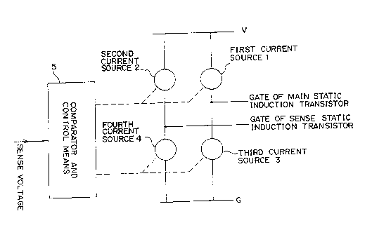
Figure 2A is a block diagram of the present
invention. The present invention is directed to a
control circuit for turning on and off a semiconductor
device comprised of a main static induction transistor
and a sense induction transistor.
A first current source 1 has one end connected to
a power supply (V) and the other end connected to the
main static induction transistor. When turned on,
current source 1 applies bias to the main static
induction transistor.
A second current source 2 has one end connected
to the power supply (V) and the other end connected to
2 ~ 2 ~
the sense static induction transistor. When turned
on, current source 2 applies bias to the sense static
induction transistor.
A third current source 3 has one end connected to
ground (G) and the other end connected to the other
end of the first current source. When turned off,
current source 3 connects the gate of the main static
induction transistor to ground.
A fourth current source 4 has one end connected
to ground (G) and the other end connected to the other
end of the second current source. When turned off,
current source 4 connects the gate of the sense static
induction transistor to ground.
A comparator and control means 5 turns the first
and second current sources on when the semiconductor
device is on, thereby applying bias to the gates of
the main static induction transistor and the sense
static induction transistor. When the magnitude of a
sense voltage resulting from a current flowing through
the sense static induction transistor is higher than a
specific value, the comparator and control means turns
the first and second current sources off and the third
and fourth current sources on.
To turn on the semiconductor device comprised of
the main static induction transistor and the sense
.~
2 ~
-- 7
static induction transistor, comparator and control
means 5 turns on first and second current sources 1
and 2 to apply currents from power supply V to the
gates of the main static induction transistor and
sense static induction transistor. At this point,
third and fourth current sources 3 and 4 are off.
If the load circuit is shorted with the
semiconductor device turned on (and hence a current
flowing through a load circuit), so that an excessive
current flow is produced, the sense voltage will
become higher than the specific value. Upon detecting
that the sense voltage is more than the specific
value, comparator and control means 5 turns first and
second current sources 1 and 2 off. At the same time,
comparator and control means 5 turn third and fourth
current sources 3 and 4 off. Third and fourth current
sources 3 and 4 are adapted to discharge electric
charges stored in the gates of the main static
induction transistor and sense static induction
transistor.
The sense static induction transistor has its
gate current flow produced by second current source 2
and is thus turned on by a constant current
independently of the supply voltage V. That is, the
sense static induction transistor is driven into
~:'
saturation, thereby producing a sense voltage adapted
to exactly detect an excessive current due to a short
of the load. Electric charges stored in the gates of
the main and sense static induction transistors are
rapidly discharged by third and fourth current sources
3 and 4 when the transistors are to be turned off,
thus permitting fast switching operation of the
transistors. This prevents the static induction
transistors from breaking down.
Brief Description of the Drawings
Figure 1 illustrates a circuit arrangement of a
prior art drive circuit.
Figure 2A is a basic block diagram of a
transistor drive circuit of the present invention;
Figure 2B illustrates a circuit arrangement of a
first embodiment of the present invention;
Figures 3A to 3C are detailed circuit diagrams of
the current sources and the current source drive
circuits; and
Figure 4 illustrates a circuit arrangement of a
second embodiment of the present invention.
Detailed Description of the Preferred Embodiments
Referring now to Figure 2B, which illustrates a
circuit arrangement of an embodiment of the present
invention, a load circuit 15 comprises a power supply
2~1~8~6
g
B, a load RL, a semiconductor device 17 having a main
static induction transistor (main SIT) and a sense
static induction transistor (sense SIT), and a
resistor Rs. A common drain of the semiconductor
device is connected to the positive terminal Vcc of
power supply B via load RL. The main SIT has its
source S connected to the negative terminal of power
supply B, while the sense SIT has its source Ss
connected to the negative terminal of power supply B
via resistor Rs. The negative terminal of power
supply B is connected to ground (GND).
When currents flow into gate G of the main SIT
and gate GS of the sense SIT, they are turned on to
thereby produce a current flow through the load. If,
at this point, the gate current of the main SIT is
assumed to be, for example, 300 mA, the gate current
of the sense SIT will be of the order of 5 mA. The
main and sense SITs are driven into saturation, i.e.,
turned on by their respective-gate currents. ~The
maximum current in the on state is substantially
determined by the gate currents of the main and sense
SITs.)
By means of resistor RS connected to the source
of the sense SIT, the current flowing through the
sense SIT can be converted to a voltage which is
8,~
- 10 -
developed across Rs. By use of the voltage across Rs
and the ratio K of the current flowing through the
sense SIT to the current flowing through the main SIT,
the total current, i.e., the drain current of the
semiconductor device, can be found.
A drive circuit 16 for driving load circuit 15
includes current sources 18 and 19, a current source
drive circuit 20 and a control circuit 21, connected
at their ends to the positive terminal Vcc of power
supply B. Control circuit 21 is also connected to a
common terminal of a switch SW. A fixed terminal (On)
of switch SW is connected to the other end of the
current source drive circuit. Upon receipt of a drive
signal from drive signal source S, control circuit 21
connects its moving terminal to its fixed terminal
(On) so that a current Ion is supplied from current
source drive circuit 20 to control circuit 21. With
this flow of current Ion, current source drive circuit
20 turns current sources 19 and 18 on. Current source
18 is adapted to conduct a current IGon, while current
source 19 is adapted to conduct a current IGSon. When
current sources 18 and 19 are on, current sources 22
and 23, which are respectively connected to current
sources 18 and 19, are turned off. (No current flows
through current source drive circuit 25 so that
.
2 ~
- 11 -
current sources 22 and 23 are not driven.)
The common connection point of current sources
18 and 22 is connected to gate G of the main SIT,
while the common connection point of current sources
19 and 23 is connected to gate GS of the sense SIT.
Since current sources 22 and 23 are now off, the
currents supplied from current sources 18 and 19 are
caused to flow entirely into gates G and GS of the
main and sense SITs, respectively. As described
1 0
above, these currents IGon and IGSon are 30
mA, respectively. Since load RL has its end connected
to the power supply and its other end connected to
ground via semiconductor device 17 when it is on, a
current supplied from the power supply flows into the
load.
If load RL should be shorted due to its defect,
an excessîve current will flow. This excessive
current will also flow through the main SIT and the
sense SIT. (At this point the ratio between currents
flowing through the main and sense SITs is K : 1 as in
the prior art.) A voltage is developed across
resistor RS by the current flowing through the sense
SIT for application to overcurrent protection circuit
24.
Overcurrent protection circuit 24 is connected to
.. .
:: .
- 12 -
the positive terminal of a reference voltage source to
provide a reference voltage VRef. The negative
terminal of the reference voltage source is connected
to ground. Overcurrent protection circuit 24 compares
the reference voltage VRef with the voltage across
resistor Rs and, when the voltage across resistor RS
is higher than the reference voltage, applies an off
signal to control clrcuit 21. In response to the off
signal, control circuit 21 places switch SWx in the
ff position. Once this switching is made, the switch
remains in the Off position unless it is reset.
To the terminal (Off) of switch SWx is connected
to current source drive circuit 25. (The other end of
current source drive circuit 25, the other terminals
of current sources 22 and 23 and overcurrent
protection circuit 24 are connected to ground.) When
switch SWx is placed in the Off position, a current
flow is produced in current source drive circuit 25.
When driving current source drive circuit 20, control
circuit 21 connects the common terminal to ground to
thereby connect current source drive circuit 20 to
ground. However, when driving current source drive
circuit 25, control circuit 21 connects the common
terminal to the potential (Vcc) of power supply B to
thereby apply the voltage to the power supply terminal
,
: .
.
:
~$~$
- 13 -
of current source drive circuit 25. At this point
current source drive circuit 25 operates to turn
current sources 22 and 23 on. When switch SWx is
placed in the Off position, current source drive
circuit 20 is left open at its end to stop its
operation. This turns current sources 18 and 19 off.
As a result, the bias to the semiconductor device
becomes zero so that it is turned off. This off can
prevent breakdown of the semiconductor device. When
switch SWx is placed in the Off position, current
sources 22 and 23 are turned on as described above,
thus connecting gates G and GS to ground. The
currents from gates G and GS are caused to flow to
ground. The gates of the main and sense SITs
naturally have stray capacitances. Merely turning
biasing current sources 18 and 19 off will not allow
the main and sense SITs to be turned off immediately
because of electric charges stored in the stray
capacitances. However, the electric charges can be
swept out of the gates by current sources 22 and 23 so
that the main and sense SITs are turned off
immediately.
Because there is no closed circuit in the prior
art, the semiconductor device remains on until the
electric charges are discharged naturally and may
:
.
.: :
.
- : :
- 14 -
suffer breakdown during the discharging period.
According to an embodiment of the present invention,
however, the semiconductor device is driven by current
sources 18 and 19, and not by resistors as in the
prior art. This permits the semiconductor device to
be turned on independently of the magnitude of power
supply voltage Vcc. That is, each SIT can be
saturated so that a proper current is allowed to flow
therethrough even if the power supply voltage is
lowered. Furthermore, even if, in the event of a
failure, an excessive current flows, current sources
22 and 23 are turned off at the same time current
sources 18 and 19 are turned off. This allows
electric charges stored in the gates to be discharged
immediately, thus turning the semiconductor device off
quickly.
Figure 3A illustrates detailed circuit
arrangements of current sources 18 and 19 and current
source drive circuit 20. Current sources 18 and 19
have substantially the same configurations as follows.
Transistors Q10 and Q6 have their collectors connected
to the positive terminal Vcc of power supply B and
their emitters respectively connected to gates G and
GS of the main and sense SITs via resistors R5 and R3.
Transistors Q8 and Q4 have their collectors connected
~3~
- 15 -
to the positive terminal Vcc of power supply B and
their emitters connected to bases of transistors Q10
and Q6~ respectively. Transistor Q7 has its emitter
connected to the positive terminal Vcc of power supply
B and its collector connected to the base of
transistor Q8 and the collector of transistor Qg.
Transistor Q2 has its emitter connected to the
positive terminal Vcc of power supply B and its
collector connected to the base of transistor Q4 and
the collector of transistor Q5. The bases of
transistors Qg and Q5 are connected to the bases of
transistors Q10 and Q6' respectively. The emitters of
transistors Q9 and Q5 are respectively connected to
gates G and GS via resistors R4 and R2.
In current source drive circuit 20, a resistor R1
has one end connected to power supply B and its other
end connected to the bases of transistors Q7 and Q2.
A transistor Q1 has its emitter connected to power
supply Vcc and its base connected to the other end of
resistor R1 and the emitter of transistor Q3.
Transistor Q3 has its collector connected to ground
and its base connected to the collector of transistor
Q1 and a fixed terminal (On) of switch SWx.
Transistors Q1 to Q3 and Q7 are PNP transistors, while
the remaining transistors are NPN transistors.
. 1'
- . ;:
$ ~ :~
- 16 -
Transistors Q6 and Q10 have a larger chip area than
transistors Q5 and Qg so that most of the currents
flowing through gates G and GS flow through
transistors Q6 and Q10~ This will be described later.
When switch SWx is placed in the On position, the
On terminal is placed at ground potential with the
result that transistor Q3 is turned on and thus a
specific current flows through resistor R1. With a
flow of current through resistor R1 the base
potentials of transistors Q1' Q2 and Q7 become lower
than their emitter potential so that they are also
turned on. Thus, supply voltage Vcc is supplied to
the bases of transistors Q4 and Q8 so that they are
also turned on. This turns on transistors Q5, Q6' Q9
and Q10~ These transistors form current mirrors.
Since
I cos ~ I ca9 - I cql
I cab - ~ k 2 - 1 ) I cas
I calo- ( k , - 1 ) I caq
I Con = I caq ~~ I CO I o = k I I ca
I CSon= I cas ~ I co~ = k z I cal
It should be noted herein that transistor Q10 has an
emitter area which is tk1 - 1) times that of
2 ~
- 17 -
transistor Qg and transistor Q6 has an emitter area
which is (k2 - 1) times that of transistor Q5.
Furthermore, resistor R4 has a value of (kl - 1) times
that of resistor 5, while resistor R2 has a value of
(k2 - 1) times that of resistor R3. (Resistors R2,
R3, R4 and R5 are provided for negative feedback to
make each of kl and k2 approximate its respective
desired value where transistors Q5, Q6' Qg and Q10
show manufacturing process variations in emitter
area.)
By the action of the current mirrors described
above, when ICQl flows, IGOn and IGSon flow
correspondingly. These specific currents flow into
gates G and GS of semiconductor device 17 to bring the
main SIT and the sense SIT into saturation.
In the above, an embodiment of the present
invention was described in connection with a
semiconductor device in which a current flow is made
from drain to source. Obviously, the present
invention may also be applied to a semiconductor
device in which a current flows from source to drain.
Figure 3B illustrates detailed circuit
arrangements of overcurrent protection circuit 24,
control circuit 21 and switch SWx. Overcurrent
protection circuit 24 comprises a comparator CMP.
:.
.. ..
. ~ . , .
.:
2 ~
- 18 -
Comparator CMP has its noninverting input connected to
reference voltage VRef and its inverting input
connected to voltage Vs across resistor Rs.
Comparator CMP makes a comparison between these
voltages and produces a high-level output when VRef >
Vs (normal state) and a low-level output when VR~E _
Vs (overcurrent state). The output of comparator CMP
is coupled to the clock input of a flip-flop FF in
control circuit 21.
Control circuit 21 is comprised of a NAND gate
NAND and a flip-flop FF. Flip-flop FF is a D-type
flip-flop and has its output Q connected to an input
of NAND gate NAND. When the power supply is turned
on, flip-flop FF is reset by a reset signal RST so
that its output Q goes high. With this output Q, NAND
gate NAND is enabled to invert a signal from input
signal source S for application to switch SWX. That
is, a high-level signal from signal source S is
inverted to a low-level and vice versa.
The output of NAND gate NAND is connected to each
of control terminals of analog switches AW1 and AW2
and the connection point of AW1 and AW2. Analog
switch AW2 is turned on when its control terminal goes
high and is turned off when it goes low. In contrast
with analog switch AW1, analog switch AW1 is turned on
': '
2 ~ 2 ~
-- 1 9 --
when its control terminal goes low and is turned off
when it goes high.
When the output of NAND gate NAND goes low,
analog switch AW1 is turned on, while analog switch
AW2 is turned off. Thus, the on terminal On of switch
SWX is rendered low in potential. This allows current
source drive circuit 20 described above to drive
current sources 18 and 19, thereby turnil~g
semiconductor device 17 on. When the output of NAND
gate NAND goes high, on the other hand, analog switch
AW2 is turned on, while analog switch AW1 is turned
off. As a result, the off terminal (Off) of switch
SWX goes high. This allows current source drive
circuit 25, described above, to drive current sources
15 22 and 23 so that semiconductor device 17 is turned
off. That is, in the normal state, semiconductor
device 17 is turned on or off according to the level
of the input signal from input signal source S.
When voltage Vs applied to comparator CMP goes
higher than reference voltage VRef, on the other hand,
comparator CMP produces a low-level output. In
response to a transition of the output of comparator
CMP from high-level to low-level (from normal state to
overcurrent state), the flip-flop takes a high-level
input at its D terminal so that its output Q goes low.
,
,;
2 ~
- 20 -
When the output Q of the flip-flow goes low, NAND gate
- NAND is disabled so that its output remains high
independently of the signal from signal source S.
This allows current source drive circuit 25 to
operate, with the result that semiconductor device 17
is always turned off. To sum up the above operation,
semiconductor device 17 is turned on and off by the
input signal from signal source S in the normal state,
while it is turned off when an overcurrent state is
1 o detected .
Figure 3C illustrates another circuit arrangement
of control circuit 21. In this control circuit, flip-
flop FF in control circuit 21 of Figure 3B is excluded
and the output of comparator CMP is directly coupled
to NAND gate NAND instead. With flip-flop FF included
as in Figure 3B, once an overcurrent state occurs,
current flow is stopped. In Figure 3C, once an
overcurrent state is detected, NAND gate NAND is
disabled. That is, when comparator CMP detects VRef _
Vs, the NAND gate is disabled to allow switch SWX to
operate current source drive circuit 25. Thus,
semiconductor device 17 is turned off so that current
flow through the load is stopped. When the current
flowing through the load becomes zero, comparator CMP
produces an output at high level (normal state) again.
-: . : . .~ .:
, : .
- 21 -
In this case, when the signal from input signal source
S goes high, current source drive circuit 21 operates
so that semiconductor device 17 is turned on again to
make a current flow through the load. If the load is
abnormal due to a short, an overcurrent will flow
through the load again to repeat the above operation.
This repeat depends on the loop delay time. By making
the on time of the semiconductor device short when the
load is abnormal, it is possible to prevent the
semiconductor device from breaking down even if an
abnormality, such as a short, occurs in the load.
Figure 4 illustrates a circuit arrangement of a
second embodiment of the present invention. In this
case, semiconductor device 30 is of oppcsite polarity
to semiconductor device 17 described above. Thus,
currents flow in the opposite direction to that in the
first embodiment. The same operation will be
performed if each of the circuits is made to be of
opposite polarity to its respective corresponding
circuit.
As described above, since biases are applied by
current sources even if power supply voltage varies,
substantially constant currents IGSon and IGon are
supplied and a sense gain is never lowered.
If two independent current sources were composed
- 22 -
of discrete components, a complex circuit arrangement
would be needed to compensate for variations in
component characteristics. ~s with the embodiments of
the present invention, if the current sources are made
of semiconductor device drive circuits of 1 chip, the
two independent current sources can be made of simple
circuits because variations in characteristics of
components which are placed close to each other are
small. In addition, the outputs of the two
independent current sources are connected together,
and a drive circuit applicable to a normal three-
terminal transistor may be implemented.
According to the present invention, as described
above, where a semiconductor device having a main SIT
and a sense SIT is used as a switch for driving a
load, when a shorted state is caused by a defect of
the load, a sense current can be detected
independently of the magnitude of a power supply
voltage and the semiconductor device can be turned off
to prevent its breakdown.