Note : Les descriptions sont présentées dans la langue officielle dans laquelle elles ont été soumises.
2019~21
German Patent Application P 39 22 977.7
filed July 12, 1989
Texas Instruments Deutschland GmbH
TID-Case 13586
Our file: T 4664 DE
---
Trimmlng circu1t and trimmlng method performable
uslng such a tr1mmlng c1rcult
_ _ .
~he inventlon relates to a tr1mming circult for settlng a
deslred value of an electrical component and a method for
adjusting an electrical parameter of an assembly by connect-
ing an electrical component with adjustable value uslng suchan 1ntegrated tr1mmlng c1rcult.
Uses exlst ln electronlcs ln whlch assembl1es must ~e
adjusted by changlng the value of an adjustable component.
26 In the adjustment or balanclng operaclon the adjustable com-
ponent is set to a value whLch in cooperation with the
assembly to be adjusted sets an electrical parameter to a
desired value in sald assembly. For example, the assembly
to be adjusted may be the resonant c1rcuit of d tranSmltter
output stage with which for the purpose of the adjusting a
trimming capac1tor is connec~ed 1n parallel ~nich ln tne
balanclng operation lS set to a value such that a deslred
resonant frequency of the resonant circuit 1S achieved. The
exact balancing 15 of great importance in particular when
with a small transmitting power a relatively large range
2 2019921
1 is to be achieved, i.e. an optimum energy irradiation. The
connection of external components to the assembly to be
adjusted is undesirable when the smallest possible space
requirement is desired which can only be satisfied when if
possible all the components are accommodated in an integrated
circuit. Also, connection of external components usually re-
quires the adjusting operation to be carried out by means
of mechanical interventions which is time-consuming and
therefore undesirable.
The invention is based on the problem of providing a trimm-
ing circuit of the type mentioned at the beginning which can
be made in the form of an integrated circuit and in which
the value of the component to be connected to an external
assembly for an adjusting or balancing operation can be set
solely by applying electrical signals. Furthermore, a
trimming method is to be provided with the aid of which
by using the trimming circuit to be provided an electrical
parameter of an assembly can be set in simple manner to a
desired value. To solve this problem the trimming circuit
according to the invention is characterized in that the com-
ponent is made up of a plurality of subcomponents which are
connected in parallel with each other and the values of which
are in a predetermined relationship to each other and that
into a supply line to each subcomponent at least one elec-
trically programmable field-effect transistor is inserted
which via a control gate terminal can be put permanently
into a conductive state or a nonconductive state.
The trimming method according to the invention
is characterized in that into each supply line to a sub-
component a further electrically programmable field-effect
transistor is inserted. An alternative solution of the
trimming method according to the invention resides in that
in the trimming circuit all the subcomponents and the refer-
ence component are rendered effective in that the field-effect
3 2019921
l transistors inserted into their supply lines are put into
the conductive state, that the trimming circuit is connected
to the assembly and the actual value of the electrical para-
meter to be adjusted and the deviation thereof from a
desired value are determined, that the reference component
is rendered ineffective by blocking the field-effect trans-
istor inserted into the supply line thereof, that the change
of the electrical parameter of the assembly caused by render-
ing the reference component ineffective is measured, that
from the measurement result the magnitude of the value of
the subcomponents which is to be rendered effective to
change the electrical parameter of the assembly to be
adjusted fromthe actual value to the desired value is cal-
culated and that the field-effect transistors are blocked
in as many supply lines to the subcomponents as is necess-
ary to reach the calculated value of the subcomponents to
be rendered ineffective.
In the trimming circuit according to the invention the sub-
components forming the component are integrated into a semi-
conductor substrate which also contains the electrically
programmable field-effect transistors. By applying corres-
ponding control signals to said field-effect transistors the
subcomponents can be specifically rendered effective and in-
effective so that the total value of the subcomponents canthereby be set. The component made up of the subcomponents
rendered effective then effects the setting of an electri-
cal parameter to the desired value in the connected assembly.
Further advantageous developments of the trimming circuit
according to the invention are set forth in subsidiary
claims 2 to 5.
The trimming method according to the invention permits an
exact and rapidly performable trimming operation using the
4 2019~21
1 trimming circuit according to the invention; the use of the
reference component makes it possible to compensate process
influences on the values of the subcomponents which can
fluctuate as regards their exact values.
An alternative solution of the method according to the in-
vention is set forth in claim 7.
An embodiment of the invention will now be ex-
plained in detail with the aid of the drawing, the single
Figure of which shows a schematic circuit diagram of the
trimming circuit according to the invention.
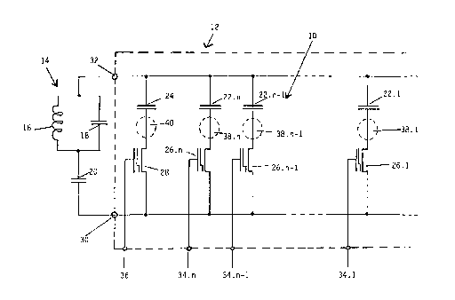
The trimming circuit 10 illustrated in the drawing is part
of an integrated circuit 12 which is shown schematically in
the drawing by a dashed outline. The integrated circuit 12
is for example the output stage of a low power transmitter
in a transponder which is part of an identification system
in which objects to be identified are each provided with
their own transponder which can be activated with the aid
of an interrogation device and stimulated to transmit an
identification code group.
Connected to the integrated circuit 12 is a resonant circuit
14 comprising a coil 16 and two capacitors 18, 20. The coil
16 forms an antenna coil which irradiates the signal to be
transmitted. To obtain the best possible irradiation and
thus the greatest possible range of the irradiated signals
the resonant frequency of the resonant circuit 14 must be
adapted as exactly as possible to the transmitted frequency.
This can be achieved with the trimming circuit 10.
The trimming circuit 10 includes a plurality of integrated
capacitors 22.1 - 22.n which as subcomponents together form
a component which is connected to the resonant circuit 14
2019921
1 for adjusting the resonant frequency thereof. The capacitor
24 is a subcomponent like the capacitors 22.1 - 22.n but
serves a special purpose which will be explained hereinafter.
A field-effect transistor 26.1 - 26.n, 28 is inserted into
each supply line or lead to each of the capacitors 22.1 -
22.n and 24. These field-effect transistors are electrically
programmable field-effect transistors, i.e. field-effect
transistors which by applying a corresponding control signal
to their control gate terminal can be put either into the
nonconductive state or into the conductive state. Said
transistors include a non-connected gate electrode which
is referred to in English technical usage as "floating gate".
The mode of operation of such transistors is generally known
and need not be explained in detail here. The capacitors
22.1 - 22.n are binarily weighted. In the concrete example
of embodiment 7 of these transistors are present which have
consecutively the values lC, 2C, 4C, 8C, 16C, 32C and 64C.
"C" is the capacitance of the smallest of these capacitors.
The capacitor 24 has in the example of embodiment the value
8C. Due to this binary weighting the total value of the
capacitors 22.1 - 22.n can be set to any value between lC
and 127C by rendering effective or ineffective with the
aid of the field-effect transistors 26.1 - 26.n. This total
value plus the value of the capacitor 24 can be connected
in parallel to the capacitor 18 of the resonant circuit 14.
In fabrication of the integrated circuit 12 in the course
of the testing as preparation for the subsequent use all the
transistors 26.1 - 26.n and 28 are put in the conductive
state which means that all the capacitors 22.1 - 22.n and
24 are effective and form a total capacitance corresponding
to the sum of the partial capacitances. After connection
of the resonant circuit 14 to the terminals 30 and 32 of the
integrated circuit 12 the following steps are carried out
to adjust the resonant frequency.
~ .. , '. '
6 201992~
1 Due to production tolerances the absolute capacitances of
the capacitors contained in the integrated circuit cannot
be exactly defined. Since however all the capacitors are
made with the aid of the same process steps they also have
the same production tolerances and this ensures that the
relative relationships defined by the geometry of the capa-
citors are correct. This means in other words that the
capacitance of the capacitor 22.n corresponding to the
aforementioned binary weighting is 64 times as great as the
capacitance of the transistor 22.1.
In a first step of the adjusting method the resonant fre-
quency with which the resonant circuit 14 oscillates when
all the transistors of the trimming circuit 10 are effected
are measured. To determine which capacitors must be ren-
dered ineffective in order to obtain a change of the reso-
nant frequency from the actual frequency to the desired fre-
quency the capacitor 24 is first rendered ineffective by
blocking the field-effect transistor 28 contained in its
supply line. As indicated above, said capacitor 24 as
regards its capacitance is in a fixed ratio to the capacitor
22.1; its capacitance is 8 times as great as the capacitance
of the capacitor 22.1. Rendering the capacitor 24 ineffect-
ive leads to a change of the resonant frequency of the reson-
ant circuit 14, i.e. to an increase because the total capa-
citance which lies in parallel to the resonant circuit 14
is reduced. From the simple oscillation equation of the
resonant circuit 14 it is possible to calculate from the
change resulting from disconnection of the capacitor 24 the
capacitance change which is necessary for changing the
resonant frequency of the resonant circuit 14 from the actual
value to the desired value. The calculation can for example
show that a change of 65C is necessary to give the desired
frequency change. This means that the field-effect transis-
tor 26.1 and the field-effect transistor 26.n must be moved
to the nonconductive state so that the capacitor 22.1 and
7 2019921
1 capacitor 22.n, which together have a capacitance of 65C,
are rendered ineffective. After blocking these two field-
effect transistors 26.1 and 26.n the capacitors of the trimm-
ing circuit 10 have exactly the total capacitance which sets
the resonant frequency of the resonant circuit 14 to the
desired value.
Because of the use of the electrically programmable field-
effect transistors in the supply lines to the capacitors of
the trimming circuit it is only necessary to apply switch-
ing signals to the control inputs 34.1 to 34.n and 36 once
because the switching states of the field-effect transistors
26.1 - 26.n and 28 are retained even when the switching
signals are no longer applied.
In the embodiment of the trimming circuit described it is
assumed that the resonant frequency of the resonant circuit
14 without parallel connection of the capacitors of the
trimming circuit is under all circumstances higher than the
desired frequency to be achieved. With the aid of the
trimming circuit the resonant frequency can then be reduced
until the desired frequency is reached.
In a further embodiment it would also be possible to put the
field-effect transistors 26.1 - 26.n and 28 into the non-
conductive state before the actual use so that initially
all the capacitors 22.1 - 22.n and 24 are ineffective.
During the adjusting operation in this embodiment the field-
effect transistor 28 is then first put into the conductive
state so that the capacitor 24 becomes effective and the
frequency change which results from the effectiveness of the
capacitor 24 in the resonant circuit 14 is determined. It is
then possible to calculate from this frequency change which
capacitance must be connected in parallel to the resonant
circuit 14 to obtain the desired value of the resonant fre-
quency, whereupon the corresponding capacitors 22.1 - 22.n
201992~
1 ~re rendered effective by setting the corresponding field-
effect transistors 26.1 to 26.n contained in their supply
lines to the conductive state with the aid of switching
signals.
In the application of the trimming circuit described above
in the output stage of a transmitter relatively high voltage
peaks can occur at the capacitors 22.1 - 22.n and 24 and
consequently problems regarding the dielectric strength may
possibly arise. To overcome these problems additional elec-
trically programmable field-effect transistors 38.1 - 38.n and
40 which are connected in series with the respective field-
effect transistors 26.1 - 26.n and 28 may be inserted into
the supply lines to the capacitors in each case at the point
shown by a dashed-line circle. In the course of the final
test of the integrated circuit 12 these additional field-
effect transistors are put into the conductive state so that
they do not have any influence on the trimming method out-
lined above. They merely reduce the voltage load of the
individual components lying respectively parallel to the
resonant circuit 14.
It is pointed out that the trimming circuit described may
contain instead of the capacitors 22.1 22.n and 24 resis-
tors which can be rendered effective or ineffective to adjustan assembly in which the adjustment can be achieved by
parallel connection of a specific resistance. The trimming
process would then take place exactly as outlined above in
the case of adjusting the resonant frequency of the reson-
ant circuit 14.
, . . ...