Note : Les descriptions sont présentées dans la langue officielle dans laquelle elles ont été soumises.
` 2020~9
PHN 12.975 1 16.08.1989
'Television system for diqital trans~ission of picture signals.
A. Back~round of the invention
A~ Eield_of_~be_inyçnt gn
The invention generally relates to a television
transoission syste~ comprising a transnitter station, which includes an ;~
encoding station, and co~prising a receiver station, which includes a
decoding station, for transmitting picture signals in a digital format
Y}a a transmission mediu~. Hore particularly, the invention relates to
a television transmission syste~ of the type in which redundancy~
reducing encoding is effected in the encoding station and redundancy-
restoring decoding is effected in the decoding station.
Such a television transmission syste- ~ay form part of a
television broadcasting syste~, in which case the encoding station forms
part of the television broadcasting transmitter and each TV receiver
includes a decoding station. The trans-ission mediu- iY the at-osphere
in this case. Such a television transDission system may also be a video
recording syste~, in which case the transmission mediu~ is, for example,
a video tape or a co~pact disc.
~i~ 20 ;
2~_~çsç~i~t Qn-Q-f-~-h~ iQ~
As is generally knownj ! a~television picture is co pletely
determinod~by three picture slgnals. These may be the three pri~ary
colour slqnals R, G, ~ or, which is the sa~e, one lu inance signal Y and
two colour difference signals U and V, also referred to as I and Q.
:~
~hese colour difference signals will hereinafter be referred to as
CHR(1) and CHR(2).
As is also generally known, a sampling frequency iY :
30 asYociated with each digital signal. This means that the samples -~`constitutinq this digital signal occur at this sampling frequency. In
practice, each sample is represented by a number comprising a given
. . .
2020~09
. .
PH~l 12.975 2 16.08.1989
number of bits. For the current digital television transmission systems
the sampling frequency is standardized at 13.5 MHz. The sampling is
performed in such a manner that 720 samples for each of the three
picture signals are obtained for each visible line of the picture. If
the number of visible lines per television picture is assumed to be 576
and the number of bits per sample is assumed to be eight, approximately
10 Hbits are to be transmitted for each television picture. At 25
pictures per second this means a bit rate of approximately 250
Mbit/second. This requires a transmission channel having a bandwidth of
approximately 125 MHz. In practice, such transmission channels are
usually not available. For example, in a video recorder the transmission
channel in this case formed by the write head, the tape and the read
head has a maximum bandwidth of 30 MHz.
To be able to transmit a television picture in a digital
format through a transmission channel having a considerably limited
bandwidth, it is co~mon practice (see for example References 1 and 2 in
the next section C) to use the luminance signal Y and the two colour
difference signals CHR(1) and CHR(2) as picture signals, instead of the
three primary colour signals. This choice is made because the luminance
signal has a considerably larger signal-energy content than each of the
two colour difference signals. If this luminance signal is sampled for
its transmission at a frequency fyl each of the two colour difference
signals can be sampled at a lower frequency fcNR. More particularly,
fy is an integral ultiple N of fcHR. A5 already stated, fy z 13.5
~Hz and N is chosen to be 2 for the current television trans~ission
syste-s. Consequently, the bit rate can be reduced to a value of ~ .
approximately 167 Mbit/second, which is 2/3 of the original bit rate.
Reference 1 states that N ay even be chosen to be 3 without serious ~ -;
loss of quality. It also states~that the number of colour difference
samples to be transmitted can be halved without any noticeable loss of
quality by transmitting during one of two successive picture lines the
samples of one of the two colour difference signals. For example, during ~ -
a first picture line the samples of the colour difference signal CHR(1)
are transmitted only and during a subsequent picture line the samples of ~ -;
the colour difference signal CHR(2) are transmitted only. The so-called
vertical decimating filters with which this is realised (referred to as
~Vertikales Chrominanzfilter~ in Reference 1) and which have a
2~2~09
PHN 12.975 3 16.08.1989
decimation factor R which in this case is equal to two, thus produce
digital auxiliary colour difference signals CH(1) and CH(2). The -
encoding station of this known transmission syste- has also an input
circuit which receives the picture signal Y and the two auxiliary colour
difference signals CH(1) and C~(2) and which has two auxiliary picture
signal outputs at which a first and a second auxiliary pictùre signal
occur. More particularly, the first auxiliary picture signal is equal to ~
the luminance signal and the second auxiliary picture signal is ~ ; constituted by a time-division multiplex of the samples of the one
auxiliary colour difference signal CH(1) of the one picture line and the
saaples of the other auxiliary colour difference signal CH(2) of the
subsequent picture line.
For a further bit rate reduction the sa-ples of the
luminance signal Y occurring at the first auxiliary picture signal
output are also applied to a first redundancy-reducing encoding circuit
and the samples of the multiplex signal occurring at the second
auxiliary picture signal output are also applied to a second redundancy-
reducing encoding circuit. ~oth redundancy-reducing encoding circuits
are differential pulse code modulators.
Each redundancy-reducing encoding circuit produces a
channel signal which is applied to the transmission edium by eans of
an output circuit. Shese signals applied to the transmission medium will
be referred to as trans-ission medium signals.
It is to be noted that it is known per se to realise
redundancy reduction in a way other than by means of differential pulse
code odulation, for exa-ple, by performing a Q*Q forward transfor-. In
that case all those samples of a picture signal forming one complete
picture are considered as ele-ents (pixels) of a atrix. This matrix is
divided into sub-matrices of Q by Q matrix ele-ents and this sub--atrix
is written as the su- of Q2 orthonor~al Q*Q basic matrices each with
its own weighting factor (coefficient). In such a redundancy reduction a
part of the said weighting factors is transmitted instead of the ~ ~-
original sa-ples. ;~
Yet another ~ethod of realising redundancy reduction is
the use of differential pulse code modulation co-bined with a Q*Q
forward transform. Such a co~bination is also referred to as hybrid
encoding (see, for example Reference 3).
``` 2020~9
PHN 12.975 4 16.08.1989
For regaining the original picture signal~ Y, CHR(1) and
CHRt2) the receiver station of the television transmission system
described in Reference 1 has an input circuit which can be coupled to
the transmission medium and which regenerates the original two channel
S signals, starting from the infor~ation (trans~ission medium signals) -
present at this transmission medium. Each channel signal is applied in a
decoding station to an individual redundancy-restoring decoding circuit
whose operation is inverse to the said redundancy-reducing encoding
circuits and each of them supplies a regenerated local auxiliary picture
signal. These two auxiliary picture signals are converted by ~eans of an
output circuit into the original lu-inance signal Y and the original two
auxiliary colour difference signals CH(1) and CH(2), which signals occur
at separate outputs of this output circuit. The two auxiliary colour
difference signals are subjected to a vertical interpolation operation
so as to generate the original colour difference signals CHR(1) and
CHR(2).
As is known, much research has been done in the field of
high-definition tele~ision in the last few years. High-definition
television pictures co-prise, for example 1250 lines of which 1152 are
visible and carry picture information. Moreover, the aim is a higher
horizontal resolution in combination with a higher aspect ratio, namely
16 : 9; in the current television pictures this ratio is 4 : 3. It is to
be noted that the aspect ratio of a television picture is the ratio
between the horizontal and the vertical dimension of the picture.
Trans-ission of picture signals for such pictures in a digital for-at
implies in the first place that the reguired sampling frequencies ust
be chosen to be considerably higher than is co~mon practice in the
current television transmission systems. For obtaining, in~ÇE ~lia a
sufficiently high horizontal resolution, a sampling frequency of 5i4 MHz~
is reco~ ended. If such a high sampling frequency were used in the
television tran ission system described in Reference 1, it would Dean
that the one redundancy-reducing encoding circuit receives samples
~namely those of the lu~inance signal) at a rate of 54 MHz and the other
at a rate of 18 MHz. - ~ -
When using such a transmission systea in consumer
apparatus such as, for example digital video recorders, the aim will be -~
a high degree of integration. If the integrated circuits are for~ed in
-
: `
PHN 12 975 5 16 08 1989
the currently ost advanced integration technique, which is known under
the'name of CMOS, a high internal processing rate, namely up to 30 MHz
is possible at a high integration density When integrating the ~ 'redundancy-reducing encoding circuit receiving samples at a rate of 5
MHz, this internal processing rate of 30 MHz is absolùtely
insufficient It is to be noted that it is possible to integrate an
encoding circuit by means of CMOS techniques and to realise an internal
processing rate of 54 MHz or more, but this is at the expenise of the
integration density In fact, this density considerably decreases with
an increasing processing rate The required chip surface and hence the
price of the chip increase considerably
arv of thç,,,,inyçntion
The invention has for its object to provide a television
transmission system of the type described hereinbefore in relation to
Reference 1 and which is particularly suitable for transmitting high-
definition television pictures, permitting a high degree of integration
and being particularly suitable for digital video recording '
To this end the television trans-ission system according
to the invention i5 characterized in that
- each of the two redundancy-reducing encoding circuits is adapted to
perfor- a two-di~ensional Q*Q forward transforn;
- the input circuit of the encoding circuit is adapted to perfor- a
distribution operation in which the luminance signal DY and the two
auxiliary colour difference signals CH(1) and CH(2) are partitioned into
lu~inance groups and chro~inance groups, respectively, with Q saoples ~
per group, each ti-e of an even nuober of successive luminance groups ,,~"
and an even number of chro-inance groups a first half of said nu-ber of ~ ,
lu~inance groups and~a first,lhalf of said number of chrominance groups,
are applied in a tiDe-division multiplex format to the first auxiliary
picture signal output and the other half of said number of luminance ~ ~
groups and the other half of said number of chrominance groups are , ,
applied in a time-division multiplex format to the second auxiliary ~ -
picture signal output; ` ,
- the redundancy-restoring decoding circuit is adapted to perfor- a two-
di~ensional Q*Q inverse transform;
- the output circuit of the decoding station is adapted to perfor- a ' ,
- ;!: . .; ~ : ,' . "' . . ' ' ;
2~2~09
... .:
PHN 12.975 6 16.08.1989
rearrangement operation which is inverse to the distribution operation.
~ y using the measures according to the invention it is
achieved that both groups of samples of the luoinance signal and groups
of samples of each of the two auxiliary colour difference signals are
distributed between the two auxiliary picture signal outputs. As a
result, the rate at which samples occur at each of these outputs can be
adapted to the internal processinq rate of the redundancy-reducing
encoding circuits. More particularly it appears that N can be chosen to
be 4 for hiqh-definition television pictures and it is co~mon practice
to perform 8*8 forward transfor~s in the redundancy-reducing encoding
circuits. Since one half of the total number of groups is applied to the
one auxiliary picture signal output and the other half is applied to the
other auxiliary picture signal output, the sa~ples can be presented to
each encoding circuit at a rate of approxioately 27 HHz. Each redundancy-
reducing encoding circuit now supplies a channel signal at a bit rate ofapproxi~ately 100 MHz. It is true that this bit rate will usually be too
high to enable the two channel signals to be trans-itted through a
co~mon transmission channel, but two separate transnission channels, one
for each channel signal, are a~ply sufficient for this purpose. Since
each channel signal comprises luminance information as well as colour
infor-ation of a television picture, a drop-out of a transnission
channel, for example, because one of the two read heads in a video ~ ;
recorder has become defective, will still yield a recognizable colour
television picture.
A very practical nu ber of successive luminance groups is
2N. After this nu-ber of lu~inance groups is applied to the distribution
circuit, this circuit has also received 4/R chrominance groups.
The distribution between the two auxiliary picture signal
outputs will preferably be effected as regularly as possible. This can
particularly be achieved by applying the successive luminance groups
alternately to the first and to the second auxiliary picture signal
output.
.-
C. References
35 1. Aufwandsaroen DPCM-Coder f~r die TV-Verteilung mit 72 Mbit/s; ~ ~-
P. Neuhold;
Nachrichtentechnische Zeitschrift, Vol. 41, No. 9,
PHN 12.975 7 16.08.1989
September 1988, pp. 506-511.
2. Adaptive coding of monochro~e and colour images;
W.H. Chen, C.H. Smith;
IEEE Transactions on Communmications, Vol. COM-25,
No. 11, November 1977, pp. 1285-1292.
3. Videobild auf der Datenleitung;
P. Vogel;
Funkschau No. 26, 16 December 198B, pp. 60-63,
4. One-dimensional linear picture transformer.
R. WoudsDa, D.C.H. Chong, B.T. Mc Sweeney, S.M. Borgers,
E.A.P. Habraken;
European Patent Application No. 0,286,184
p. Ex~natiop ~ the inV~e~tion
D~ Hrief_descE'ption_Qf_the_Figyres
" ,~
Fig. 1 shows diagrammatically the television transmis~ion ; ,;;~
syste~ according to the invention in the for- of a video recorder;
Figs. 2, 3 and 4 show diagrams to explain the operation
of the television transmission system of Fig. 1; '~
Fig. 5 shows diagra~matically the structure of a
distribution circuit for use in the television transmission system of "'
Fig. 1;
~ Figs. 6, 7 and 8 show so~e control circuits for
controlling,the distr,ibution,circuit shown in Fig. 5.
~ ' ,
~2~ Qener3a__tryctyrç_Qf_the_teleyision_system
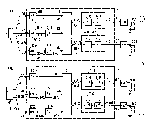
Fig. 1 shows diagram~atically a video recorder provided ' , '
with the television transmission system according to the invention. It ~;
co-prises a transmitter station TR including an encoding station A and a
receiver station REC including a decoding station B. The encoding
station A has three inputs AO, A1, A2 or receiving a luminance signal
, 9
PHN 12.975 8 16.08.1989
Y, a colour difference signal CHR(1) and a colour difference signal
CHR(2), respectively, which are supplied by a picture signal source PS,
for example a video camera. It will hereinafter be a~su~ed that each
television picture comprises two successively occurring fields whose
composite picture lines are interlaced. The encoding station A has also
two outputs A3, A4 at which serial bit currents occur which will be
referred to as channel signals Z1(n) and Z2(n). These channel
signals are converted by ~eans of separate modulation circuits MOD into
transmission medium signals which in their turn are recorded
simultaneously but separately on a ~agnetic tape TP ~ separate write
heads C(.), for example on separate tracks.
To regain the original picture signals, the decoding
station B has two inputs D3, ~4 which are connected to separate read
heads D(.~ via separate demodulation circuits HOD 1. These read
heads can be coupled to the oagnetic tape TP in such a way that they
convert the information which is present on this ~agnetic tape into the
original transmission ~edium signals which lead to local channel signals
Z'1(n) and Z'2tn) after demodulation in the demodulation
circuits MOD-1, which channel signals correspond to the original
channel signals Z1~n) and Z2(n) as are supplied by the encoding
station A. This decoding station D also has three outputs BO, B1, B2 at
which locally generated versions Y', CHR~(1) and CHR~(2) of the
original picture signals Y, CHR(1) and CHR(2) occur. These local picture
signals are applied to a monitor M.
In the encoding station A the three picture signals Y,
CNR~1) and CHR(2) are saopled in A/D converters 1(1), 1(2), 1(3),
respectively, at suitably chosen sampling frequencies fy and fcHR
and the sa~ples thus obtained are converted into, for example 8-bit PCM
words, hereinafter generally referred to as picture signal samples but
ore particularly the sa~ples of the lu~inance signal Y being referred
to as luminance samples and those of each of the colour difference
signals being referred to as colour difference sanples. It will be
assumed that fy = 54 MHz and fcHR = 13-5 MHz so that the ratio N =
fy/fcHR = 4. These A/D converters thus supply the digital picture
signals DY, DCHR(1) and DCHR(2), respectively. The digital colour
difference signals DCHR(1) and DCHR(2) are subjected to a vertical
deci-ation operation in vertical deci~ating filter devices 2(1) and
~.. ~. . .
: .
.
-` 2~2~9~9
PHN 12 975 9 16 08 1989
2(2) which have a decimation factor of R = 2 They suppress all colour
difference samples of one of two successive picture lines of a field and
thus supply digital auxiliary colour difference signals CH(1) and CH(2)
The digital luminance signal and the two digital
auxiliary colour difference signals are applied to inputs 3(1), 3(2) and
3l3), respectively, of a distribution circuit 3 which has two auxiliary
picture signal outputs 3(4) and 3(5) This distribution circuit will be
further described in section D~3) In this respect it is to be noted
that this distribution circuit supplies auxiliary picture signals AP(11
and AP(2) at each of its auxiliary picture signal outputs
A redundancy-reducing encoding circuit 4( ) is connected
to each auxiliary picture signal output 3(4), 3(5) This circuit is
constituted by a cascade circuit of a transformer 5( ) and an encoder
6( ) The transformer 5( ) is adapted to perform a two-dimensional
forward Q*Q transform, for example, a Discrete Cosine Transform
(abbreviated DCT) It is co-mon practice to choose Q to be equal to
eight This will also be the case in this description Many examples of
such a transformer have been described in literature; see, for example
Reference 4 Generally it can be noted that such a transformer each time
converts a two-dimensional catrix of 8*8 picture signal samples into a
atrix of 8*8 so-called coefficients The encoder 6( ) receives the 64
coefficients thus obtained and encodes the- in a suitable way; for
example, in the way as has extensively been described in Reference 2 and
each time converts a ~atrix of coefficient~ into a bloc~ of serial
25 bits The redundancy-reducing encoding circuits 4( ) thus for-ed thus ~ -
supply the previously entioned channel signals Z1(n) and Z2(n)
In the decoding station B the local channel signals
Z~1(n) and Z~2(n) supplied by the demodulators MOD-1 are
applied to redundancyrrestoring decoding circuits 7( ) They are both
constituted by a cascade circuit of a decoder 8( ) and a transformer
9( ) The decoder each ti~e reconstructs a matrix of 64 coefficients
from the received local channel signals This matrix is subjected in the
transfor-er 9( ) to a two-dimensional inverse 8*8 transform (in this
case, for exa-ple an inverse Discrete Cosine Transform) so that each
~atrix of coefficients is converted into a matrix of 8*8 picture signal
samples These are applied as local auxiliary picture signals AP~
and AP~(2) to inputs 10(4) and 10(5) of a rearrangement circuit 10
-: 2 ~
PHN 12.975 10 16.08.1989
which performs an operation which is inYerse to the operation performed
by the distribution circuit 3. This rearrangement circuit thus supplies
at its outputs 10(1), 10(2), 10(3) a local digital luminance signal
DY~, a local digital auxiliary colour difference signal CH~(1) and a
local digital auxiliary colour difference signal CH~(2),
respectively. The two local digital auxiliary colour difference signals
are subjected in vertically interpolating filter devices 11t.) to a
vertical interpolation operation, where the interpolation factor R is
egual to the decimation factor, i.e. two in this case. This operation is
thus inverse to the vertical decimating operation and reconstructs for
each field all non-transmitted colour difference samples of one of two
successive picture lines. They thus supply the local digital colour
difference signals DCHR~(1) and DCHR~(2). The local digital
luminance signal DY~ as well as the local digital colour difference
signals DCHR~(1) and DCHR~(2) are applied to respective D/A
converters 12(.) and converted into local analog picture signals Y', -~
CHR~(1) and CHR'(2) which are applied to the onitor M. ~ -
~-3l-~-hç--di-s~i-b-utiQ~-çi~çyit
Fig. 2 shows diagraDatically so~e ti-e diagrams to
explain the operation of the distribution circuit 3 for distributing
picture signals of high-definition television pictures. As already
noted, such television pictures conprise 1250 picture lines. It will be
assumed that each television picture of this type is supplied by the
video source PS in the foro of two successive interlaced fields, with
each field comprising 625 picture lines. In Fig. 2 the successive
picture lines of the two successive fields Rm and Rm+1 of a picture
are denoteq at A by means of blocks. These picture lines are enu~erated
L1 to L625 for each field and have a period T (= 32 ysec). As is known,
not all picture lines of a field comprise picture signals. It will be
assumed that only the picture lines L1 to L576 of a field comprise ~ ~
picture signals and these picture lines will be referred to as the ~ `
active picture lines of a field. The other picture lines of a field will
35 be referred to as passive picture lines. These active picture lines bear ~`
the inscription AC at A in Fig. 2. At ~ in Fig. 2 those active picture
lines whose luminance samples are applied to the input 3(1) of the
2 ~ 9
PHN 12.975 11 16.08.19B9
distribution circuit are denoted by means of the inscription Y. At C
those active picture lines whose colour difference samples of the colour
difference signal CH(1) are applied to the input 3(2) of the
distribution circuit are denoted by means of the inscription CH(~) and
at D those active picture lines whose colour difference saoples of the
colour difference signal CH(2) are applied to the input 3(3) of the
distribution circuit are denoted by means of the inscription CH(2). It
is to be noted that in the case considered the inputs 3(2) and 3(3) of
the distribution circuit only receive colour difference samples of the
odd picture lines.
Each picture line (period 32 ~sec) has a length which
corresponds to 1728 ~ampling periods Ty = 1/fy~ Each active picture
line comprises an active line section and passive line sections. The
active line section is the section where picture signals may occur,
whereas no picture signals but, for example, line-synchronizing pulses,
field-synchronizing pulses and fra~e-synchronizing pulses may occur in
the passive sections. Normally, the active line section begins and ends
a first and a second predetermined period, respectively, after the
occurrence of the line-synchronizing pulse. It will be assumed that the
first-mentioned period corresponds to 160 periods Ty and the said
second period corresponds to 160 + 1408 periods Ty~ In other words, `
the active line section has a length of 1408 sampling periods Ty~
Each picture line bearing the inscription Y of the time
diagram shown at B in Fig. 2 symbolizes a series of 1728 luminance
samples, with only those luminance samples of the active sections of the
active lines in principle having a value which is unequal to zero. Such
a picture line is shown at a smaller scale in the time diagram E. The
1728 luminance samples of this series are partitioned into 1728/Q = 216
groups of Q = 8 luminance sa~pies each by the distribution circuit.
Those groups which comprise in principle non-zero lu~inance samples of
the active secSion of an active picture line will be referred to as
luminance groups. In the time diagram E these luminance groups
successively bear the inscriptions Y1 to Y176 and the other groups
which comprise in principle luminance samples which are zero
successively bear the inscriptions 1 to 040. It is to be noted that
such a group occurs in a time interval To = 8 Ty~ -
Each picture line with the inscriptions CH(1) and CH(2)
:
202~al~9
PHN 12.975 12 16.08.1989
of the time diagrams C and D symbolizes a series of 432 colour
difference samples which occur at a rate of 13.5 MHz, while only those
colour difference sanples of the active sections of the active lines in
principle have a value which is unequal to zero. These picture lines are
~hown at a smaller scale in the time diagrams F and G. Each one of such
a series of 432 colour difference samples is partitioned into 432/Q = 54
groups of Q = 8 colour difference samples each by the distribution
circuit. Those groups which comprise in principle non-zero colour
difference samples of the active section of an active picture line will
10 be referred to as chrominance groups. Time diagrams F show these -~
chrominance groups which are successively denoted by CH(1)1 to ~ :
CH(1)44, while the other groups are denoted P1 to P10. In a
corresponding manner, time diagram G shows the chrominance groups which
are successively denoted by CH(2)1 to CH(2)44 and the other groups
which are denoted S1 to S10.
The distribution circuit now applies four luminance
groups and one chrominance group of 2~ = 8 successive luminance groups
and 41R = 2 chrominance groups to each of the two auxiliary picture
signal outputs 3(4) and 3(5). More particularly it applies the
successive luminance groups of a picture line alternately to the one and
to the other output 3~4) and 3(5), respectively, and one chrominance
group is applied to each output each time after 2N(= 8) lu~inance groups
have been distributed. All this is shown diagra3matically in the time
diagrams H and I of Fig. 2. More particularly the time diagram H shows
the groups which occur at auxiliary picture signal output 3(4) and the
time diagram I shows the groups which occur at auxiliary picture signal
output 3(5). Due to this distribution of the luminance and chrominance ~- -
groups between the two auxiliary picture signal outputs, each of these
outputs is available for a time interval 2To so as to transfer the
eight picture signal samples of a group to the transformer 4(.). All
picture signal samples now occur at a rate of 27 MHz at the aoxiliary
picture signal outputs 3(4) and 3(5). This is half the rate at which the
luminance sa-ples occur at the input 3(1). It is true that this is twice
the rate at which the colour diference sa~ples occur at the outputs of
the A/D converters 1(2) and 1(3), but this rate of 27 MHz is below the
permitted rate of 30 MHz which is prescribed by the transformer 4(.~.
The above-mentioned distribution of the groups of picture
,~
202~90~
PHN 12.975 13 16.08.1989
signal samples can be effected in different ways while taking the above
considerations into account, the distribution of the luminance groups
between the two outputs being independent of the distribution of the
chrominance groups.
The different distribution possibilities for the
luminance groups will be further described with reference to Figs. 3A to
3D. More particularly each of these Figs. 3A-3D shows a field of a
television picture. This field comprises 576 visible picture lines Li
with i = 1, 2, 3, ... 576 and each picture line is partitioned into 176
luminance groups Yr with r = 1, 2, 3, ... 176.
The distribution of the luminance groups between the two
auxiliary picture signal outputs 3(4) and 3(5) can now be effected in
the way shown in Fig. 3A such that the luminance groups having an odd
ordinal number r of each picture line are applied to the auxiliary
picture signal output 3~4) and those having an even ordinal number r are
applied to the auxiliary picture signal output 3(5). In Fiqs. 3A-3D
tbese outputs are denoted by the reference numerals 4 and 5 for the sake
of brevity. In other words, if a luminance group Yr of picture line Li
is applied to auxiliary picture signal output 3(5), the numeral 5 is in
the relevant box. If it is applied to auxiliary picture signal output
3(4), the nu~eral 4 is in the relevant box. This distribution of the
luminance groups will be referred to as first luminance distribution
mode and is denoted Y-mod 1 in Fig. 3A.
A second luminance distribution mode is shown in Fig. 3B
and denoted by Y-mod 2. The luminance groups are distributed between the
two outputs in such a way that the output 3(4) each time receives the
even luminance groups and output 3(5) only receives the odd lu~inance
groups.
In a third!luminance distribution mode the luminance
30 groups of two successive pictures are subjected to the first luminance `' !i~
distribution ode Y-mod 1 for the one picture and the luminance groups
of the other picture are subjected to the second luminance distribution
mode Y-mod 2.
A fourth luminance distribution mode is shown in Fig. 3C
and denoted by Y-mod 4. In this mode each time Q/2 = 4 successive
picture lines of a field are considered as a block of picture lines. The
576 visible lines of a field can be partitioned into 144 of such picture
2~2~9
PHN 12.975 14 16.08.1989
line blocks. Fig. 3C shows these picture line blocks which are denoted
by B1, ~2, ... B144. Furthermore, the luminance groups of the picture
line blocks B1, ~3, ... having an odd ordinal nu~ber are subjected to
the first luminance distribution mode Y-mod 1 and the luminance qroups
S of the picture line blocks B2, B4, ... having an even ordinal nu~ber are
subjected to the second luminance distribution mode Y-mod 2.
A fifth luminance distribution mode is shown in Fig. 3D
and is denoted by Y-mod 5. This luminance distribution mode differs from
the fourth luminance distribution node in that the picture line blocks
~ 3, ... with an odd ordinal nu~ber are now subjected to the second
luminance distribution mode Y-mod 2 and the picture line blocks B2, B4
... with an even ordninal number are subjected to the first luminance
distribution mode.
In a sixth luminance distribution mode one picture of two
successive pictures is subjected to the fourth luninance distribution
mode Y-mod 4 and the other picture is subjected to the fifth lu~inance
distribution mode Y-mod 5.
The choice of the above-described luminance distribution
modes in a concrete case is determined by the picture quality desired at
the receiver end on the one hand apd by the price of the system on the
other hand. The influence of the different luminance distribution modes
on the picture quality in the receiver station ay be best exa-ined by ~!7`',, ', ~' ,''',,'
checking to what extent the picture quality decreases if one of the two
inputs 10(4) or 10(5) of the rearrangement circuit 10 in the decoding
station B (see Fig. 1) does not receive a signal. Let it be assumed that
this i5 input 10(5). Since this input 10(5) receives all luminance
groups which occur at the output 3(5) of the distribution circuit, it
means that all those luminance groups which are denoted by 5 in Figs. 3A-
3D do not contribute to the~picture on monitor M. In the case of thè
first or the second luminance distribution mode this eans that the
picture exhibits vertical dark stripes. When using the third luminance
distribution mode Y-mod 3, these dark stripes disappear because both the
luminance groups with an even ordinal number and those with an odd
ordinal number, though at half the picture frequency, are applied to the
input 10(4) of the rearrangenent circuit. When using the fourth
luminance distribution mode Y-mod 4 shown in Fig. 3C or the fifth -
luminance distribution mode shown in Fig. 3D the picture on uonitor M ~ -
2~20~
PHN 12.975 15 16.0~.1989
will exhibit dark areas, like the distribution of tbe dark fields on a
chessboard. These dark areas disappear by using the sixth luminance
distribution mode in which all luminance groups are applied once to the
input 10(4) of the rearrangement circuit each time after two pictures.
As already noted, the distribution of the chrominance
groups can be performed independently of the selected luminance
distribution mode. The different distribution possibilities for the
chrominance groups will be further described with reference to Figs. 4A
to 4F. Likewise as in Figs. 3A to 3D, each of these Figs. 4A to 4F shows
a field of a television picture comprising 576 visible picture lines Li
with i = 1, 2, ... 576 and each odd picture line is partitioned into 44
chrominance groups CH(1)S with s = 1, 2, 3, ... 44 and 44 chrominance
groups CH(2)S (see also Fig. 2).
Since in the case considered a chrominance group CH(2)S
occurs simultaneously with the occurrence of a chrominance group
CH(1)S, these groups will be considered as a unit. Such a unit will be
denoted by the symbol shown in Fig. 4G, which symbol is in the form of a
rectangle partitioned into two triangles by means of a diagonal. Either
the numeral 4 or the numeral 5 will be placed in each of these
triangles. The numeral in the triangle to the left of the diagonal
denotes the output 3(.) of the distribution circuit to which output the
chrominance group CH(1)S is applied and the nu~eral in the triangle to
the right of the diagonal denotes the output 3(.) of the distribution
circuit to which output the chro~inance group CH(2)S i8 applied.
The distribution of the chrominance groups between the
two outputs 3(4) and 3(5) can now be performed in the manner shown in
Fig. 4A such that the chrominance groups CH(1)S of each relevant A .
picture line are applied to output 3(4) and the associated chrominance
groups CH(2)s are applied to the output 3(5). This distribution of the
chrominance groups will be referred to as first chrominance distribution
mode and will be denoted by CH-mod 1.
A second chrominance distribution mode is shown in Fig.
4a and will be denoted by CH-mod 2. It differs from the first
chrominance distribution mode in that the chrominance groups CH(1)
3~ are now applied to the output 3(5) and the chrominance groups CH(2)S
are applied to the output 3(4).
In a third chrominance distribution mode the chrominance
.
202~909
PHN 12 975 16 16 08 1989
groups of the one picture of two successive pictures are each time
subjected to the first chrominance distribution mode CH-mod 1 and those
of the other picture are subjected to the second chro-inance
distribution mode CH-mod 2
S A fourth chrominance distribution mode i5 shown in Fig
4C and will be denoted by CH-~od 4 Each time the chrominance groups
CH(1)s having an odd ordinal number s are applied to the output 3(4)
while simultaneously the chrominance groups CH(2)S having an odd
ordinal number s are applied to output 3(5) Conversely, the chrominance
groups CH(1)S having an even ordinal number s are applied to output
3(5), while simultaneously the chrominance groups CH(2)S having an
even ordinal number s are applied to output 3(4)
A fifth chrominance distribution mode CH-mod 5 is shown
in Fig 4D It differs from the fourth chrominance distribution mode CH- ~
15 mod ~ in that the chrominance groups CH(1)S having an odd ordinal ;
number are now applied to output 3(5) and those having an even ordinal
number are applied to output 3(4), while the chrominance groups CH(2)s
having an odd ordinal number are applied to output 3(4) and those having
an even ordinal number 5 are applied to output 3(5)
In a sixth chro-inance distribution mode CH-mod 6 the
chrominance groups of the one picture of two successive pictures are
each time subjected to the fourth chrominance distribution oode CH-mod 4
and those of the other picture are subjected to the fifth chrominance
distribution mode CH--od 5
A seventh chrominance distribution mode CH--od 7 is shown
in Fig 4E In this mode each time Q (= 8) successive picture lines of a ~;
field are considered as an auxiliary picture line block A TV picture
can be partitioned into 72 of such auxiliary picture line blocks In
Fig 4E these blocks are,denoted by BB1, BB2, BB72 The chrominahce
30 groups of the auxiliary picture line blocks having an odd ordinal number ~i
~BB1, BB3, BB71) are subjected to the fourth chrominance
distribution ode CH-ood 4 and the chrominance groups of the auxiliary
picture line blocks having an even ordinal number (BB2, BB4 B~72)
are subjected to the fifth chrominance distribution mode CH--od S ;
An eighth chrominance distribution ode CH-mod 8 is shown
in Fig 4F and it differs from the seventh chrominance distribution mode
CH-mod 7 in that the auxiliary picture line blocks having an odd ordinal
. :.
`"
`
--: 202~0~
PHN 12 975 17 16 08 1989
number (BB1, B~3 B~71) are now subjected to the fifth chrominance
distribution mode CH-mod 5 and the auxiliary picture line blocks having
an even ordinal number (BB2, B~4, B3~72) are subjected to the fourth
chrominance distribution mode CH-~od 4
S In a ninth chrominance distribution mode CH-mod 9 the
chrominance groups of the one picture of two successive pictures are
each time subjected to CH-mod 7 and those of the other picture are
subjected to Cff-~od 8
The best choice of the above-described chrominance
distribution modes in a concrete ca~e again depends on the desired
picture quality on the one hand and on the price of the system on the
other hand As far as the picture quality is concerned, the remarks ade
in connection with the different luminance distribution modes are
applicable If one of the two local auxiliary picture signals AP~(1)
or AP~(2) is absent at the receiver end (see Fig 1), the best
possible picture quality on onitor M is achieved when using the sixth
lu-inance distribution mode Y--od 6 and the ninth chrominance
distribution mode CH-mod 9
An embodiment of the distribution circuit 3 is shown in ~Y
20 Fig 5 This distribution circuit is particularly adapted to perform the ~`
lu-inance distribution mode Y-mod 6 and the chrominance distribution
mode CH-mod 3 For distributing the lu-inance ~amples, two buffer
circuits 3 01(1) and 3 01(2) are connected to the input 3~1), each of
which circuits may be in the for- of a fifo They are controlled by
write pulses clwy which occur at the sampling frequency fy~ by write-
enable signals WE(1) and WE(2), by read-enable signals RE(1) and RE(2)
and by read pulses clry which will be assumed to occur at a frequency
of 27 HHz Of the luminance samples occurring at a frequency of 54 MHz -~at the input 3(1) Q z,8 $amples will alternately be written in the!one
fifo and 8 samples will be written in the other fifo under the control
of the write pulses clwy and the write-enable signals WE( ) In the
embodiment shown the read-enable signals RE( ) are constantly positive, ~ `
which means that they do not block the reading of samples from the ~ -
fifo In response to each read pulse clry a luminance sample is read ;~
from a fifo The output of fifo 3 01(t) is connected to the input
- 3 31(1) of a multiplexer circuit 3 30(1) and the output of fifo 3 01(2) `~` -
is connected to the input 3 31(2) of a multiplexer circuit 3 30~2) ~
2~90~9
PHN 12.975 18 16.08.1989
The write-enable signals WE(.) can be generated by means
of the control circuit shown in Fig. 6. This circuit more particularly
comprises a modulo-8-counter 3.10 which receives the write pulses (54
MNz) clwy and which supplies a toggle pulse to a so called toggle flip-
flop 3.11 whenever a predetermined count occurs, while the output signalof said flip-flop represents, for example the write-enable signal WE(1)
and a version of the write-enable signal WE(2) inverted by means of an
inverter 3.12. To ensure that these write-enable siqnals have the
correct value at the start of each picture line and the start of each ~ -
picture, this toggle flip-flop is of the set reset type, for example,
the Signetics SN 7473. This flip-flop not only reacts to the toggle
pulses supplied by the modulo-8-counter 3.10 but also to so-called set-
reset pulses which it receives at a set-reset input SR. In the
embodi~ent shown these set-reset pulses are supplied by an OR gate
3.13. It receives the output pulses via a first input from a toggle
flip-flop 3.14 which is controlled by a ~odulo-4-counter 3.15 which
receives pulses H occurring at the line freguency which is approximately
equal to 32 kHz for high-definition television pictures with 1250 lines
per picture. This modulo-4-counter 3.15 supplies a toggle pulse for -
toggle flip-flop 3.14 whenever a predetermined count occurs. Yi~ a
second input OR gate 3.13 receives output pulses from a toggle flip-flop
3.16 which receives frame-~ynchronizing pulses FP (25 Hz~ at its input.
In this way it is achieved that the toggle flip-flop 3.11 is set to a
defined starting position each time after four picture lines of the ~ ~
25 field and each time after two fields. This control circuit further ~ ~ ;
comprises a frequency divider 3.17 which receives the write pulses
clwy (54 MHz) and divides them by a factor of 2. It thus supplies
clock pulses Cl, the read pulses clry and further write pulses
clw~y which occur at a frequency of 27 MHz.
For distributing the colour difference ~amples of the two
auxiliary colour difference signals CH(1) and CH(2), two registers
3.04(1), 3.04(2) and 3.04(3), 3.04(4) are connected to each of the
inputs 3(2) and 3(3), respectively, of the distribution circuit 3.
Particularly, registers of the type having a 3-state output, for exa~ple
the Signetics SN 74374 can be cho~en for this purpose. Although such
registers are generally known, it is to be noted that they can be
controlled by means of a logic output enable signal OE(.) in such a way
'"''''`'"~,.'''";''.'''"'~-'' '`'' ` '
2~2~09
PHN 12.975 19 16.08.1989
that the output can assume the loqic value ~1~ or the logic value ~0~,
for example, if OE(.) has the logic value ~1~, or if the internal
resistance, viewed from the output, assumes a very high value, for
example if OE(.) = O. The latter property provides the possibility of
directly interconnecting outputs of such registers so as to obtain a
wired OR circuit. More particularly the outputs of the registers
3.04(1) and 3.04(3) are interconnected and are connected to the input
3.32(1) of the multiplexer circuit 3.30(1), while the outputs of the
registers 3.04(2) and 3.04(4) are interconnected and are connected to
the input 3.32(2) of multiplexer circuit ~.30(2).
The registers 3.04(.) are not only controlled by the
output enable signals OE(.) but also by write pulses clwch which occur
at the sampling frequency fchr = 13-5 MHz. In this way it is acbieved
that a colour difference sample occurring at the input 3(2) or 3~3) is
taken up in the relevant registers under the control of a write pulse
clwch but is only available at the output of that register whose logic
output enable signal has the value ~1~ at that moment. In the embodiment
chosen these logic output enable signals only change their value with
the frame freguency. For the sake of completeness an embodiment of the
control circuit reguired for generating the output enable signals is
shown in Fig. 7. It comprises a toggle flip-flop 3.20 which receives the ~ -~
frame-synchronizing pulses FP occurring at a freguency of, for e~a-ple
25 Hz. The output signal of this flip-flop 3.20 is directly applied to
the registers 3.04(1) and 3.04(4) as logic output enable signals OE~
and OE(4). The version of this output signal which is logically inverted
by means of the inverter 3.21 is applied as logic output enable signals
OE~2) and OE(3) to the registers 3.04(2) and 3.04(3), respectively.
The ~ultiplexer circuits 3.30(.) have a ~imilar
construction and each~of them~comprises a first, or luminance register
3.33(.) and a second, or chrominance register 3.34(.) both of which are
in the form of 3-state output fifos. The outputs of these two registers
are connected to the output 3(4) or 3(5) of the distribution circuit.
The input of the lu~inance register 3.33(.) is connected to the input ;
3.31(.) of the multiplexer circuit and has a capacity which is at least
equal to the number of luminance samples of the active section of an
active picture line. This lu~inance register 3.33(.) is controlled by
write pulses clw~y which, likewise as the read pulses clry, ocsur
,
. , .
,
- 2~2~9
PHN 12 975 20 16 08 1989
at a frequency of 27 HHz; by a write-enable signal WEy indicating
which one of the presented luminance samples can be read in the
register; a read-enable signal REy indicating when luuinance sa~ples
can be read from this luminance register 3 33( ) The rate at which
luminance samples are read fro~ this luminance register is deter~ined by
those read pulses clry which occur at a rate of 27 MHz and which pass
an AND gate 3 35 controlled by the read-enable signal REy The write- -
enable signal WEy activates the write operation of the luminance
register 3 33( ) only for those luminance samples which are taken from
the active section of an active picture line The read operation is
alternately activated by the read-enable signal REy during thirty-two
clocX pulse periods of clock signal cl and is deactivated during the
subsequent Q = eight clock pulse periods, so that four lu~inance groups
are consecutively applied to the output 3(4)
The input of the chrominance register 3 34( ) is
connected to the input 3 32( ) of the multiplexer circuit and has a
capacity which is at least egual to the number of colour difference
~amples taken from the active section of a picture line This
chrominance register is controlled by write pulses clw~ch which
occur at a rate of 13 5 MHz; by a write-enable signal WECh which,
likewise as the write-enable signal WEy of lu-inance register 3 33( )
indicates which one of the presented colour difference samples can be ~ -
read in the chro inance register Further-ore, this chro~inance register ~ ~ ;is controlled by a read-enable signal RECh indicating when colour
difference samples can be read from this chro~inance register 3 34( )
The rate at which this is effected is determined by read pulses clr
which occur at a rate of 27 MHz and which are derived from the read- ~ -
enable signal RECh and the 27 MNz clock signal cl by means of an AND
gate 3 36 More particularly,,only those colour difference samples whiah
are taken from the active section of an active picture line are written
in the chrominance register 3 34( ) The read-enable signal RECh
enables the chrominance register 3 34( ) to read Q = eight colour
difference samples (corresponding to one chrominance group) of this
chrominance register whenever the read operation of the luminance
35 register is deactivated and to apply them to the output 3(4) or 3(5) ~ -
Consequently, it is achieved that four luminance groups and one
chrominance group alternately occur at the output 3(4) as well as at the
. ~ .
~. . ~, ..
' ~ -i: .'
- 2 a 2 ~ a o s
PHN 12.975 21 16.0~.1989
output 3(5) of this distribution circuit.
The different read-enable and write-enable signals for
these registers 3.33(.) and 3.34(.) can be generated by means of a
control circuit which may have a construction as shown in Fig. 8.
This control circuit comprises a counter circuit 3.40
which receives the clock pulses cl (27 MHz) and which is reset whenever
a line-synchronizing pulse H occurs. This counter circuit supplies a - -
~r~
logic ~1~ at the counts 160/2 = 80 to 784 (= 1408/2+80). At the other
counts it supplies a logic value ~0~. This counter thus defines the ~ ,~
10 previously aentioned active section of an active picture line. This -
control circuit further comprises a line counter circuit 3.41 which
receives the line-synchronizing pulses as counting pulses which is each
time reset by a fra~e-synchronizing pulse FP. This counter circuit 3.41 : ~'
supplies a logic value ~1~ as long as its count corresponds to active
15 picture lines. These are the picture lines 1 to 576 of each field in the ~- ' `
case of high-definition television. The logic values supplied by the two , ~ ~ -
counter circuits 3.40 and 3.41 are applied to an OR gate 3.42 whose
output conveys a logic signal which is applied as a write-enable signal ; ~, ;
WEy to the luminance register 3.33(.) and which is applied as a write-
enable signal WECh to the chrominance register 3.34(.). The read-
enable signals RE~. and RECh are derived fro- a modulo-40-counter
circuit 3.43 which receives the clock pul~es cl (27 ~Hz) as counting
pulses and is reset by each frame-~ynchronizing pulse FP. This modulo-40-
counter circuit 3.43 supplies a logic value ~1~ for each of the counts 0
to 31 and it supplies the logic value ~0~ for each of the count~ 32 to
39. These logic values are directly applied as a read-enable signal
REy to the luminance register 3.33(.), while the version inverted by
the inverter 3.44 is applied as a read-enable signal RECh to the ~ -;
chrominance,~register 3.34(.).~
'
E _Gg~gral_Eemarks ,
An embodiment of the distribution circuit 3 has
extensively been described in the previous section, which embodiment can
be used in the encoding station A of Fig. 1. An embodiment of the
rearrangement circuit, which can be used in the decoding station B of
Fig. 1, can be obtained by inverting the signal direction in the
20209~9 ~ ~
PHN 12.975 22 16.08.1989 -
distribution circuit shown in Fig. 4 and by giving the write and read-
enable signals the status of read and write-enable signals,
respectively.
It is also to be noted that it has been assumed in the
foregoing description that each picture comprises two interlaced
fields. If this were not the case, each picture should be partitioned
into picture line blocks of eight picture lines each for performing the
luminance distribution mode Y-mod 6 and, for example the modulo-4-
counter 3.15 which is used in the control circuit shown in Fig. 6 should
be replaced by a modulo-8-counter.
In Fig. 2 it is shown at C and D that the inputs 3(2) and
3(3) of the distribution circuit only receive the colour difference
samples of the odd picture lines. It will be obvious that an alternative
choice is to apply only the colour difference samples of the even
picture lines to these inputs. As is stated in Reference 1 it may be
possible to apply the colour difference samples of the colour difference
signal CH(1) of, for example the odd picture lines to input 3(2) and the ~ i~
colour difference samples of the colour difference signal CH(2) of the
even picture lines to input 3(3), or conversely.
Figs. 2, 3, 4 and 5 are based on the assumption that the
ratio N between luminance and chrominance sampling frequency is equal to
four. However, a different value may be taken for this ratio N. For
example the value N = 2 or the value N ~ 3 frequently occurs in
practice.
Furthermore the said Figs. 2, 3, 4 and 5 are based on the
assumption that the decimation factor R is egual to two. However, this
decimation factor may alternatively be equal to 1. It may also have a -~ -
value which is larger than two. If R = 1, the vertical decimating means
only consist of direct connections between the outputs of the A/D ! ' ' ~-
converters 1(2) and 1(3) and the corresponding inputs 3(2) and 3(3),
respectively, of the distribution circuit 3. The vertically
interpolating means 11(1) and 11(2) may then al~o be for~ed by direct ~ ~-
connections between the outputs 10(2) and 10(3) and the inputs of the
corresponding D/A converters 12(2) and 12(3), respectively. ~ ~.
If, for example N = 3 and R = 1, the distribution circuit
is adapted to distribute each time six luminance groups and 4
chrominance groups between the two outputs 3(4) and 3(5). Each output
,. 20200as
PHN 12.975 23 16.08.1989
then receives three such luminance groups, with, for exa~ple one
chrominance group each time between two such luminance groups.
,,".~ ~, "
~', ''~ .''-' ,. ;'
;~