Note : Les descriptions sont présentées dans la langue officielle dans laquelle elles ont été soumises.
BC9-89-033 - 1 - 2023618
PERSONAL COMPUTER PROCESSOR CARD INTERCONNECT SYSTEM
FIELD OF THE INVENTION
This invention relates to improvements in data
processing systems of the type in which various
components, including a microprocessor, are mounted on
printed circuit boards (PC8 s). More particularly, it
relates to an improved personal computer system unit
design in which a processor card having a microprocessor
and other related components mounted on a PCB, is mounted
on a planar board by means of a novel interconnect system
that facilitates installation and replacement of the
processor card.
BACKGROUND OF THE INVENTION
The history of personal computer design is
characterized by continuing technological improvements not
only in the microprocessors but also in associated
components. A desirable objective is to provide a system
unit design that is stable and in which the various
components or assemblies thereof, can be replaced by the
user with upgraded, improved components without requiring
the user to have any technical skill or use special tools.
Processor cards have been suggested in which the
microprocessor and related components are mounted on a PCB
that can be plugged into a mating connector on a planar
board. Yet such a design may not be suitable for some
current technology.
Current technology includes personal computers having
thirty-two bit wide data and address paths which causes
the processor card to have a multiplicity of wires and
edge contacts. In order to plug such a card into a mating
edge connector~ a relatively great force is needed to
spread the mating contact arms and develop the necessary
wiping force required to establish good electrical
contact. Such great force needs to be very carefully
.~'
- 2023618
BC9-89-033 - 2 -
applied to the processor card in order not to bend or flex
the card great enough to break a wire or a component.
Another objective of personal computer design is to
provide a relatively low cost unit. As the number of
contacts on a processor card increases, the cost of a
single, mating connector increases non-linearly due to the
high density of the contacts and the cost of building a
long line of contact arms within the necessary close
tolerances.
SUMMARY OF THE INVENTION
One of the objects of the invention is to provide an
improved personal computer system unit having a processor
card mounted on a planar board in such a manner as to
allow a user to readily replace the processor card.
Another object of the invention is to provide a
replaceable processor card adapted to be mounted on a
planar board, the processor card having mounted thereon a
microprocessor, a direct memory access (DMA) controller, a
read only memory (ROM), a memory controller, a bus
controller, and error checking means all of which are
interconnected with printed circuits that terminate in a
multiplicity of edge contacts which mate with
corresponding contact members on the planar board, the
edge contacts being in the many data, address, interrupt,
and control lines extending between the processor card and
planar board.
Another object is to provide a processor card with a
novel interconnect system facilitating installation and
removal of the card.
Another object is to provide a simple, low cost
interconnect system for a printed circuit board having a
multiplicity of contacts spaced along one edge thereof.
~ 2~236~8
BC9-89-033 - 3 -
A further object is to provide a processor card
requiring a relatively great force to plug it into a
connector, with a user operated force amplifying means
that controls the application of the force to the card so
as not to bend or flex the card during installation and
removal.
Still another object is to provide a processor card,
having a large number of edge contacts and mating
connector means, which is low cost while providing a
multiplicity of mating contacts all located within high
tolerances necessary to align and mate with the
corresponding edge contacts.
A still further object is to provide a processor card
having a large number of edge contacts with a novel
inserter/extractor which coacts with a stationary frame
element to not only develop high forces necessary to
install and extract the processor card, but also acts as a
guide to align the processor card during installation and
as a lock to hold the card in place.
Another further object is to provide a novel
connector system for use with a processor card having a
large number of edge contacts, the system using existing
connector designs to avoid having to retool to make an
otherwise larger single connector.
Briefly, in accordance with one aspect of the
invention, the manner in which certain of the above
objects is attained is to provide a processor card
comprising a printed circuit board (PCB) on which are
mounted a microprocessor and such other related components
as are likely to be upgraded or improved. Such components
may include a cache, cache controller, a read-only memory
containing operating system programs, a direct memory
access controller, a coprocessor, error checking circuits,
a bus controller, and a memory controller. The processor
card has one edge along which a multiplicity of closely
spaced contacts are arranged on opposites sides of the
PCB. The contacts carry the many data, address, control,
~ - 2023618
BC9-89-033 - 4 -
power and interrupt signals transmitted between the
processor card and a planar board. Because of the large
number of contacts, the processor card has novel means for
bringing the contacts into precise engagement with mating
edge connectors on the planar board. Two levers are
pivotally mounted on the card and are engageable with
stationary fulcrums mounted on the frame of a personal
computer for generating the high forces needed to engage
and separate the contacts from the mating connector.
In accordance with another aspect of the invention,
the mating connector is formed from two edge connectors
each having the same or approximately the same number of
contacts arms. The two connectors are mounted on the
planar board in very exact, aligned locations, such
connectors being provided with a locating key that is
engageable in a slot along the edge of the processor card
to precisely align and locate the contacts relatively to
the contact arms.
In accordance with still another aspect of the
invention, the levers function as inserter/extractors and
coact with the fulcrums on the frame. Such fulcrums are
further provided with guides that fit into slots into the
levers and are located to guide the edge contacts into the
mating connectors. The levers are provided with means to
"lock" onto the PCB and engage the fulcrums to thereby
hold the processor card in place.
DRAWINGS
Other objects and advantages of the invention will be
apparent from the following description taken in
connection with the accompanying drawings wherein:
Fig. 1 is a schematic block diagram of a processor
card constructed in accordance with the invention;
Fig. 2 is a schematic block diagram of a planar board
constructed in accordance with the invention;
- 2023618
BC9-89-033 - 5 -
Fig. 3 is a exploded, isometric view, with portions
removed, showing portions of the invention;
Fig. 4 is an enlarged end elevation view, with
portions removed, of an edge connector on a planar board,
about to mate with the edge of a processor card;
Fig. 5 is a view similar to Fig. 4 showing the edge
of the processor card mated with the edge connector;
Fig. 6 is an enlarged detail view showing contacts on
the edge of the processor card;
Fig. 7 is a top plan view of a portion of an edge
connector;
Fig. 8 is a front elevational view of a frame
element:
Fig. 9 is an end elevational view of the frame
element shown in Fig. 8, mounted on a frame;
Figs. 10-12 are elevational views showing progressive
relative positions of an actuator and a frame element, as
the processor card is mounted on the planar board; and
Fig. 13 is a perspective view of an actuator.
DETAILED DESCRIPTION
Referring now to the drawings and first to Fig. 1, a
processor card 10 comprises a printed circuit board 12
having surface mounted thereon a plurality of commercially
available components including a microprocessor 14, a math
coprocessor 16, a cache controller 18, a cache memory 20,
a direct memory access (DMA) bus control unit 22, a bus
control 24, a memory controller 26, a read only memory
(ROM) 28, parity checking units 30 and 32, an oscillator
34 and clock generator 36. Preferably, the microprocessor
is a high performance type, such as an Intel 80383
- 2023618
BC9-89-033 - 6 -
microprocessor, having thirty two bit data paths and
providing thirty two bit addressing capability. The
remaining components are selected in conventional fashion
for their compatability with such microprocessor. A
plurality of buffers 38, 40, 42, 44 and 46 are connected
as shown and provide selective isolation or connection
between the circuits allowing different portions to be
concurrently used, e.g., to move data between the
microprocessor and cache while data is being transferred
between an I/0 unit and main memory. All of the above
components are electrically connected to each other as
appropriate by printed wiring circuits in PCB 12 which
terminate at contacts, described below, located along an
edge 48. Such edge is pluggable into edge connectors on
planar board 50 shown in Fig. 2.
The wiring circuits of PCB 12 include a local bus 54
including data, address and control lines 56, 58 and 60
respectively, which interconnect microprocessor 14 with
coprocessor 16, cache controller 18 and cache memory 20,
as shown in Fig. 1. The remaining circuit lines generally
include interrupt lines 62, channel bus lines 64 and
memory bus lines 66. The channel bus lines 64 include
control, data and address bus lines 70, 72 and 74
respectively. Memory bus lines 66 include multiplexed
memory address lines 82, row address strobe (RAS) lines 84
and 86 for memory banks A and B, column address strobe
(CAS) line 88, data bus A and B lines 90 and 92, and a
line 94 for use in error checking via parity check or ECC
checking. Further circuit lines include those needed for
direct memory access and include memory data lines 76,
address lines 78, and control lines 80. For simplicity,
certain miscellaneous lines, such as reset, grounds,
power-on, etc. have been omitted from the drawings.
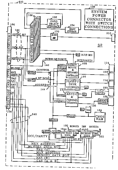
Referring to Fig. 2, planar board 50 comprises a PCB
52 upon which are surface mounted various components that
are interconnected by wiring or circuits in the PCB. Such
components include two processor card connectors 100 and
101 described in more detail below, into which processor
card 10 is plugged for mounting the processor card upon
2~23618
BC9-89-033 - 7 -
the planar board. A plurality of single in-line memory
module (SIMM) connectors 102 are also mounted on PCB 52
for connecting to memory banks 104A and 104B each having
SIMM s thereon forming the system main memory. One or
more expansion connectors 106 are also mounted on PCB 52
for connection to different expansion adapters and options
(not shown) that might be added or incorporated into the
personal computer system. Connector 106 is a commercially
available connector of the type conforming to the above
mentioned Micro Channel architecture, and connectors 100
and 101 are identical thereto but differ in their use as
to what signals or ground lines are connected to the
various elements in each connector.
Also mounted on planar board 50 are an interrupt,
mouse and keyboard controller 108, a floppy disk
controller 110, and an asynchronous and parallel interface
112 connected to a keyboard connector 114, a mouse
connector 116, a diskette connector 118, an asynchronous
connector 120, and a parallel port connector 122, which
allow various I/O devices to be connected into the system.
A system power connector 128 is mounted on PCB 52 for
connection to a plug in power unit that supplies the
necessary power for the system. A CMOS RAM 124 and a
time-of-day clock 126 are also mounted on PCB 52. Also
mounted on PCB 52 are an audio amplifier 130, a card
select feedback 132 and a ready feedback 134. The PCB 52
also has mounted thereon various oscillators to provide
timing signals, and buffers to isolate sections of the
circuitry.
The wiring of PCB 52 interconnects the various
components as shown in the drawing and is grouped into
three groupings, a memory bus 140, a channel bus 142, and
miscellaneous signal lines including interrupt lines 143
all of which are connected to counterpart wiring on PCB 12
through connectors 100 and 101. Tapped off bus 142 is a
planar function bus 144.
Referring now to Fig. 3, the system unit includes a
frame assembly 200 upon which planar board 50 is mounted.
- 2023618
BC9-89-033 - 8 -
Planar board 50 comprises a PCB 52 which is thin, flat,
and rectangular, and has its components surface mounted
thereon on the surface located away from the frame
assembly. Processor card 10 is designed to be mounted
generally perpendicular to PCB 52 and thus the connectors
100 and 101 are located with their mounting grooves
(described below) opening in a direction away from the
planar board. Connectors 100 and 101 are longitudinally
aligned, i.e., they are mounted end to end, with the
adjacent ends being slightly spaced to allow the
connectors to be located with their contact arms correctly
spaced to mate with the edge contacts as hereafter
described. Each expansion connector 106 is mounted on the
planar board parallel to connectors 100 and 101. Memory
connectors 102 are mounted in parallel rows.
As seen best in Fig. 3, PCB 12 is flat, thin and
rectangular. The lower edge 48 is long and straight and
has a first notch 162 therein providing clearance to fit
over the end wall 164 of the adjacent connector 100. A
corner of PCB 12 is notched at 166 to provide clearance
for the opposite end wall of the other connector 101. A
central notch 168 provides clearance to fit over the
adjacent end walls of connectors 100 and 101. A notch
171 provides clearance to fit over key 172 of connector
101. A notch 169 has a tight sliding fit over key 173 of
connector 100 to properly locate PCB 12 relative to
connectors 100 and 101. The keys are in the middle of the
connectors and serve as reference points for positioning
the contact arms in the connectors during the fabrication
thereof. During assembly of the planar board, keys 172
and 173 are used to precisely align and position
connectors 100 and 101 relative to each other. Thus, only
one key 173 and one notch 169 need be used to align the
contacts on the processor card with the contact arms in
the connectors.
The lower edge 48 is beveled at 174 to form a wedge
operative to guide such edge between the rows of contact
arms when card 10 is installed. Spaced along edge 48 are
a multiplicity of contacts 176 located in two rows on
- 2023618
BC9-89-033 - 9 -
opposite sides of PCB 12. The contacts form part of the
wiring or circuits of the PCB and are evenly spaced in
each row with a center to center spacing of .05 inches.
The contacts are very thin and lie substantially flush
with the surface of the PCB. The contacts are accurately
positioned relative to notch 169 so that the notch can be
used to properly align the mating contacts and contact
arms.
.
Referring now to Figs. 4-7, connector 100 has a
generally rectangular transverse cross section and is
composed of an insulating body 178, a multiplicity of
connector pins 182 and a like multiplicity of contact arms
186 connected to such pins. In the preferred embodiment,
connector 100 has one hundred sixty four pins, and PCB 12
has three hundred twenty eight contacts. Connector 100 is
surface mounted on PCB 52 and has a plurality of standoffs
180 that space the body slightly away from the adjacent
surface of PCB 52. Pins 182 extend through PCB 52 and are
reflow soldered thereto to electrically and mechanically
mount the connector on PCB 52. A bifurcated locating pin
184 extends through the PCB and is used to roughly attach
the connector to the board during the assembly/fabrication
process. Contact arms 186 are arranged in two rows
extending along groove 170, the contact arms being
flexible, spring members biased or preloaded into
engagement with abutments 188. The contact arms are bent
or shaped so as to extend into groove 170 whereby the
spacing between adjacent pins in opposite rows (across
groove 170) is less than the thickness of PCB 12. The
contact arms have the same spacing as contacts 176. When
the processor card is installed, the bevel 174 wedges the
contact arms apart against the bias thereof to develop a
wiping force of at least seventy five grams per each
contact/contact arm engagement thereby insuring a good
electrical contact therebetween. Such wiping force is
obviously dependent on the spring constant of the contact
arms and the amount of deflection. The use of two
commercially available connectors is advantageous because
it results in a less expensive design by not requiring any
retooling that would otherwise be required to use a new,
- - 20Z36~8
BC9-89-033 - 10 -
single connector having the necessary number of contact
arms.
As shown in Fig. 3, two frame elements 201, which
form part of the frame assembly 200, are mounted in
positions adjacent the mounted position of processor card
10. Referring to Figs. 8 and 9, each element 201 is
similar so only one need be described. Element 201 is of
sheet metal and has a flat base 202, a fulcrum/latch
member 204 that extends outwardly from the base, and a
guide 206 that also extends outwardly from the base at a
right angle relative to member 204 but spaced therefrom.
As shown in Fig. 3, processor card 10 has two
actuators or levers 210 mounted on opposite corners of PCB
12 on its top edge. The levers function as inserters,
extractors, and latches to facilitate installation and
removal of the card and to lock or latch the card in
position. The levers are identical so only one need be
described in detail. Referring to Figs. 10-13. lever 210
has an elongated body 212 provided at one end with a
handle 214. The other end is specially shaped to coact
with frame element in a manner described in detail below.
Lever 210 has a pivot hole 216 through which a pivot pin
218 extends allowing the lever to be rotated about the
axis of the pin. The pin is press fitted into PCB 12.
The specially shaped end is in the form of an open mouth
having an upper jaw 220 and a lower jaw 222 providing two
fulcrum surfaces 224 and 226. The lower jaw is split or
bifurcated by a slot 228 of a width slightly greater than
the thickness of guide 206 to provide a sliding fit
therewith. Slot 228 and guide 206, when interfitted,
occupy the same radial plane relative to the axis of
rotation of the lever. Pivot hole 216 is located closer
to jaws 220 and 222 than to handle 214 so as to provide
unequal moment arms. Handle 214 is further from the pivot
hole, and hence from the axis of rotation, to provide a
longer moment arm than the length of the moment arm to the
j~ws whereby a force manually applied to handle 214 is
amplified to develop the higher forces necessary to insert
and remove card 10. Lever 210 is a classical class 2
2~2~6~8
BC9-89-033 - 11 -
lever where one end acts as the fulcrum, the pivot pin
located between the ends acts as the load, and the handle
end receives the actuating force. Lever 210 further
includes two parallel, flexible arms 228 that are spaced
apart a distance slightly greater than the thickness of
PCB 12. Two opposed dimples 230 project towards each
other from adjacent sides of arms 228 and are engageable
in holes 232 in PCB 12 to releasably lock lever 210 in
place against the upper edge of PCB 12. To accomplish
this, dimples 230 and holes 232 are located the same
radial distances from the axes of rotation of the levers.
The two frame elements 201 are mounted in positions
close to where the levers 210 will be when the processor
card is installed or mounted on the planar board. The
elements coact with the levers to install and extract the
processor card and therefore act to generally align the
processor card with connectors 100 and 101 at the start of
installation. Guides 206 provide a more accurate aligning
function, they being accurately located relative to
connectors 100 and 101 so that when the levers 210 are
engaged with the guides, PCB 12 is precisely perpendicular
to the planar board and lies in a plane extending in the
direction of movement of the PCB. When thus aligned, the
upper edge of PCB 12 lies directly above connectors 100
and 101 and the forces of the levers acting on the PCBs
are directed downwardly through the plane of the PCB
without introducing any lateral forces that might
otherwise bend the PCB and possibly break some of the
printed circuits therein.
In order to install or mount processor card 10 on
planar board 50, levers 210 are rotated to an open
position wherein they extend above PCB 12 and provide
handles for lifting and guiding edge 48 into connectors
100 and 101. In such position, as best seen in Fig. 10,
jaw 222 is displaced from fulcrum 204 to allow the jaw to
be lcwered past the fulcrum 204. During the process of
lowering, lever 210 is concurrently rotated clockwise as
viewed in Fig. 10. The levers would be moved laterally as
necessary to align slots 228 with guide 206 and thereby
- 20236i8
BC9-89-033 - 12 -
allow the guide to enter the slots as continued rotation
occurs. Such movement causes surface 226 to abut fulcrum
204 on the undersurface thereof. This should occur about
at the point when edge 174 is resting on top of contact
arms 186. Continued rotation of lever 210 forces the
lower edge bevel 174 to wedge the rows of contact arms 186
apart against the bias thereof while lowering edge 48
between the contact arms (Fig. 5). During such lowering,
surface 226 slides on the underside of fulcrum 204 and
passes through the position shown in Fig. 11. Rotation
continues until the underside of body 212 of lever 210
abuts the adjacent top edge of PCB 12, as shown in Fig.
12. As the lever moves into this latter position, arms
228 straddle PCB 12 and the dimples 230 slide thereover
until they move into locking hole 232 in PCB 12. The
dimples are spherical and in conjunction with the
flexibility of arms 230 provide a releasable latch or lock
to hold lever 210 in the latched position. At such point,
surface 222 abuts the underside of fulcrum 206 and thereby
prevents upward movement of PCB 12 until such time as
lever 210 is rotated in the opposite direction. Removal
is accomplished by simply rotating the levers to initially
overcome the force needed to move the dimples from holes
232 and the frictional forces holding the lower edge 48 in
connectors 100 and 101. Such latter rotation brings
surface 224 of the upper jaw 220 into contact with the
upper surface of fulcrum 204 allowing the lever to amplify
the forces manually applied thereto causing such rotation.
Continued rotation will separate PCB 12 from the
connectors allowing the processor card to be lifted away
from the planar board.
It is to be appreciated that the system described
above is advantageous in several ways. First, the system
units may be of two types, a table model and a floor
standing model which allows a variety of different
personal computer models to be made differing in one
aspect by the number of expansion and memory slots.
Second, processor cards using different microprocessors
can have different components mounted thereon to provide
different performance characteristics and a user could
`--BC9-89-033 - 13 - 2023618
readily replace or upgrade the system. Third, the system
can be improved by replacing the memory units with ones of
greater speed or storage capacity, and this can be readily
done at the same time a processor card is replaced.
Fourth, a processor card need not have all the components
shown in the illustrated embodiment. The coprocessor,
cache and its controller, are optional, although their
absence will cause the system to perform at a lesser
level. ECC circuitry can be used in place of the parity
checking. Fifth, since the upgradeable components (i.e.,
the processor card and memory cards) are easily
replaceable, the remaining components provide a stable
design that should be usable for several years.
It is also to be appreciated that many other changes
can be made in the details and arrangements of parts
without departing from the scope of the invention as
defined in the appended claims.