Note : Les descriptions sont présentées dans la langue officielle dans laquelle elles ont été soumises.
- 202~6~1
ELBCTRICAL DOUBLE-LAYER CAPACITOR
1. Technical Field
The present invention relates to an electrical
double-layer capacitor wherein a plural number of
cells are connected in an arbitrary connecting
relation without making them form a high bulk
assembly.
2. Background Art
FIG. 4 shows a conventional electrical
capacitor cell. In FIG. 4, numeral 1 denotes a
collecting electrode, 2 a polarizing electrode, 3 a
separator, 4 a gasket, and C a cell.
The collecting electrode 1 is made, for
example, of a conductive rubber sheet, and the gasket
4 is made, for example, of a non-conductive rubber.
Also, the separator 3, is made, for example, of a
polyethylene porous film.
The polarizing electrode 2 is one which has
been made of active carbon powder formed into a
paste-like matter and impregnated with an
electrolytic liquid (for example, dilute sulfuric
acid). ~As the polarizing electrode of an electrical
double-layer capacitor cell, it is known to use one
which is made into a solid plate-like form by
sintering active carbon powder, and having an
electrolytic liquid impregnated thereinto).
The gasket 4 is made in a tube-like form, and
at the approximately central part of its inside,
there is arranged a separator 3 in such a manner as
to delimit upper and lower parts. Respective
polarizing electrodes 2 fill the spaces above and
below the separator 3, and respective collecting
electrodes are provided in such a manner as to cover
the polarizing electrodes 2 and the gasket 4.
2023631
The gasket 4 is adhered to the collecting
electrode 1 and the separator 3, and the collecting
electrode 1 is contacted to the surface of the
polarizing electrode 2. The above-described adhesion
is carried out by use of an adhesive agent or by heat
melting.
The breakdown voltage of the cell C formed in
such a manner as described above is less than several
V. Therefore, in the case when it is used in a use
requiring higher breakdown voltage, a number of cells
C must be connected in series. Also, when the
capacity is deficient, a number of cells C must be
connected in parallel.
Hitherto, in relation to the technology for
connecting a plural number of cells, have been
proposed a method in which the collecting electrodes
at the part where they become doubled at the time of
laminating are laminated in a single layer (public
report of the Japanese Patent Application Laid-Open
No. 97770/1979), a method of connecting cells in
series by the use of a conductive plate for carrying
the polarizing electrodes of the neighboring cells in
common (public report of the Japanese Patent
Application Laid-Open No. 162218/1980), and a method
for providing a predetermined plural number of cells
(for example, 4 pieces) in one body in a connecting
relation previously determined (public report of the
Japanese Patent Application Laid-Open No.
194417/1984.
However, in the above-described respective
technologies, there still are some problems as
described in the following.
At first, in the method in which cells are
laminated to be connected in series such as in the
case of the public report of the Japanese Patent
Application Laid-Open No. 97770/1979, the entire
shape of the product becomes a highly bulky one.
i. ~,
_ 3 - 2 02 3 631
Therefore, although the bulky shape of the product
will do in the case when the space given for setting
the capacitor cell is such a one which is capable of
receiving a bulky product, in the opposite case, the
bulky product is unable to be set.
In the method of the public report of the
Japanese Patent Application Laid-Open No.
162218/1980, there is the problem that together with
that a number of conductive plate become required in
accordance with the increase in the number of pieces
in series, it becomes troublesome to effect the
connection between respective cells and to effect the
pulling out of terminals.
Also, in the method of the public report of
the Japanese Patent Application Laid-Open No.
194417/1984, the connecting relation has been
previously determined at the time of production, and
it is impossible after completion of production to
use it by changing to an arbitrary connecting
relation, and moreover the number of pieces of the
parts is many, and the price becomes expensive.
The present invention has the object of
solving such problems as described above.
SUMMARY OF INVENTION
The first object of the present invention is
to obtain an electrical double-layer capacitor cell
having high breakdown voltage without making the
entire shape bulky, but which has a desired large
capacity.
The second object of the present invention is
to obtain an electrical double-layer capacitor cell
in which the procedure for making the cell in a
desired connecting relation can be carried out by a
simple procedure such as a part of the collecting
electrode is only cut off without requiring peculiar
parts or a troublesome connecting procedure.
~B
;~
~ 4 ~ 20236~1
In order to attain such objects as described
above, in the present invention, an electrical
double-layer capacitor cell is provided, in which a
plural number of cells are equipped with respective
collecting electrodes made of a common sheet, and the
collecting electrode sheets positioned in the
boundary part between adjacent cells have been made
so that they can easily be cut off.
Also, in the present invention, an electrical
double-layer capacitor cell is provided in which a
plural number of cells having collecting electrodes
formed of a common sheet are provided, and an
insulating thin film for preventing the adhesion of
the collecting electrode and the gasket as one
constitutional element of the cell is intervened
directly under the central part of the collecting
electrode sheet positioned in the boundary part
between adjacent cells
Also, in the present invention, an electrical
double-layer capacitor cell is provided in which a
plural number of cells having collecting electrodes
formed of a common sheet are provided, and a vacancy
or space for preventing the adhesion of the
collecting electrode and the gasket as one
constitutional element of the cell is provided
directly under the central part of the collecting
electrode sheet positioned in the boundary part
between adjacent cells.
Further, an electrical double-layer capacitor
cell is provided in which a plural number of cells
having collecting electrodes formed of a common sheet
are provided, and vacancies or spaces are provided
between adjacent cells.
These and other objects of the present
invention will become more apparent in the detailed
description and examples whiCh follow.
-''.. ~
$
,~
~ 5 ~ 2023631
BRIEF DESCRIPTION OF DRAWINGS
FIG. 1 is a diagram showing the electrical
double-layer capacitor cell according to the first
5embodiment of the present invention;
FIG. 2 is a diagram showing the electrical
double-layer capacitor cell according to the second
embodiment of the present invention;
FIG. 3 is a diagram showing the electrical
10double-layer capacitor cell according to the third
embodiment of the present invention;
FIG. 4 is a diagram for showing a conventional
electrical double-layer capacitor cell;
FIG. 5 is an exploded perspective diagram of
15the first embodiment;
FIG. 6 is a perspective diagram in the time of
use of the first embodiment;
FIG. 7 is a perspective diagram for explaining
the structure of the third embodiment; and
20FIG. 8 is a perspective diagram in the time of
use of the third embodiment.
DETAILED DESCRIPTION OF THE PREFERRED EMBODIMENTS
In the following, embodiments of the present
25invention will be explained in detail based on the
drawings.
FIRST EMBODIMENT
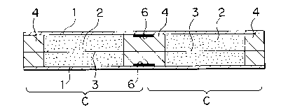
In FIG. 1, the electrical double-layer
30capacitor cell according to the first embodiment of
the present invention is shown. Reference numerals
corresponding to those of FIG. 4 are used for like
parts and numeral 6 denotes an insulating thin film.
In the present invention, a plural number (two
35in FIG. 1) of cells C are provided having common
collecting electrodes 1. However, in the case of
adhering each collecting electrode 1 to gasket 4, at
.
, .~.
2023631
approximately the central part of the surface of the
gasket 4 between adjacent cells C, i.e. other than
the gasket portions at both ends or terminals, an
insulating thin film 6 is intervened. In the part
where in the insulating thin film 6 has been
intervened, the collecting electrode 1 and the gasket
4 are caused not to adhere.
For example, in the case when adherence is
carried out by heat melting, paper, a Teflon sheet,
or a plastic sheet which is not heat melted, etc. is
used as the insulating thin film 6, and this is
previously pasted on the gasket 4, and the collecting
electrode 1 is put thereon and heat melted to the
gasket. As a result of the procedure described
above, the part where the collecting electrode 1 and
the gasket 4 have the insulating thin film 6 between
them is not heat melted.
Also, in the case when the adhesion is carried
out by use of an adhesive agent, the adhesive agent
is not coated on the insulating thin film 6 pasted on
the gasket 4. In this manner, the part of the
collecting electrode 1 overlying the insulating thin
film 6 on the gasket 4 is also not adhered to the
gasket.
Although in the above-described example, it
has been assumed that the insulating thin film 6 is
previously pasted on the gasket 4, it may also be
pasted in a corresponding position to the collecting
electrode 1.
FIG. 5 shows an exploded perspective view of
the first embodiment wherein symbols corresponding to
those of FIG. 1, are used and 4-1 denotes an open
port part or space provided in the gasket 4 in order
to be filled with a polarizing, electrode 2. At
predetermined positions on the inner surface of each
collecting electrode 1, insulating thin films 6 are
each pasted and open port part for filling use as 4-
'.~
.. ..
- 7 _ 2023631
1, is filled with a polarizing electrode 2. The
polarizing electrodes 2 may be of the paste-like, or
of the solid plate-like types.
The entire shape of the multi-cell arrangement
produced in a manner as described above is flat
plate-like and has the thickness of one cell, C and
thus is not bulky. Also respective cells C are
initially all connected in parallel by the common
collecting electrodes 1. In order to use this
embodiment as a capacitor cell arrangement having a
desired breakdown voltage and capacity, it is treated
as follows.
FIG. 6 shows a perspective view of the first
embodiment at the time of use, with symbols
corresponding to those of FIG. 1, numeral 1-1 and 1-2
denote collecting electrode pieces, 8 denotes mark
lines, and Cl to C4 are depicted on the exterior
surface in such a manner as to let the position where
the insulating thin films 6 are intervened be
discernible from outside.
In FIG. 6, the portion of the upper collecting
electrode 1 at the position where the insulating thin
film 6 has been located between cells C-3 and C-4 and
the portion of the lower collecting electrode at the
position where the insulating thin film 6 has been
located between cells C-2 and C-3 already have been
is cut out in a manner as shown in the figure. When
the collecting electrode pieces 1-1 and 1-2, which
are under intermediate way of being cut off, and the
collecting electrode piece (not shown in this figure)
of the lower collecting electrode 1 present at the
position directly below the upper collecting
electrode piece 1-1 are cut off along the mark lines
8, the cells C-l to C-4 become all in series
connection. The portions of the collecting
electrodes 1 situated between the cells play the role
~f~
. ..
- 8 - 2023631
electrodes 1 situated between the cells play the role
of a conductor for connection between the respective
cells.
If it is assumed that the collecting electrode
piece 1-1 is cut off, but the collecting electrode
piece 1-2 is not cut off, then the result is a
parallel connected body of the cells C-l and C-2
connected in series with the cell C-3.
Also, in the case when only the collecting
electrode piece 1-1 and the portion of the lower
collecting electrode present at the position directly
below the collecting electrode piece 1-1 have been
cut off, the cells C-l to C-4 become a parallel
connection.
In a manner as described above, by only
performing such a simple procedure for suitably
cutting off the collecting electrode 1 along the mark
line 8, it becomes possible to connect cells
arbitrarily in series or parallel to form a capacitor
cell arrangement having desired breakdown voltage and
capacity.
The reason why the insulating thin film 6 has
been intervened is that the adhesion of the
collecting electrode 1 to the gasket 4 is prevented
in order for the cutting off of the collecting
electrode 1 to easily be effected.
In order for the cutting off of the collecting
electrode to more easily be effected, the mark line 8
may be replaced with sewing machine, needle holes.
However, since the mark line 8 has only the object of
being the yardstick for cutting off, it is not
necessary.
SECOND EMBODIMENT
Fig. 2 shows the electrical double-layer
capacitor cell according to the second embodiment of
the present invention. Reference symbols
~
_ 9 _ . 2023631
corresponding to those of FIG. 1 are used for like
parts and numeral 7 denotes a ditch or groove.
The second embodiment can be considered as a
changed example of the first embodiment, with the
only difference being that, in place of the
intervention of the insulating thin film 6, a ditch
or groove 7 is provided in the surface of the gasket
4.
Due to the ditch 7, the collecting electrode 1
and the gasket 4 are separated for the width of the
ditch, and the adhesion of the collecting electrode 1
and the gasket 4 at this location is prevented. This
embodiment is possible in the case when the thickness
of the gasket 4 is large.
THIRD EMBODIMENT
FIG. 3 shows the electrical double-layer
capacitor cell according to the third embodiment of
the present invention. Again, reference symbols
corresponding to those of FIG. 1, are used for like
parts and numeral 5 denotes a gap or space.
This embodiment is one in which a plural
number of individual cells C are assembled by making
the collecting electrodes 1 as common electrodes or
sheets and gaps 5 are provided between such cells.
Therefore, the entire shape is flat plate-like and
has the thickness of once cell and all cells are
initially in parallel connection.
FIG. 7 shows the perspective view for
explaining the structure of the third embodiment. In
order to make the inside structure easily
understandable, there is depicted a state in which
the collecting electrode 1 on the upperside is rolled
up to an intermediate position.
There are provided cells C5, C6, etc. which
have the respective polarizing electrode Z filled in
the respective gaskets 4 which are separated by gaps
.~
. ~ j ,~ ,~
-
lO- 2023631
5. However, since the collecting electrodes 1 of all
cells are again each formed as a respective single
common sheet, all of the cells are in parallel
connection.
FIG. 8 is a perspective view of the third
embodiment at the time of use. Symbols corresponding
to those of FIGS 3 and 7 are used for like parts.
Numeral 8 denotes a cutting mark line, and C5 to C9
individual cells.
At the time of use, in order to get the
breakdown voltage and capacity corresponding to the
request, a process is carried out such that the
portion of the collecting electrode 1 at the position
of a gap 5 is suitably cut off, and the cells are
made in series connection, parallel connection, or
series parallel connection.
For example, in the case when cells C5, C6 and
C7 are desired to be provided in series connection,
(1) the portion of the upper collecting electrode
1 covering the gap 5 between the cell C5 and the cell
C6 is cut off in a manner as shown for the collecting
electrode piece 1-3,
(2) the portion of the collecting electrode
covering the gap 5 between the cells C6 and C7 is cut
off, (as already shown) and
(3) the portions of the upper and lower collecting
electrodes 1 covering the gaps behind the cells C5,
C6 and C7 are cut off (as shown for the upper
electrode).
In the third embodiment, since this embodiment
with the gaps 5 is liable to flex, the adherence of
the capacitor cell arrangement to a curved surface
and the like becomes easy.
Although the invention has been described in
its preferred form with a certain degree of
particularity, it is understood that the present
disclosure of the preferred form has been changed in
- ll - 2023631
the details of construction and the combination and
arrangement of parts may be resorted to without
departing from the spirit and the scope of the
invention as hereinafter claimed.
'~ ~
,~