Note : Les descriptions sont présentées dans la langue officielle dans laquelle elles ont été soumises.
1 2026873
MECHANICAL/ELECTRICAL DISPLACEMENT TRANSDUCER
This invention relates in general to apparatus for
sensing displacement or position of an object, and in
particular to apparatus which utilizes a flexible
moveable band or other moveable element to convert a
physical measure of displacement and position of an
object into an electrical signal representing such
measure.
In the operation of various mechanical and electro-
mechanical systems, it is necessary to monitor the
position and displacement of either some element of
the system or some object which is not part of the
system. For example, in robotic systems (a technology
whose use is dramatically increasing) it is almost
always necessary to monitor and control the movement
and position of various component parts of the
systems, such as an arm, fingers or other grasping
elements, etc. Such monitoring and control yields
the dexterity and precision required for a robotic
system to carry out its functions.
Prior art mechanisms for sensing position and
displacement have most often utilized a direct
connection between the article or object whose
position or displacement was to be monitored, and
some type of gauge, needle or other visual indicator.
-- 2026873
Movement of the article or object would thus cause a
corresponding movement of the gauge or needle. As
expected, such mechanisms have typically been large
and cumbersome and have lacked precision in carrying
out the monitoring function. Further, since some type
of sliding action of some part of the measuring
mechanism typically was involved, friction was
present which, of course, resulted in wear.
Although electronic apparatus for measuring position
and displacement has come into greater use in recent
years and has at least partially solved the bulkiness
and imprecision problems of the prior art mechanisms,
such apparatus has been complicated in design and, as
a result of such complication, generally lacking in
reliability. Also, the contact friction and attendant
wear generally remained.
It is an object of the invention to provide a simple,
efficient and reliable apparatus for measuring
position and movement of a component or article.
It is another object of the invention to provide such
apparatus which is compact and contains few moving
parts.
It is a further object of the invention to provide
such apparatus which avoids the need for sliding,
friction-producing components.
It is also an object of the invention to provide such
apparatus which is well-suited for use with
semiconductors and integrated circuits.
It is still another object of the invention to
provide such apparatus which can be fabricated
utilizing conventional integrated circuit fabrication
- 2026873
technology for at least part of the apparatus.
The above and other ob~ects of the invention are
realized in one speclflc lllustratlve embodlment of
displacement measuring apparatus adapted for measuring
posltlon and movement of an ob~ect. The dlsplacement
measurlng apparatus lncludes a sensor (or plurallty of
sensors), formed wlth at least one surface area, for produclng
an electrlcal output slgnal whose value varles wlth varlation
ln the proxlmlty of a band element to the surface area, and an
elongate, flexlble band dlsposed ln proxlmlty wlth the surface
area so that at least a portion of the band is caused to
selectlvely roll over and cover or unroll from over and
uncover at least a portion of the surface area when the ob~ect
is moved. Movement and positlon of the ob~ect, whlch causes
the band to roll over or unroll from over the surface area of
the sensor, ls thus determlned by the electrlcal slgnal
produced by the sensor (or sensors).
In accordance wlth the lnventlon there ls provlded
dlsplacement measurlng apparatus comprlslng an element whose
dlsplacement is to be measured, sensor means including a
substrate havlng a flrst surface area, an elongate, flexlble,
electrlcally conductlve band havlng a flrst end and a second
end, sald flrst end of the band belng coupled to sald element
to move when sald element ls moved, and sald second end of the
band belng jolned to the flrst surface area so that at least a
portlon of the band overlles the flrst surface area, the
amount of such portion varylng as the flrst end of sald band
h
69912-164
2026873
3a
is moved, and sald sensor means further lncludlng means, at
least a portion of whlch is dlsposed at the flrst surface, for
detectlng the portlon of the band overlylng the flrst surface
area and thus the dlsplacement of sald element, whereln said
detectlng means comprises a field-effect transistor having a
source region, at least one draln reglon, and a channel reglon
positioned between the source region and drain reglon.
In accordance with one aspect of the lnventlon, some
portlon of the band ls fixed relatlve to the sensor and some
other portlon ls coupled to the ob~ect. Movement of the
ob~ect toward or away from the surface area of the sensor, or
generally parallel therewlth, wlll cause the band to change
lts locatlon relatlve to the surface area and thls change ls
detected by the sensor.
In accordance wlth another aspect of the lnventlon,
a voltage ls supplled to the band to cause lt to produce an
electrlc fleld and the sensor ls comprlsed of a fleld-effect
translstor for detectlng the magnltude of the electrlc fleld
produced by the band and thus the proxlmlty of the band to the
fleld-effect translstor. Alternatlvely, the band may be
69912-164
2026873
magnetized and the sensor may comprise a split-drain
magnetic field-effect transistor for detecting the
strength of the magnetic field developed by the band
and thus the position of the band relative to the
magnetic field-effect transistor. Other sensor
configurations, for example utilizing the Hall effect,
capacitive sensing, optical sensing and sonar sensing,
may also be employed to detect the movement and
location of the bands to thus detect the movement and
location of the object. In addition, the sensor area
of sensitivity may be constructed to allow for
producing a signal whose value varies in a
predetermined (linear or nonlinear) way with movement
of the band.
In accordance with still another aspect of the
invention, a displacement measuring device utilizes a
magnetized or electrically charged rotatable or
linearly moveable element coupled to the object whose
position is to be measured, and an array of magnetic
field or electric field detectors to detect the
position of the element and thus of the object.
In the drawings:
The above and other objects, features and advantages
of the invention will become apparent from a
consideration of the following detailed description
presented in connection with the accompanying drawings
in which:
FIGS. lA, lB and lC are perspective, side
elevational and fragmented end perspective
views respectively of displacement measuring
apparatus utilizing a field-effect transistor
in accordance with the principles of the
present invention;
5 2026873
FIG. 2 is a fragmented end perspective view of
displacement measuring apparatus utilizing
capacitive coupling in accordance with the
present invention;
FIG. 3 is a perspective view of displacement
measuring apparatus utilizing a split-drain
magnetic field-effect transistor in accordance
with the present invention;
FIG. 4 is a perspective view of displacement
measuring apparatus utilizing an electret sheet
and a field-effect transistor in accordance
with the present invention;
FIG. 5 is a perspective view of displacement
measuring apparatus utilizing the Hall effect
in accordance with the present invention;
FIG. 6 is a side, elevational view of
displacement measuring apparatus utilizing
capacitance variation to detect movement of an
object in accordance with the present
invention;
FIG. 7 is a side, elevational view of
displacement measuring apparatus utilizing a
continuous band for measuring two degrees of
freedom movement of an object in accordance
with the present invention;
FIG. 8 is a perspective view of displacement
measuring apparatus utilizing two continuous
bands for measuring movement of a joystick in
accordance with the present invention;
6 2026873
FIGS. 9A and 9B show respectively an isometric
view and side, elevational view of rotational
displacement measuring apparatus made in
accordance with the present invention;
FIGS. lOA and 10B show respectively a
perspective view and a side, elevational view
of an alternative embodiment of a continuous
rotational displacement measuring apparatus
made in accordance with the present invention;
FIG. 11 is a side, elevational view of
apparatus for measuring rotational displacement
of a cylinder in accordance with the present
invention;
FIG. 12 is a side, elevational view of another
embodiment of apparatus for measuring
rotational displacement of a cylinder in
accordance with the present invention;
FIG. 13 is a side, elevational view of
displacement measuring apparatus for measuring
two degrees of freedom of linear movement of an
object and another degree of freedom of
rotational movement of the object, in
accordance with the present invention;
FIG. 14 is a perspective view of displacement
measuring apparatus for producing a digital
output representing the position and movement
of an object, in accordance with the present
invention;
FIG. 15 is a perspective view of displacement
apparatus for producing discrete output
increments in response to movement of an
7 2026873
object, in accordance with the present
invention;
FIG. 16 is a perspective view of displacement
measuring apparatus for producing a nonlinear
output in response to movement of an object, in
accordance with the present invention;
FIG. 17 is a perspective view of displacement
measuring apparatus utilizing a linearly
moveable, wedge-shaped element;
FIG. 18 is a perspective view of another
rotational displacement measuring apparatus
made in accordance with the present invention;
FIG. 19 is a perspective view of still another
rotational displacement measuring apparatus
made in accordance with the present invention;0
FIG. 20 is a perspective view of displacement
measuring apparatus utilizing optical sensing
in accordance with the present invention;
FIG. 21 is a perspective view of another
embodiment of displacement measuring apparatus
utilizing optical sensing;
FIG. 22 is a side elevational view of still
another displacement measuring apparatus
utilizing optical sensing;
FIG. 23 is a side, elevational view of
- displacement measuring apparatus utilizing
acoustic sensing;
FIG. 24 is a graphic view of displacement
2026873
measuring apparatus of the present invention
utilized for weighing;
FIG. 25 is a side, elevational view of
displacement measuring apparatus of the present
invention utilized for temperature measurement;
FIG. 26 is a side, elevational view of
displacement measuring apparatus of the present
invention used for measuring the angle between
two elements pivotally joined together at their
ends;
FIG. 27 is a side, elevational view of
displacement measuring apparatus of the present
invention utilized also for weighing;
FIG. 28 is a side, elevational view of
displacement measuring apparatus of the present
invention utilized for measuring acceleration;
FIG. 29 is a side, elevational view of
displacement measuring apparatus of the present
invention utilized for measuring velocity;
FIG. 30 is a perspective view of displacement
measuring apparatus utilizing electrical
resistance variation to detect movement of an
object in accordance with the present
invention;
FIG. 31 is a perspective view of another
embodiment of displacement measuring apparatus
utilizing electrical resistance variation to
detect movement of an object; and
F~G. 32 is a side, elevational view of
2026873
displacement measuring apparatus of the present
invention utilized for measuring, among other
things, acceleration and other force producing
phenomena.
Referring now to the drawings:
Referring to FIGS. lA, lB and lC, there is shown one
illustrative embodiment of a band-controlled
transducer or sensor for measuring two degrees of
freedom of movement of an object 4. The object 4
(which is simply in the form of a plate in FIGS. lA
through lC) may take any shape or form and could be a
part of a robotic system, or other mechanical
structure for which the part's position and movement
is to be determined. The object 4 is attached to one
end of an elongate, flexible, electrically conductive
band 8. The other end of the band 8 is affixed, by a
suitable adhesive, pin or other fastening means, to
one end of a substrate 12 made, for example, of
silicon and having an upper generally planar surface
in which are disposed the operating parts of a sensor
for sensing the position of the band 8. The
band 8 is coupled to a voltage source 16 to enable it
to produce an electric field.
Disposed on and formed, for example, by conventional
microfabrication techniques on the upper surface of
the substrate 12 is a field-effect transistor (FET)
20. The FET 20 is a well-known semiconductor device
and includes a conductive source region 24 formed in
the substrate 12, a conductive drain region 28 spaced
from and formed to be generally parallel with the
source region, and a conductive channel region 32
disposed between the source region and drain region.
A layer of insulation 36 is disposed over the upper
surface of the substrate 12 and over the source,
2026873
drain and channel regions 24, 28 and 32.
The source region 24 and drain region 28 are
maintained at different electric potentials by a
vol~age source 34 so that electric current is caused
to flow between the regions through the channel 32.
The conductivity o the channel region 32 is affected
by electrical charges (or an electric field) located
in close proximity to the channel region. Thus
rolling and unrolling the band 8 over the insulation
layer 36 to selectively cover and uncover the FET 20
will vary the magnitude of the electrical current
being conducted through the channel region 32 and
detected by a meter (ammeter) 38. The band 8
e~fectively acts as the gate of the FET 20 to control
the flow of electrical current between the source
region 24 and the drain region 28. Measuring this
current flow can thus provide a measure of the rolling
and unrolling of the band ~ and thus a measure of the
position and movement of the object 4. A further
discussion oE the operation of F~TS is found in U.S.
Patent No. 4,767,973, issued August 20, 1988.
The band 8 might be constructed of any suitably
flexible, electrically conductive material such as
copper ~oil, aluminum foil, metalized polymer film,
metalized quartz, metalized thin silicon, etc.
Advantageously, the band 8 is formed so that its
lateral edges curve downward slightly toward the
substrate 12 (when overlaying the substrate) so that
the band will roll over and unroll from the insulation
layer 12 in a consistent, nonsliding fashion to
maintain contact with the insulation layer.
Electrostatic attraction can also be used to hold the
band 8 snugly against the insulation layer 12.
11 2026873
The band 8 and substrate 12, with component parts,
may all be fabricated using microfabrication
techniques. The band 8, for example, could be sputter
deposited over the substrate 12 and then
photolithographically etched to define the desired
size and shape. An etchant could also be used to
release a portion of the band from the substrate and
allow it to cure away from the substrate.
An alternative to utilizing a conductive band 8
connected to a voltage source 16 is to provide a band
of material containing positive or negative charges.
For example, the band 8 could illustratively be formed
from flexible polytetrafluoroethylene with electrons
implanted therein.
Another alternative to the FIGS. lA through lC
embodiment would be to include a layer of conductive
material between the layer of insulation 36 and the
substrate 12 and then position the FET 20 remotely
from the band 8 contact region. This conductive
layer or gate would be electrically coupled to the
gate of the remote FET so that rolling the band 8 over
the insulation layer 36 would induce an electrical
charge on the surface of the conductive layer located
under the insulation strip 36 and this electrical
charge would be reflected in the gate of the remote
FET to affect the conductivity of the channel region
of the FET. A measure could then be made of the
proximity of the band 8 over the insulation layer 36
and thus of the position and movement of the object 4.
FIG. 2 shows an alternative embodiment of a band-
controlled displacement measuring device which
utilizes capacitive coupling in conjunction with an
FET. In this embodiment, a substrate 40 carries the
source, channel and drain regions of an FET 44 at the
12 2026873
upper surface and near one side of the substrate
(similar to the FIG. lA through lC embodiment) and a
conductive strip of material 48, arranged generally in
parallel with the source, drain and channel regions of
the FET 44, near the other side of the substrate.
Coupled to the conductive strip 48 is an AC electrical
voltage source 52. A dielectric layer of material 56
is disposed on the upper surface of the substrate 40
and over the FET 44 and conductive strip 48. A
flexible, electrically isolated, conductive band 60 is
then disposed to roll over and unroll from over the
dielectric layer 56 as an object or component to which
the band is coupled is caused to move.
The signal supplied by the voltage source 52 to the
conductive strip 48 develops a capacitance between the
conductive strip and the band 60 and this capacitance,
of course, results in the development of a charge on
the band and this charge affects the conductivity of
the channel region of the FET 44. AS the band 60 is
rolled over and unrolled from the dielectric layer 56,
the capacitance is caused to change, changing the
affect on the FET 44 and the conductivity of the
channel region thereof. AS with the FIGS. lA through
lC embodiment, the change in conductivity of the
channel region can be monitored as a determination of
the movement and position of the band 60 and thus of
an object or component coupled to the band.
FIG. 3 shows a perspective view of displacement
measuring apparatus utilizing a split-drain magnetic
field-effect transistor (MAGFET) 64. The MAGFET 64 is
formed on the upper surface of a substrate 68 and
includes a source region 72 coupled to a D.C. current
source 76, two drain regions 80 and 84, and a
conductive channel region 88 disposed between the
source region and the two drain regions. A flexible,
2026873
13
magnetizable band 92 is disposed on the substrate 68
to selectively cover and uncover the channel region
88. A layer of insulation 96 could, but need not
necessarily, be disposed over the MAGFET 64 and under
the band 92.
In the absence of a magnetic field impinging upon the
channel region 88, current flows from the source
region 72 through the channel region 88 equally to the
two drain regions 80 and 84. When a magnetic field is
present, such as when the magnetized band 92 is at
least partially overlying the channel region 88, the
current through the channel region is deflected to
flow more to one drain region than the other, with the
magnitude of the deflection and thus the imbalance of
current flowing to the two drain regions being
dependent upon the intensity of the magnetic field.
This intensity, of course, will depend on what portion
of the channel region 88 is covered by the band 92 and
so by measuring the current imbalance in the two drain
regions 80 and 84, a measure of the displacement of
the band and thus of an object to which the band is
coupled can be made. The band 92 might illustratively
be made of a thin film of alnico alloy (aluminum,
nickel, cobalt and sometimes copper), alloy of nickel
and cobalt, samarium cobalt, ferric oxide, ferric
chromium, chromium dioxide, etc., appropriately
magnetized.
30 FIG. 4 is a perspective view of displacement
measuring apparatus which utilizes an electret sheet
of material lOO in which are implanted or disposed
electrons. The electret sheet 100 is positioned over
and attached to a substrate 104 in which is formed an
35 FET 112 in a fashion similar to that described for
FIGS. lA through lC. Positioned to move over and
cover and move from over and uncover the electret
` 14 2026873
sheet 100 is a flexible conductive band 108. The band
108 is attached at one end to the electret sheet 100
and is coupled to a ground potential 116. The other
end of the band 108 is joined to an object or element
whose position is to be measured.
The device of FIG. 4 operates using a ~capacitive
divider" effect in which the electric field produced
by the electret sheet 100 is directed uniformly
outwardly from the sheet when the band 108 is not in
close proximity, and is directed towards the band
when the band is in close proximity. Thus, the
electric field of the electret sheet 100 will be
directed towards the FET 112 to affect the
conductivity of the channel region thereof when the
band 108 is curled away from the sheet, and will be
redirected away from the FET 112 and towards the band
108 when the band is in position over the sheet. Thus
the conductivity of the channel region of the FET 112
20 is determined by the proportion of the electret sheet
112 covered by the band 108. In a manner already
described, the device of FIG. 4 could thus be used to
measure movement and position of an object.
The electret sheet 100 might illustratively be made of
polytetrafluoroethylene, charged with electrons.
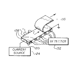
FIG. 5 is a perspective view of another embodiment of
displacement measuring apparatus where the well-
known Hall effect is utilized. The apparatus includesa substrate of conductive material 120, such as copper
alloys, aluminum alloys, etc. A current source 124
supplies current to one end of the substrate 120 to
flow therethrough to the other end. A series of pairs
of electrodes 128 are positioned on opposite sides
along the length of the substrate 120 and are coupled
to a detector 132. A magnetized, flexible band 136 is
2026873
attached at one end to one end of the substrate 120 to
selectively roll over and unroll from over the
substrate as earlier described.
In accordance with the Hall effect, current flowing
in a conductor is deflected from one side of the
conductor towards the other side when the conductor is
subjected to a magnetic field. Thus in the FIG. 5
device, when the magnetized band 136 is overlying a
portion of the substrate 120, the current flowing from
one end of the substrate to the other is deflected at
that portion but is not deflected at the portion which
is not overlaid by the band. This current deflection,
in the form of a voltage drop, is detected by the
detector 132 to provide a measure of that portion of
the substrate 120 which is covered by the band 136 and
thus a measure of the movement of an object or
component to which the free end of the band 136 is
coupled.
FIG. 6 is another embodiment of a displacement
sensing device made in accordance with the present
invention. This device includes a pair of conductive
plates 140 and 144 spaced apart a distance D and
coupled to a voltage source and detector 148. Two
dielectric layers 152 and 156 are disposed on the
facing surfaces of plate 140 and 144 respectively as
indicated. A pair of elongate, flexible and
conductive bands 160 and 164 are each joined at one
end to a side of a respective dielectric layer 152
and 156 to extend forwardly along the respective layer
and then inwardly and rearwardly where th~ other ends
of the bands are joined together, as shown in FIG. 6.
The other ends of the bands 160 and 164 are coupled to
an object 168 whose position and movement is to be
detected. As the object moves toward a position
between the plates 140 and 144, more of the bands 160
2026873
- 16
and 164 are caused to roll over and overlay dielectric
layers 152 and 156 respectively. Of course, as the
object 168 moves in a direction away from between the
plates 140 and 144, the bands 160 and 164 are unrolled
from covering respective dielectric layers. Movement
of the object 168 and thus movement of the bands 160
and 164 causes a variation in the capacitance between
the plates 140 and 144 which variation is measured by
the A.C. voltage source and detector 148, which for
example could include an ammeter. The effective
configuration of the capacitor plates is graphically
illustrated at 172 for the situation where the bands
160 and 164 have been unrolled from between the plates
140 and 144. The effective capacitor configuration
for the situation when the bands 160 and 164 are
rolled between the plates 140 and 144 is illustrated
at 176. The graphic representations 172 and 176 show
the effective difference in capacitance for when the
bands 160 and 164 are between the plates 140 and 144
versus when the bands are not between the plates.
Thus, variation in the capacitance between the plates
140 and 144 provides a measure of the movement and
position of the object 168 as desired.
An alternative capacitive measuring device to FIG. 6
involves the use of only one band, for example band
160, and provision of only one conducting plate, for
example plate 144, with the other plate, for example
plate 140, being nonconductive. Then, the voltage
source and detector 148 would still be connected to
plate 144, and also band 160 to develop a capacitance
between the plate 144 and band 160. This capacitance
would vary as the band 160 was rolled over or unrolled
from over the nonconductive plate 140, caused by
movement of the object 168, to thereby provide a
measure of the position and movement of the object.
17 2026873
FIG. 7 is a side, elevational view of displacement
apparatus utilizing a continuous band to measure two
degrees of freedom of movement of an object 180. The
apparatus includes a substrate 184 having two FET
sensors 188 and 192 linearly spaced apart in the
upper surface of the substrate. An insulation layer
196 is positioned on the substrate 184 over the FET
sensors 188 and 192. A flexible conductive band 200
is formed into a loop and disposed on the insulation
layer 196 to roll back and forth over a locus on
which the FET sensors 188 and 192 are disposed.
When the object 180 is moved to the right in FIG. 7,
the band 200 is caused to also roll to the right to
cover FET sensor 192 and to uncover FET sensor 188.
This movement, of course, is detectable by the sensors
to provide an indication of both the direction of
movement of the object 180 and the magnitude of the
movement. If the object 180 is moved upwardly, the
band 200 is caused to unroll from both sensors 188 and
192 and this also is detectable. Movement of the
object 180 to the left or downwardly can be detected
in a similar fashion so that movement to the right or
left, and up or down of the object 180 can be readily
detected. The band 200, of course, would carry an
appropriate charge so as to produce an electric field
either from a voltage source or from charges embedded
in the band.
Although the FIG. 7 device was described as utilizing
FET sensors, it should be understood that other type
sensors described earlier could also be utilized such
as MAGFETs, capacitive coupling, electret sheets, and
Hall effect sensing.
FIG. 8 is a perspective view of displacement
measuring apparatus for measuring the position and
2026873
18
movement of a joystick 204. The apparatus includes a
substrate 208 on the surface of which are located four
FET sensors 212, 216, 220 and 224, positioned along
intersecting imaginary lines as shown. An insulation
layer 228 is disposed on the substrate 208 over the
four sensors. Disposed on the substrate 208 are two
flexible, electrically conductive bands 232 and 236
both formed into loops and disposed crosswise of one
another. The joystick 204 is pivotally affixed in the
substrate 208 to extend upwardly through openings in
the bands 232 and 236, including openings 240 formed
in band 236 and opening 244 formed in band 232. To
allow movement of the joystick 204 without bending
either of the bands 232 and 236 sideways, the openings
240 and 244 are formed crosswise in the respective
bands and crosswise with respect to one another as
shown in FIG. 8. Thus, the joystick 204 may be moved
toward sensor 216 or sensor 224 to thereby move the
band 232 without bending the band 236 sideways.
Similarly, the joystick may be moved towards sensor
212 or sensor 220 to move band 236 without bending
band 232 sideways. Such movement of the joystick 204
and thus of the bands 232 and 236 is detected by the
particular sensors affected when the sensors are
covered or uncovered as described for earlier
embodiments.
Again, the bands 232 and 236 would be charged to
produce electric fields as described for earlier
embodiments. Also, the bands 232 and 236 might
advantageously be secured at lower sections to the
substrate 208. Finally, other sensing arrangements
described earlier could also be used with the FIG. 8
device.
FIGS. 9A and 9B show respectively an isometric view
and a side elevational view of apparatus for measuring
19 2026873
rotational displacement of a shaft 250. The shaft 250
is mounted to rotate in substrate 254 in which is
disposed in an annular configuration an FET sensor 258
having conventional source, drain and channel
regions. An insulation layer 262 is positioned on the
substrate 254 over the FET sensor 258. A disk 266 is
mounted on the shaft 250 above the substrate 254 to
rotate as the shaft is rotated. A flexible,
electrically conductive band 270 is attached at one
end to the insulation layer 262 and at the other end
to the bottom of the disk 266 so that when the shaft
250 is rotated in one direction (for example,
clockwise looking down on the device), the band is
caused to lay down over the sensor 258, and when
rotated in the opposite direction, the band is pulled
up from over the sensor. Rotational movement and
position of the shaft 250 can thus be detected by the
sensor 258.
The displacement measuring apparatus shown in FIGS.
lOA and lOB utilize a continuously formed band 280
folded over itself to contact both the upper surface
of an insulation layer 284 disposed over a substrate
288, and the underneath surface of a disk 292 mounted
to rotate with a shaft 296. The shaft 296 is mounted
to rotate in the substrate 288. An FET sensor 300 is
formed generally in a circle as best seen in FIG. lOA
so that as the shaft 296 and thus the disk 292 are
rotated, that portion of the band 280 which is in
contact with the disk 292 is carried with the disk so
that the lower portion of the band progressively
covers and uncovers different portions of the sensor
300. The band 280 might illustratively be affixed to
the lower surface of the disk 292 although with
appropriately fabricated bands, the holding of the
band 280 to the underneath surface of the disk could
be accomplished by electrostatic attraction, surface-
tension with a thin film of liquid, magnetization,
20 2026873
etc. When the band 280 is not attached either to the
disk 292 or the insulation layer 284, it is self-
aligning in the radial direction, i.e., it will
automatically space itself uniformly about the shaft
296. The device of FIGS. 10A and 10B, of course,
provides for measuring angular position and movement
of the shaft 296 as the band 280 is caused to cover
and uncover different portions of the sensor 300.
Other types of sensors as discussed above could also
be utilized in lieu of the FET sensor 300, and in lieu
of the FET sensor 258 of FIG. 9A.
FIGS. 11 and 12 show embodiments of apparatus for
measuring the angular movement and displacement of
cylinders 304 and 324 respectively. The cylinder 304
in FIG. 11 includes conductive plates 306 and 308
formed or attached to the exterior of the cylinder. A
hollow cylinder 310 is disposed about the exterior of
rotatable cylinder 304, but is spaced therefrom in
fixed position. A pair of plates 312 and 314 are
carried on the inside surface of the hollow cylinder
310 and spaced apart as shown. Plates 306, 308, 312
and 314 all include a dielectric layer of material on
their exposed facing surfaces. Two flexible,
electrically conductive bands 316 and 318, formed into
loops, are disposed between the cylinder 304 and the
cylinder 310 to roll over the interior surface of the
cylinder 310 and the exterior surface of the cylinder
304 as the cylinder 304 is rotated about a fixed axis
320. In a manner similar to that described for the
FIG. 6 apparatus, the capacitance developed between
plates 306 and 314 and plates 308 and 312 varies as
the bands 318 and 316 respectively move between or out
from between the respective plates so that measuring
the capacitance provides a measure of the rotational
displacement and movement of the cylinder 304.
- 2026873
21
Other sensor configurations could also be used in the
FIG. 11 structure including FETs, MAGFETs, electret
sheets, etc.
In the FIG. 12 embodiment, as the cylinder 324 is
rotated about a fixed axis 325, it causes a band 326
formed into a loop to roll back and forth on the
surface of a substrate 328 in which is disposed in a
linearly spaced-apart relationship two FET sensors
330 and 332. The position of the band 326, detected
by the sensors 330 and 332, thus provide an indication
of the rotational position of the cylinder 324.
FIG. 13 is a side, elevational view of displacement
measuring apparatus for measuring two linear degrees
of freedom of movement of a plate 350 and one degree
of freedom of rotational movement of the plate. The
apparatus includes a substrate 354 in which are
formed on the upper surface thereof two linearly
spaced-apart sensors 356 and 358. The plate 350
likewise includes at its lower surface two linearly
spaced-apart sensors 360 and 362. A flexible,
electrically conductive band 364 formed into a loop is
positioned between the plate 350 and substrate 354 to
roll back and forth laterally and selectively cover
and uncover the sensors 356, 358, 362 and 360 which
accordingly produce electrical outputs representing
the amount of coverage by the band. ThiS, of course,
provides a reading or measure of the location and
movement of the plate 350. The sensors 356, 358, 360
and 362 could take a variety of forms as earlier
discussed.
FIG. 14 is a perspective view of displacement
measuring app~ratus for producing a digital output
signal representing position of a flexible band 370
and thus of an object 374 to which the band is
22 2026873
attached. A substrate 378 includes a plurality of
sensors 382 positioned at selected intersections of an
imaginary grid on the surface of the substrate so that
as the band 370 is rolled over the substrate,
different combinations of sensors are affected and
these combinations produce binary coded output
signals. For example, if only sensor 382 were covered
by the band 370, then that sensor would produce an
output signal which would represent the numeral 8. If
the band 370 were moved to also cover sensors 382b,
then they would produce output signals representing
the numeral 7, etc. In this fashion, digital output
signals are produced to represent different positions
of the band 370 over the substrate 378 and thus
different positions of the object 374.
FIG. 15 shows a perspective view of apparatus for
also producing discrete output increments representing
the movement or position of a flexible band 390 and
thus of an object 394. Positioned on a substrate 398
are a plurality of drain regions 402 interleaved with
a plurality of source regions 406. The drain regions
402 are connected to a common conductor 410 and the
source regions 406 are also connected to a common
conductor 414. Disposed between each adjacent drain
region and source region are channel regions 418 to
effectively define a plurality of FETs arranged in a
linear array on the substrate 398. As successive
channel regions 418 are covered or uncovered by the
band 390, the current flow on conductors 410 and 414
changes to thus provide an indication of the position
of the band 390 and thus of the object 394.
In FIG. 16 is a perspective view of apparatus for
producing a nonlinear output in response to movement
of a band 420. Disposed on a substrate 424 is a
field-effect transistor having a drain region 428, a
2026873 -
23
source region 432 and a channel region 436 disposed
therebetween. The channel region 436 varies in width,
being widest at the opposite end of the substrate 424
from where the band 420 is attached and gradually
tapering inwardly as it runs toward the end of the
substrate to which the band is attached. The drain
region 428 and source region 432 extend generally
parallel with respective sides of the channel region
436 as shown in FIG. 16. When the band 420 is moved
to cover the substrate 424, increasingly wider
sections of the channel region 436 are covered by the
band and so the current change with movement of the
band is nonlinear. Of course, the channel region 436
could be formed to taper in the opposite direction to
provide a different nonlinear output with movement in
the band; various other shapes for the channel region
could also be selected to produce nonlinear outputs.
FIG. 17 shows an embodiment of displacement measuring
apparatus which does not utilize a flexible band.
Rather, a wedge-shaped, electrically energized plate
430 is employed. The plate 430 is suspended above a
substrate 434 (for example, by being attached to an
object whose position is to be measured) to move
forward or backward in a crosswise direction of the
substrate as an object to which the plate would be
attached is moved. The plate 430 is coupled to a
voltage source 438 to be energized thereby. The
substrate 434 includes an FET with a source region
442, channel region 446 and drain region 450. So
long as the plate 430 was maintained out of contact
with the substrate 434, no insulation layer would be
required, although as a precaution it would probably
be advisable to include it as an overlay of the
substrate.
As can be seen from FIG. 17, as the plate 430 is
2026873
24
moved in the direction of the peak of the plate
(forwardly), a larger area of the plate covers the
channel region 446 of the FET and this, of course,
causes a change in conduction between the source
region and drain region. As the plate 430 is moved in
the opposite direction (rearwardly), less of the plate
430 covers the channel region 446 so that again a
change in conduction between the source and drain
region occurs. This change in conduction is
detectable to determine the position of the plate 430
and thus of the object to which it is connected.
FIGS. 18 and 19 are perspective views of other
embodiments of rotational displacement measuring
apparatus made in accordance with the present
invention, but not utilizing flexible bands. The
apparatus of FIG. 18 shows an axle or shaft 460 which
would be attached to an object whose angular position
and displacement was to be measured. The shaft 460 is
mounted to rotate about its long axis in a substrate
464. Mounted to extend laterally from the shaft 460
to rotate therewith is an arm 468 having a wedge-
shaped cross-section with the apex of the wedge
developing a line-charge effect directed downwardly
toward the substrate 464. The arm 468 is coupled to a
voltage source 472 to receive an electrical charge
therefrom. Alternatively, the arm 468 could carry an
electrostatic charge for example as a result of
electrons being embedded in the arm. Disposed
generally in a circle under the path of movement of
the arm 468 are a plurality of FET sensors 476.
As the shaft 460 is rotated (because of movement of
the object to which it is connected), the arm 468 is
caused to sweep over different ones of the sensors 476
which detect the electric field emanating from the arm
to t~ereby generate a signal indicating the position
2026873
of the arm. Obviously, that sensor 476 producing the
strongest signal would be the sensor over which the
arm 468 is positioned.
Although the sensors 476 are shown with some spacing
therebetween on a substrate 464, the sensors could
have a variety of sizes and spacing, with more sensors
providing for greater sensitivity in determining
angular position of the shaft 460.
FIG. 19 also is adapted for measuring angular
displacement of a shaft 480 which is mounted to rotate
about its long axis in a substrate 484. Mounted to
rotate with the shaft 480 is a semicircular plate 488
to which an electrical charge is supplied by a voltage
source 492. The plate 488, like the arm 468, rotates
above the top surface of the substrate 484. Formed in
the upper surface of the substrate 484 are four FET
sensors 496, 500, 504 and 508. Each of the FET
sensors is formed in a semicircle (with parallel
extending source, drain and channel regions) to be
concentric with at least a portion of two of the other
sensors. Thus, sensor 496 circumscribes a portion of
sensor 500 and a portion of sensor 508 while sensor
504 circumscribes the other parts of sensor 500 and
508. As the plate 488 is rotated, it will always
cover portions of at least three of the FET sensors,
and in most positions it will cover portions of all
four of the sensors.
3~
In operation, the FET sensors 496, 500, 504 and 508
produce signals indicative of the proportion of the
sensor affected by the electric field produced by the
plate 488 and thus by the portion of the sensor which
is covered by the plate. The signals, in turn, define
the angular position of the shaft 480 and thus the
angular position of the object to which the shaft is
26 2026873
connected.
FIGS. 20, 21 and 22 all show band-controlled
transducers which utilize optical sensing. In FIG.
20, a light source 520 directs light downwardly
towards a substrate 524 over the top surface of which
an opaque band 528 is disposed to roll and unroll as
an object to which the band is connected is moved.
Formed in the top surface of the substrate 524 is an
elongate photocell 532 which produces an output signal
supplied to a detector 536 whose magnitude is
proportional to the amount of light impinging on the
photocell. As the band 528 rolls to cover and unrolls
to uncover the photocell 532, the amount of light
blocked by the band, and thus the amount of light
impinging upon the photocell 532 varies to thereby
cause a variation in the output signal from the
photocell. This output signal thus provides a measure
of the position of the band 528 over the photocell and
thus a measure of the position of the object to which
the band is connected.
FIG. 21 shows an alternative embodiment of a
displacement measuring device utilizing optical
sensing. Here, a substrate 540 includes a plurality
of light-emitting diodes 544 formed in the upper
surface of the substrate and energized by a current
source 548. A flexible, opaque band 552 is attached
at one end to one end of the upper surface of the
substrate 540 to roll and unroll over the light-
emitting diodes 544 as an object to which the band is
coupled is moved. Light from the light-emitting
diodes 544 is projected upwardly, unless blocked by
the band 552, to be detected by a photocell 556. As
with the FIG. 20 embodiment, the photocell 556
produces an output signal whose magnitude is
proportional to the amount of light impinging thereon
-
27 2026873
and this output signal is detected by a detector 560.
Thus, as the band 552 is caused to roll over and
unroll from over the substrate 540 and the light-
emitting diodes 544, varying amounts of light are
allowed to reach the photocell 556 to thereby vary the
magnitude of the output signal of the photocell. This
output signal thus provides an indication of the
position of the band 552 over the substrate 554 and
thus a measure of the position of the object to which
the band is connected.
FIG. 22 shows a side, elevational view of another
embodiment of displacement measuring apparatus
utilizing optical sensing. Here, a substrate 570
includes a plurality of photocells 574 disposed on the
upper surface thereof. A flexible, light-reflective
band 78 is attached at one end to one end of the upper
surface of the substrate 570 to roll and unroll from
over the upper surface thereof as an object 582, to
which the band is attached, is caused to move. A
light source 586, for example a laser light source,
directs a beam of light 588 toward the band 578 at a
location which will reflect the light beamed
downwardly towards the upper surface of the substrate
570. The light beam will thus be caused to impinge
upon one of the photocells 574 depending upon the
position of the band 578 and thus depending upon the
position of the object 582. The photocell upon which
the light beam is impinging, of course, produces an
output signal indicating receipt of the light and such
signal is indicative of the position of the band 578
and object 582.
It should be understood that whenever photocells in
the embodiments of FIGS. 20 and 21 were shown as being
a single photocell, that a series of individual
photocells could also be utilized. Also, a series of
2026873
28
light-emitting diodes 544 are shown in FIG. 21, but a
continuous strip of light could also be utilized.
FIG. 23 is a side, elevational view of a band-
controlled transducer which utilizes acoustic sensing.
Here, a band 590 is connected at one end to a
substrate 592 and at the other end to an object 594
whose position and movement is to be measured.
Disposed generally at one end of the substrate 592 in
the direction in which the band 590 would roll down
over the substrate is a sonar signal source 596 for
transmitting acoustic signals toward the band 590, and
an acoustic detector 598 for detecting signals
reflected back from the band. The detector 598
detects the time of travel of the acoustic signals
which, of course, varies depending upon the position
of the band 590 and thus the position of the object
594. Of course, there is no need for any substrate
based detecting elements since the detection of the
position of the band 590 is accomplished by the
acoustic signal source 596 and detector 598.
FIGS. 24, 25, 26, 27, 28 and 29 all show specific
applications of the use of the band-controlled
transducers described earlier. FIG. 24 is a graphic
view of displacement measuring apparatus of the
present invention utilized for weighing. Here, a
spring 600 interconnects a moveable element 604 to a
fixed support 608. A holding plate 612 for holding an
object 616 to be weighed is coupled by connecting
lines 620 to the moveable element 604. A substrate
624 includes a sensor formed in the surface 628 over
which a flexible band 632 is disposed to roll and
unroll, as discussed in the earlier embodiments. One
end of the band 632 is attached to the lower end of
the substrate 624 and the other end of the band is
attached to the moveable element 604 to allow the
--- 2026873
29
desired rolling and unrolling of the band. The
substrate 624 with sensor 628 is coupled to a display
device 636 to provide a reading representing the
magnitude of the output signal of the sensor and thus
a reading of the weight of the object 616.
FIG. 25 is a side, elevational view of temperature
measuring apparatus. A substrate 650 includes a
sensor 654 formed in the upper surface thereof. A
flexible band 658 having a first thermal expansion
coefficient is attached at one end to one end of the
substrate 650 to overlay a portion of the substrate.
A second band 662 having a second thermal expansion
coefficient overlays the first-mentioned band 658. A
voltage source 666 is coupled to the band 658 to
supply a charge thereto.
As the ambient temperature to which the device of
FIG. 25 is subjected changes, the bands 658 and 662
are caused to expand at different rates causing the
curling or uncurling of the two bands from the surface
of the substrate 650. For example, if the thermal
expansion coefficient of band 658 is greater than that
of band 662, then as the temperature rises, the two
bands will tend to curl away from the substrate 650.
Of course, as the band 658 rolls over or unrolls from
over the sensor 654, the output signals from the
sensor vary to indicate the position of the band 658
and thus the ambient temperature.
FIG. 26 shows a device for measuring the angular
position between two elongate elements 680 and 684.
The elements 680 and 684 are joined at one end to
pivot about a pivot point 688. Linear sensors 690 and
694 are attached to elongate elements 680 and 684
respectively and a flexible, electrically or
magnetically energized band 698 is attached at its two
202687~
ends to elements 680 and 684 so that the band extends
inwardly, overlaying a portion of the sensors 690 and
694 in a bow shape. As the elements 680 and 684 are
pivoted closer together, more of the band 698 overlays
the sensors 690 and 694 and as the elements are
pivoted away from one another, less of the band
overlays the sensors. The sensors 690 and 694 detect
the proximity of the band 698 to produce signals
indicating the relative positions of the elements 680
and 684, as discussed for the previous embodiments.
FIG. 27 shows an alternative weighing device
including a substrate 704 having a sensor 708 formed
in the upper surface thereof. A platform 712 is
mounted on springs 716 and 720 to maintain a position
generally in parallel with and above the substrate
704. A flexible band 724 is connected at one end to
one end of the substrate 704 and at the other end to
one end of the platform 712. When an object 728 is
placed on the platform 712 to be weighed, the platform
is caused to move downwardly closer to the substrate
704 to thus cause the band 724 to roll over and cover
more of the sensor 708. The weight of the object 728
determines the extent to which the band 724 covers the
sensor 708 and this is detected by the sensor to
provide a readout in a readout device 732 of the
weight of the object.
FIG. 28 is a side, elevational view of an
accelerometer including a substrate 750 having a
sensor 754 formed in the upper surface thereof. A
band 758 is attached as previously described to the
substrate 750 and is attached at the free end to a
mass 762. The mass, in turn, is coupled by a spring
766 to a rigid support member 770 which is mounted on
the substrate 750. As the device of FIG. 28 is
accelerated to the right or left, the mass 762 is
31 2026873
caused to move to the left or right respectively
depending upon the magnitude of the acceleration (and
stiffness of the spring 766) and this movement, in
turn, causes the band 758 to roll over or unroll from
over the sensor 754 which detects the movement. In
this manner, acceleration of the device of FIG. 28
can be measured. The spring 766 restores the mass 762
to a rest position when no acceleration is taking
place.
Finally, FIG. 29 shows a side, elevational view of
apparatus for measuring velocity of an object 780.
When the object 780 is caused to move left or right at
a certain velocity, a band 784 to which the object is
attached is caused to roll over or unroll from over a
substrate 786 at one-half the velocity of movement of
the object. The band is made of a conductive material
and is coupled via a resistor 788 and ammeter 790 to a
DC current source 792. The other side of the current
source 792 is coupled to a conductive plate 794 which
is disposed on top of the substrate 786. A dielectric
layer 796 overlays the conductive plate 794 and is
positioned under the band 784. The current source 792
produces a capacitance between the plate 794 and that
portion of the band 784 which is overlying the
dielectric layer 796. As the object 780 is caused to
move at a certain velocity to the left or right in
FIG. 29, the band 784 either covers or uncovers the
dielectric layer 796 at one-half that velocity causing
a change in the capacitance between the band and the
plate 794. This change, which is proportional to the
velocity of the object 780, causes a current to flow
through the resistor 788 and this current is detected
by the ammeter 790 to provide a measure of the
velocity of the object 780. Other arrangements for
measuring current produced as a result of a change in
capacitance could also be provided as discussed
2026873
earlier .
FIGS. 30 and 31 show perspective views of
displacement measuring apparatus utilizing electrical
resistance variation to detect position movement of an
object attached to the end of a flexible band. In
FIG. 30, the band 800 is attached at one end to roll
and unroll from over a substrate 804. The free end of
the band would be attached to the object (not shown)
whose movement was to be detected. Formed in the
upper surface of the substrate 804 are two resistive
strips of material 808 and 812 which extend generally
parallel with one another in a spaced-apart
relationship lengthwise on the substrate. The
resistive strip 808 is coupled to a current source 816
and the resistive strip 812 is coupled to an ammeter
820 and then to the current source 816. The band 800
is made of a conductive material so that current flows
from the current source 816 through that portion of
the resistive strip 808 not in contact with the band,
through the band to the resistive strip 812 and then
through the ammeter 820 back to the current source.
The greater the length of the resistive strips 808 and
812 through which current must flow, the lower is the
current because the resistance of the flow path is
greater, and vice versa. Thus, as the band 800 is
caused to roll over or unroll from over the resistive
strips 808 and 812, the resistance in the flow path is
caused to change, resulting in a variation in the
current flowing through the ammeter 820 and this
variation is measured to thereby provide a measure of
the position of the free end of the band 800. The
resistive strips might illustratively be made of
nickel-chromium deposited on polymer strips (for
example mylar) attached to the upper surface of the
substrate 804.
2026873
33
FIG. 31 also measures the position of the free end of
the band 830 utilizing electrical resistance
variation. Here, the band 830 is attached at one end
to a substrate 834 on the upper surface of which are
disposed two conductive strips (for example, metal)
838 and 842 arranged to be generally parallel with one
another as shown. Conductive strip 838 is coupled to
a current source 846 and conductive strip 842 is
coupled through an ammeter 850 to the other side of
the current source. The band 830 is made of a
flexible, resistive material to conduct current
between the conductive strips 838 and 842 but to
present a predetermined resistivity. A current path
is established in the FIG. 31 apparatus from the
current source 846 through the conductive strip 838
and across that portion of the band 830 in contact
with the two conductive strips to the conductive strip
842 and then through the ammeter 850 back to the
current source. As the free end of the band 830 is
caused to move, the band rolls over and unrolls from
over the conductive strips 838 and 842 to vary the
total resistance of the current flow path between the
two strips and, as this resistance varies, the current
through the ammeter 850 is also caused to vary to
thereby provide a measure of the position of the free
end of the band 830. The resistive band 830 could
illustratively be made of nickel-chromium deposited on
a thin polymer sheet of material, of graphite filled
rubber, etc.
As described, the FIGS. 30 and 31 apparatus both
measure position and displacement of an object
connected to a flexible band by utilizing electrical
resistance variation in a current flow path.
FIG. 32 shows a side, elevational view of a type of
null-band sensor apparatus in which an elongate mass
2026873
34
or strip 860 bridges between and is attached to two
conductive band loops 864 and 868. The band loop 864
is positioned to bridge between two conductive plates
872 and 876 disposed on a substrate 874. The plates
872 and 876 are connected respectively to voltage
sources 878 and 880. The magnitude of the voltage
signal supplied by the voltage sources 878 and 880 to
respective plates 872 and 876 is controlled by a
servologic circuit 884 which receives inputs from
sensors 886 and 888 formed in a linear spaced-apart
position on the upper surface of substrate 890. m e
sensors 886 and 888 could be of the types previously
described.
In operation, when the mass 860 is caused to move to
the left or right in FIG. 32, for example, by a force
applied thereto, by acceleration of the FIG. 32
device, etc., the bands 864 and 868 are caused to roll
over the respective substrates on which they are
disposed and the movement of band 868 is sensed by the
sensors 886 and 888 which signal the servologic
circuit 884 accordingly. The servologic circuit 884,
in response to the signals from the sensors, signals
the voltage sources 878 and 880 to produce an
electrostatic attraction in a corresponding one of the
plates 872 and 876 to attract the conductive band loop
864 and cause it to roll back towards a rest or null
position. Thus, if the mass 860 had moved to the
left, the plate 876 would be energized to attract the
band 864 and cause it to roll back to the null
position midway between plates 872 and 876, and vice
versa. In the manner described, a null-position
acceleration (or other force) sensor is provided.
It is to be understood that the above-described
35 arrangements are only-illustrative of the application
of the principles of the present invention. Numerous
modifications and alternative arrangements may be
2026873
devised by those skilled in the art without departing
from the spirit and scope of the present invention and
the appended claims are intended to cover such
modifications and arrangements.