Note : Les descriptions sont présentées dans la langue officielle dans laquelle elles ont été soumises.
~2~ 3
This invention is a wireless electrical
resistance chip, adapted in such a way as to be soldered
eventually on a printed circuit card or an hybrid circuit
substratum. Such a resistance is part of a new family of
new components for electronics, generally known under the
specific term of surface mounting components.
This inv0ntion is also concerned with the
fabrication of this electrical resistance.
We know how to manufacture resistance chips in
such a way as to form a resisting element or resistive
layer applied on an electrically insulated substratum in
a square or rectangular shape of a few square
millimeters.
The laying of this resisting element is
realized by silkscreen printing with pastes or resisting
inks layed directly on this substratum. The thickness of
the layer applied is in the order of several micrometers
and its electrical resistance varies between few ohms and
several megaohms. This technique is known by people in
the field under the specific term of deposit in thick
layers. We also know how to manufacture the same type of
components by layering by vacuum depositing technique of
resisting materials notably of the chromium-nickel type
or Constantan directly on the said substratum. Under
these conditions, the ohmic value of the component so
realized may vary b~tween few ohms and few tens of kilo-
ohms, the thickness of the layer varying typically
between 10 and few thousand nanometers. This technique
is known under the specific term of vacuum depositing.
The extremity electrodes of these known resistances are
made according to techniques of layering by thick layers,
notably by deposit of Ag-Pd alloys on the substratum,
done in such a way as to form an electrical continuum
with the resisting material and by rechargin~ later by
electrolytic techniques the said Ag-Pd alloy with thick
nickel, Sn and Pd-Sn layers.
The fabrication of these resistances in chips
according to the depositing in thick or thin layers is
realized by forming the resisting layer on a large
insulatin~ substratum, in the order of few tens of square
centimeters and by dividing later the substratum by
sections in comb or strip shapes. The resisting ele~ent
or resistance layer is protected by a protective layer of
organic matter of the photoresist type. The extremity
electrodes are formed on the top of the component and the
whole is treated at high temperature in order to give to
the said electrodes an as weak as possible conductibility
as well as a good mechanical hold.
Each of the sections in strip shape is then cut
in units of a few square millimeters and finally an
electrolytic deposit of Ni and Pb-Sn or equivalent is
applied on each chip. This way, we obtain a resistance
in the form of a surface mounted chip.
This process is described for example in the
D~-A-3 148 778, the US-A-~ 27~ 706, the EP-A-0 lgl 538
and the US-A-4 792 781.
The resistances manufactured by these known
processes present however the disadvantage, by their
nature, not to be precise and to have characteristical
temperature and response variations in frequency
prejudicial to the performances e~pected today for
electronic circuits.
Indeed, the tolerances in ohmic value of these
resistances are seldom lower than few per cent of the
nominal value of the resistance. Also, their temperature
coefficient, represented by the variation of the nominal
resistance a~cording to the temperature is never lower
than 100 to 200 parts per millions/ degree Celsius
(ppm/~C).
Moreover, the variations of the nominal
resistance with time, can be between few thousands and
serveral thousands parts per million (ppm).
The object of the present invention is to
compensate for these inconveniences by making a
resistance chip for surface mounting with an ohmic value
tolerance in relation to the nominal value in the order
of 0,1% to 0,05%.
Another object for this present invention is to
realize a resistance chip ~ith a temperature coefficient
inferior to 5 ppm/~C.
Another ob~ect of the present invention is to
realize a resistance chip with a nominal variation of
resistance in time limited between 50 and 200 ppm for a
duration of between ~000 and 10,000 hours at 155~C.
Another object of this present invention is to
realize a resistance chip having all the advantages
described above, while keeping the properties of
soldering and reliability generally associated with very
high precision components.
Another object of the present invention is to
provide a method permitting to manufacture a resistance
chip which presents the above defined characteristics.
The invention thus concerns an electrical
resistance chip, intended to be soldered notably on a
printed circuit card or on an hybrid circuit substratum
of the electrically insulating ceramic type, on which is
2~ joined by an adhesive layer of organic resin, a shset of
metal or a resisting alloy, such a sheet being cut-out by
engraving to form filaments connected together to
constitute a meandering resisting circuit. This cut-out
resisting shee~ is covered by another layer of organic
resin.
According to the invention, this resistance is
characteri2ed in that the aforementioned other layer of
resin leaves free on both opposite sides of the
substratum two extremities of the cut-out resisting
sheet, in that these two parts of the resisting sheet are
each covered by a thin layer of a metal or a'lloy stickin~
to the resisting sheet, this layer being covered by a
second thicker layer of metal or conducting alloy ; and
this second layer being also covered by a third thicker
layer of a soldering alloy, these three superimposed
layers are equally spread out on both opposite lateral
sides of the substratum and partially on the face of the
substratum which is opposite to the cut-out resisting
sheet.
The three successive metallic layers covering
the two extremities of the resisting sheet, as well as
the lateral opposite sides of the substratum and part of
the face of the substratum opposite to the one holding
the resisting sheet, permit to establish an electrical
connection between the resisting element (the engraved
sheet) and notably an hybrid or printed circuit.
The invention allows thus to realize a chip
form of resistance being surface mounted, and having a
resisting element a metallic sheet being engraved instead
of a resisting layer obtained following the technique of
thick or thin layers.
The tests performed by the applicants have
shown that such a resistance presented at least the
following characteristics
- temperature coefficient inferior to 10 ppm
per ~C,
- ~hmic value tolerance inferior to 0,~1 %,
- variation of this value with time inferior to
1000 ppm at 155~C and 10,000 hours.
According to a preferred version of this
invention, the said extremity parts of the resisting cut-
out sheet do not spread up to the two lateral opposite
sides of the substratum but leave free two of the
opposite zones adjacent to the said lateral faces of the
substratum in such a way that the three metallic layers
successively recover on each side of the resistance, a
part of the cut-out resisting sheet, then a section of
5 2 ~ 4 ~
the substratum not covered by the said re~isting sheet
and bare of resin, then, successively -the lateral side of
the substratum and part of the surface of the substratum
opposite to that which bears the resisting sheet.
The tests done by the applicants have shown
that in this case, the resistance presented the following
performances:
- temperature coefficient below 5 ppm per ~C,
- Ohmic value tolerance below 0,005%,
- variation of this value in time below 500 ppm
at 155~C and for l0,000 hours.
According to another aspect of the invention in
the manufacturing method of the electrical resistance, on
the substratum is glued a resisting metallic sheet with a
resin, the said resisting sheet is engraved (or etched)
in order to form a sinuous contoured resisting filament
presenting extremity parts intended ~or the electrical
connections of the resistance, we apply on the said
engraved sheet, a second layer of resin, such a process
being characterized by the following steps:
- removing by engraving the said second layer
of resin on the said extremity parts of the engraved
sheet fot the electrical connections,
- applying on the said extremity parts of the
2~ engraved sheet not covered by the resin, a metallic
coating spread on each of the lateral sides of the
substratum and in part on the side of the substratum
opposite to the side holding the engraved shee-t, this
metallic coatin~ being formed by the following successive
layers, a thin layer of chromium or titanium-tungsten
alloy, a thicker layer of a nickel-chromium alloy, then a
layer of nickel or gold.
Other particularities and advantages of the
invention will appear in the following description:
To the anne~ed drawings given as examples, but
not to be limited to them:
~2~
6 ..
- figure 1 is a perspective view of -the sheet
glued on its subs-tratum, and constituting the first step
of the process as given in the invention,
- figure 2 is a perspective view of the
resistance a~ter engraving of the sheet,
- figure 3 is a cross-sectional view of the
resistance after protection of the sheet by an engraved
layer of resin,
- figure 4 is a view in perspective
illustrating the fourth step of the manufacturing
process: preferential engraving of the gluing resin layer
of the sheet, along the edges of the said resistance,
- ~igure 5 is a cross-sectional view
illustrating the fifth and sixth steps of the
: 15 manufacturing process: the application of the thin layer
of Ni-Cr or Cr by vacuum application and application of
the Nickel layer by electrolytic process,
: - figure 6 is a view in perspective showing the
final appearance of the resistance chip,
- figure 7 is a cross-sectional view of an
alternative realization o~ a resistance according to the
invention.
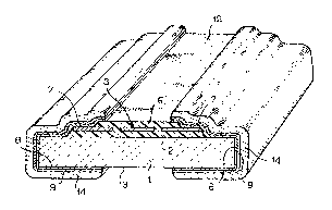
The resistance chip according to the invention
: is formed by the following elements (see also figures 6
and 7):
1. An insulating substratum 1 of a ceramic
type, preferably but not restricted to aluminum oxyde,
0.2 to 0.6 mm thick and measuring 2 to 3 mm in surface,
precisin~ that these dimensions are not restrictive and
may vary in large proportions depending upon the
constraints imposed by the electrical power ~issipated by
the resistance or all other constraints, size or
mechanical in connection with the characteristics of the
circuits using these resistances.
2. An adhesive layer 2 o~ the resin epoxy type
or other matter presenting good adhesive properties as
7 ~2~
well as good mechanical and electrical hold under the
thermic, chemical and mechanical constraints laid upon
the said ceramic substratum, and designed to affix
permanently a sheet of metal or resistive alloy 3 on the
substratum 1.
3. A resistive metal sheet 3 constituted of Ni-
Cr alloy or other matter presenting the same
characteristics of resistance as Ni-Cr, 2 to 10
micrometers thick, glued on the ceramic substratum 1 and
engraved through a photoresistant mask in the shape of
conducting filaments, presenting a continuous Greek
design fret, controlled in width and length with extreme
precision. The resistive metal sheet 3 is then protected
by a layer 6 of resin (epo~y or analogous) of the same
nature as the gluing layer 2 between the ceramic 1 and
the sheet 3. This technology of fabrication, designed
notably to make electrical resistances, has been
described in the American patents 3 ~105 589 and 3 517 436
; ZANDMA~, as well as in the French patents 2 344 940 and
2 354 61~ of the applicant. This process produces
extremely stable and precise electrical resistances.
4. A thin and extremely adhesive layer 8 of
metal or of chromium or nickel-chromium alloy, deposited
around the edges of the substratum 1 and in intimate
electrical and mechanical contact with the resistive
metal sheet 3 glued on the substratum 1.
5. A thick sheet of metal or conductive alloy
such as Nickel 9, covering the thin film ~ in order to
render electrical contact as conductive as possible and
permitting a good metallic base for later soldering.
6. A thick layer 1~ of soldering alloy of the
tin-lead type covering the whole of the layers of nickel
or chromium or of nickel-chromium, permitting to solder
on printed or hybrid circuits the resistance ~Inder the
best of conditions.
2 ~
We will first describe in references to figures
1 to 6 the manufacturing process of the preferred version
of a resistance chip in accordance with the invention.
First step (figure 1), a resin 2 ~for example
epoxy or polyimide or any other type of glue which can
tolerate the mechanical and thermic constraints), is used
to glue a sheet 3 of nickel and chromium alloy of a
thickness varying between 2 and 10 micrometers, on an
insulating substratum 1 ~for exemple, made of ceramic of
the aluminum oxyde, beryllium oxyde, or aluminum nitrate
or anyother ceramic whith good dielectrical properties at
all temperatures as well as excellent hardness and
mechanical strength properties) of a thickness varyiny
between 0.2 and 0.6 mm and a surface of 0.5 to a few
square millimeters.
In a second step, using the traditional means
of photolithography and well kno~n in the micro-
electronic industry, the sheet 3 is applied on a
photoresistant mask, bearing openings showing a
resistance pattern similar to those described in the
patents mentioned above.
In a third step, the whole is brought to a
chemical, electrochemical or ionic machining, as
described for example in the American patents 3 517 436
and 3 905 389 (ZANDMAN) in the French Patents 2 344 940
an~ 2 354 ~17 o~ the applican~, in order to engrave the
parts of the resistive sheet 3 not protected by the
photoresistor.
After removal of the photoresistor, the whole
substratum 1 and sheet 2 look like the sketch presented
on figure 2, in which the reference 4 represents
schematically the resistance as an engraved filament
folded in a greek shape fret with, at its extremities
shaped during the same process of photoengraving, the
exit segments 5, designed to connect the resistance on
the outside, the entire sec~ion closely adherin~ to the
g
substratum 1 by the layer of resin 2. The engraving mas~
has been designed so that the lateral dimension _ of the
resistive element 3, 4 and 5 is sensibly smaller than the
width D of the substratum 1 and is between 0.8 D and 0.6
D. Thus, there remain on each side of the extremity
parts 5 of the engraved sheet 3 some free areas.
In a fourth step, represented by figure 3, the
active part of the resistance 3 is protected by a thick
protective layer of resin 6 preferably of identical
nature to layer 2, or of a polyimide type in order to
bring a long lasting protection against humidity and
corrosion.
The lateral dimension of this protectiorl area
is sensibly smaller than d, in order to leave free as
much as possi~le of the contact areas 5. This resin
layer 6 is applied by silkscreen printing or other
process.
In a fifth step, a thick layer (in the order of
5 to 10 micrometers) of photoresist is used to protect
the parts 6 and 5, so that it also leaves exposed the
lateral sides 7 of the resistance, recovered by the layer
of the gluing resinO
The section of the layer of resin 2, not
protected by the photoresist is then removed by etching.
Qne of the preferred means of the invention, is to submit
the whole o~ the resistance to a plasma formed by a
mixture of oxygen and gaseous fluorized compounds of the
carb~n fluoride type. The engraving speed of the plasma
being sensibly equal for the photoresistant and for the
resin 2, the result of this process, presented by figure
4, is to leave bare and perfectly free of any trace of
resin, the adjacent sections on both opposite sides of
the substratum 1.
The si~th step of the process, presented in
drawing 5, is to apply by vacuum process a thin layer 8
of contact on the exit areas 5 of the resistive sheet 3
,,,
as well as on the lateral sides 7 of the substratum 1.
One of the preferred methods of the invention is to
deposit by cathodic pulverization, on the said areas and
surfaces 5 and 7, first a chromium layer ~, of a
thickness of between 10 and 50 nanometers, followed by a
deposit of 9, a nickel-chromium alloy, at an atomic
concentra~ion of chromium varying between 20% and 50%,
and a thickness between 500 and 1500 nanometers. The
purpose of the deposit 8 is to form between the sheet 3
and the layer 9, an interface liable to give an excellent
ohmic contact combined with good adhesive strength
between the sheet 3 and the layer 9. A third layer of
nickel or gold 14 is then applied. One of the preferred
means of the invention is to use, to achieve the said
deposit, the electrolytic techniques appropriate for
metal and alloy applications. Another method preferred
by the invention is to apply instead of the chromium
layer 8, an alloy of the titanium-tungsten t~pe, which
allows a better mechanical pull with the sheet 3 than
pure chromium. This layer covers also parts 7 all the
while assuring a smooth transition between the exit areas
5 and the parts 7. This permits a maximum reduction of
the mechanical and thermic constraints which may develop
at the level of the areas 5 due to a dilatation
coefficient difference between 1, 2 and 3. This
optimiza~ion permits to guarantee that the value of the
resistance chip will be practically constant in time and
under te~perature variations during its use. This
phenomenon is further increased by the utilization of the
cathodic pulverization method, which has the property of
increasing the adhesive properties of thin layers
deposited on the exit parts 5 and the substratum 1.
Before the deposition process, metallic masks
10 and 11 have been placed by appropriate mechanical
3~ means on the faces 12 and 13 of the resistance in order
to protect them of all traces of chromium, nickel-
. .
chromium and of nickel or gold~ The application is done
to cover with a uniform layer all of the surfaces of the
sheet 2 and of the substratum 1, protected or not
protected by the metallic mask 10 and 11. After the
vacuum-depositing and electrolytic processes, the
metallic masks 10 and 11 are removed. This process
removes mechanically the thin layers which became
deposited on these masks. The result of this process is
shown on figure 6. The layers of plating 8, 9 and 14
then form a stretched C shaped ohmic contact,
electrically connecting the resistance to sheet 3 via the
e~it areas 5 to the lower surface 13 of the substratum.
When the connecting process with the remainder
of the hybrid or printed circuit is realized by micro-
soldering using a gold or aluminum wire, the material
forming the layer 14 is achieved by electrolytic gold
plating.
When the chip resistance is intended to be
soldered on the said printed circuit or the said hybrid
circuit by tin~lead soldering, then, the layer 14 is made
by electrolytic nickel plating. It is then covered by
appropriate means of dipping in a tin-lead bath, of a
tin-lead layer 5 to 20 micro~eters thick.
In the realization shown on figure 7, parts 5a
of the engraved resistive sheet 3 are spread out
practically to opposite lateral edges of the substratum
lo This way, contrary to the realization shown on figure
6, there are no free segments between the edge of parts
5a and the adjacent edge of the substratum.
However, as in the realization shown on figure
7, parts 5a of the engraved resistive sheet 3 are covered
by three metallic layers 8, 9, 14 identical to those
shown on figure 6, which spread to the lateral sides of
the substratum as well as on part of the face 13 of the
substratum opposite to the side bearing the engraved
resistive sheet 3.
12
As in the preferred realization and according
to figure 6, these khree metallic layers form a
con~uctive coating in cross-section in the shape of a C,
covering the entire length of compound on its two
5 opposite sides.
The chip resistance thus obtainad presents also
performances superior to those resistances realized by
the techniques of layer thick or thin, due to the great
precision with which the resistive element 3 can be
obtained in the form of a cut-out or engraved sheet.
However, the performances (~emperature
coefficient, ohmic value and variation tolerance) are
inferior to those of a resistance of the one shown on
figure 6).
The superiority of the resistance represented
on figure 6 is essentially explained by the presence of
free sections 7 included between the edges of the parts 5
of the resistive sheet 3 and the adjacent edges of the
substratum 1 which allow as explained above, to reduce
the thermic and mechanical constraints on the parts 5 of
the engraved resistive sheet 3 due to the dilatation
coefficient differences between the substratum 1, the
resi layer 2 and the resistive layer 3.
Of course, the invention is not limited to the
manufacturing examples just described and we may bring to
these numerous modifications without leaving the
parameters of the invention.