Note : Les descriptions sont présentées dans la langue officielle dans laquelle elles ont été soumises.
- 2029038
SPECIFICATION
..
Title of the Invention
PROCESS AND SYSTEM FOR PREPARING
SA SUPERCONDUCI ING THIN FILM OF OXIDE
J
. Background of the blvention
pjç~d of the invention
The present invention relates to a process for preparing a
l 0superconducting thin film of oxide, more particularly, to an improved
process for depositing a thin film of superconducting compound oxide on
a substrate by Molecular Beam Epitaxy (hereinafter, MBE) technique.
The present invention relates also to a system for carrying out the
~! process automatically ~y a computer.
~- Descri~tion of the related art
,
Thin films of compounds are prepared by so-called reaction-
evaporation method in which materials are evaporated in an active gas
atmosphere so that vapors of the materials are reacted with the acthe gas
20 on a substrate to deposit a thin film of the compound on d~e substrate.
Whèn the compound is an oxide, oxygen is usual1y used as the active gas.
In Tatsumi et al. "Epitaxial film growth of artificial (Bi-O)/(Sr-Ca-Cu-O)
layered structure", Appl. Phys, Lett. 54 (23) June 5, 1989 p. 2364-2366,
~- ~ an oxide supercondùcting thin film of Bi-Sr-Ca-Cu-O system is grown
25 epitaxially by ion-beam sputtering technique in the presence of oxygen
gas. It is also proposed to use exited oxygen which is activated by
microwave in order to obtain an oxidc thin film of high quality.
~ .
' '1'
.,
.,.~ . .
'' J~
2029038
Thin films of compounds composed of more than two elements are
advantageously prepared by the MBE technique in which proportions of
constituent elements of the compound can be controlled precisely. A
combination of the MBE and dle reaction-evaporation is much effective
S for some compounds. D. G. Schlom et al. "Molecular beam epitaxy of
layered Dy-Ba-Cu-O compounds", Appl. Phys. Lett. 53 (17) Oct. 24,
1988, p 1660-1662 disclose a modified MBE process in which a thin film
of oxide superconductor of Dy-Ba-Cu-O is prepared with introducing
excited oxygen gas which is activated by microwave.
10In a high-temperature superconductor possessing a layered
perovskite crystalline structure composed of constituent layers each
containing different elements, the constituent layers are stratified
successively on a substrate. Superconductive property of a final product
is influenced critically by the content of oxygen atoms in constituent
15 layers. Therefore, it is extremely important to control supply of oxygen
gas to each constituent layer. ~ fact, it is diffilcult to obtain a desired
, clystal structu~e of high-temperature oxide superconductor by the Icnown
modified MBE process in which constituent layers are deposited
continuously widlout controlling dle oxygen supply, so that the quality of
2 û the final product obtained by the known modified MBE is rather poor.
An object of the present invention is to solve the problem and to
provide an improved MBE process for preparing thin films of oxide
superconductors of high quality and a system for carrying out the process
automatically by a computer.
:!
.` 1~ 1 .
~ '......... ' '
.', ~ ' , : ' '' '
- 2029038
Summarv of the ~vention
The present invention provides a process for preparing a ~in film
of oxide superconductor having a layered c~ystal structure by depositing
constituent layers of said layered crystal structure on a substrate by
S Molecular Beam Epitaxy (MBE) method while an oxygen-containing gas
which is exited by irradiation of microwave is introduced in the
neighborhood of a surface of the substrate, characterized in that, after
predetermined numbers of constituent layers which correspond to one
unit crystal or less than one unit crystal are layered, a fflm-forming
10 operation by the MBE method is interrupted temporally and the deposited
constituent layers are maintained in an activated oxygen atmosphere in
ôrder to effect a crystallization promotive operation and then next film-
forming operation by the MBE method is restarted after completion of
said crystallization promotive operation, a combination of the film-
15 forming operation and the crystallization promotion operation beingrepeated for desired times until a desired ~llm thickness is obtained.
In the process according to the present invention, relative
displacement of atoms in the crystal is promoted or accelerated in a stage
of the crystallization promotion operation and satisfactorv amount of
20 oxygen is supplied to deposited layers, so that freshly deposited
constituent layers are rearranged to a desired crystal structure which is
indispensable to realizes a perfect superconductor. The thin fillm of the
final product obtained by the process according to the present invention
shows a very smooth surface of high quality whose crystallinity is
2 5 improved. This advantage is difficulty obtained by the known process in
which constituent layers are deposited continuously without interposing
~l the clystallization promotive operation according to the present invention.
-3-
'~?
., .
, ' .. ...
~,;: , '
, . . .
,` ' .
20290~8
Numbers of constituent layers after deposition of which the ~llm-
forming operation by the MBE method should be interrupted temporally
depend on kinds of oxides to be deposited. Generally, the c~ystaJlization
promodon operation can be effected after numbers of constituent layers
S which correspond tO one unit crystal are layered. When the crystal
structure of an oxide to be deposited has such many constituent layers that
are difficult to be controlled, the crystallization promotion operation may
be effected af~r numbers of constituent layers which correspond to less
than one unit crystal, for example a half of unit crystal, are layered.
The crystallization promotive operation can be carried out by
maintaining the deposited constituent layers in an oxygen-containing
atmosphere. Termination of this c~ystallization promotive operation can
, be detected by monitoring an output signal or a pattern of a ~llm analyzer
~, such as a reflection high energy electron diffraction (RHEED) analyzer
15 which is used commonly in MBE machines. In fact, high-temperature
o~ide superconductors show specfflc modulated output patterns which are
i~eP~nt to respective oxides in the RHEED analyzer, in other words, the
quality of deposited thin films can be evaluated by the RHEED pattern.
Therefore, the crystallization promotive operation can be terminated
20 when a predetermined or desired output signal of the analyzer is
observed. For example, in a case of YlBa2Cu3O7 z whose crystal has a
longer lattice constant along b-axis than along a-axis, the quality of its thin
film can be evaluated by measuring spaces of streaks in the RHEED
pattern. An o~ide superconductor of Bi4Sr4Ca4Cu6O16+~ shows a unique
2 S modulated R}EED pattern which can be used to deterrnine termination of
the crystallizadon promotive operation.
-4-
. . .
,v
.
' , ~ ` , ,
-, : ' '
.
2029038
The process according to the present invention is applicable to any
oxide superconductor which has a layered crystal structure as following:
-'. (1) (La l xax)2CuO4y
x in which a stands for Sr or Ba, "x" and "y" are numbers each
S satisfying respective range of O S x < 1 and O c y < 1,
(2) La 1 Ba 2 Cu 3 O ?-z
in which "Ln" stands for at least one element selected from the
group comprising La, Ce, Pr, Nd, Sm, Eu, Gd, Tb, Dy, Ho, Y, Er,
'r Tm, Yb and Lu and "z" is a number satisfying a range of O _ z < 1,
and
(3) Bi4(srl-kcak)mcunop+~
~: in which "k", "m", "n", "p" and "o" are numbers each satisfying
respective range of O < k < l, 6 5 m 5 lO, 4 S n < 8, p - 6+m+n
rl and-2<~_+2.
l S In ~is oxide, following proportions are preferable:
0.4ck<0.6, 75m 9, S n~7and-2C~+2,
0.2ck<0.4, 6Sm57, 4_nSSand-2C~5+2,and
O.Sck<0.7, 95m510, 7Sn58and-2S~5+2.
This oxide can be represented by the following general formula:
2 0 Bi 2 (Sr l-k Ca k) m/2 Cu n/2 (p+8)l2
because one unit crystal of the oxide is composed of two structures
of this formula which are stratif1ed symmetrically.
(4) Bi2-qpbqsr2car-lcuro~
in which "q", "r" and "~" are numbers each satisfying respective
rangeofO.l<q51, 15r56 and6~<16.
It is apparent ~at the process according to the present invention is
applicable also to the other high-temperature oxide superconductors
. - s -
... .
,~ .
'............ , ~ .
,;. ~ . . .
. . . . .
.
2029038
:
having a layered crystal structure such as Tl-containing oxide
2 superconductors, no-copper containing oxide superconductors or the ~ike.
The substrate used in the process according to the p~esent invention
has preferably the same or similar lattice constant as the oxide to be
deposited and is preferably selected from single crystals of o~ides such as
MgO, SrTiO3, YSZ, LaGaO3, LaGaO3 and LaA103. In a special case, a
single crystal of silicon may be used. If desired, a buffer layer is
interposed between the substrate and the thin film of superconducting
oxide in order to prevent mutual migration of elements and/or to
10 compensate mismatch in lattice constant. The thin film of
superconducting oxide is preferably deposited on a predetermined plane
- of the substrate. In the case of single crystal oxide substrate of MgO and
SrTiO3, a ~100) plane or a 1110} plane is preferably used. The substrate
.
is preferably heated during the operations of the process according to the
~, 15 invention at a temperature between 550 an 750 C.
- .
The oxygen-containing gas is preferably pure oxygen gas which is
exited by irradiation of microwave. This exited oxygen gas is supplied
from straight nozzle(s) or ring nozzle(s) which is positioned in the
neighborhood of a surface of the substrate where the nozzle doesn't
2 0 intersect the beams of evaporated elements. A flow rate of exited oxygen
gas depends on kinds of oxides to be deposited and/or capacity of
evacuation pumps and can be determined by experiments. The flow rate
of exited oxygen gas is usually selected between 0.1 and 50 SCCM.
The process according to the present invention can be carried out in
2 S a known modified MBE machine comprising a chamber in which a high
; vacuum can be created, means for introducing oxygen gas into the
chamber, a microwave generator for exiting the oxygen gas, means for
:.`
6-
. .
,
,`,. . ~ : : .
:, . , `:
... ..
2029~38
heating the substrate positioned in the chamber, means for controlling
independently temperatures of evaporation sources, means for controlling
independently shutters for evaporation sources, and an analyzer for
~; monito~ng crystal structures of thin films deposited on the substrate such
S as RHEED.
The process according to the present invention is preferably
autornated by using a computer, preferably a micro processor, connected
to the known MBE machine. Therefore, the present invention provides a
; system for depositing a thin film of oxide superconductor having a
- 10 layered crystal structure on a substrate by the above-mentioned molecular
beam epitaxy (MBE) machine.
The system according to the present invention is characterized in
that the clystallization promotive operation is controlled by a computer in
such a manner that, during the crystallization promotive operation, output
15 image signals from the analyzer for monitoring crystal structures of a
thin film deposited on the substrate is compared with image data of a
known superconducting oxide stored in a memory of the computer and
that next film-forming operation is restarted after the output image
signals from the analyzer ~ecome substandally identical with the image
2 0 data stored in dle memory.
The analyzer can be a reflection high-energy electron diffraction
(RHEED) analyzer and the image data of known superconducting oxide
stored in the memory of computer which is utilized in the crystallization
promotive operation can be a modulated pattern of dle RHEED ~nalyzer
2 5 which is inherent to the superconducting oxide. In practice, the output
image signals from the RHEED analyzer are converted to digital image
data in an image processor and the digital image data are compared wi~
7-
.,
. ..
"
. -.
.. . .. ..
s ~; ~
~' ,' ` ~ '
: .
2029~38
image data of known crystal structures of a superconducting oxide stored
in a memory in the computer.
It is also possible to modify operational factors such as partial
pressure of oxygen in the chamber and substrate temperature, if
S necessary, during the crystallization promothe operation.
In a preferred system according to the present invention, both of
the film-forming operation as well as the crystallization promotive
operation are automated by the computer. In this case, all operational
factors including partial pressure of oxygen in the chamber, power of the
-10 microwave generator, substrate temperature, temperatures and shuttering
order of evaporation sources during the film-folming operation are input
,,~j
,i previously in the computer and the following sequence is programed in
,.;;
. the computer:
(1) a film-forming operation in the MBE machine is interrupted
l S temporally after predetermined numbers of constituent layers which
^~ colTespond to one unit crystal or less than one unit crystal are layered,
(2) output image signals from the analyzer is compared wi~ image data
of a known superconducting oxide stored in a memory of the computer,
so that deposited constituent layers are left in an activated oxygen
2 0 atmosphere,
(3) next film-folming operation is not restarted until the output image
signals from the analyzer become substantially identical with the image
data stored in the memory, and
(4) a combination of the ~llm-forming operation and the crystallization
25 promotion operation is repeated for desired times until a desired film
. .
~ thickness is obtained.
.' . .
-8 -
,
: s
.... .
; . " .
. ,, ., :
: . :
: '~
2029~
Now, the present invention is explained with referring to an
` attached drawing.
Bri~f Descripti~n of the Drawing
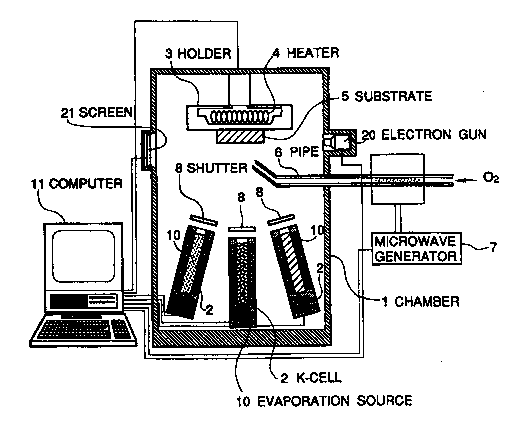
Fig. 1 illustrates a simplified MBE machine which is used for
producing the compound oxide thin film according to the present
invention.
Fig. 1 shows essential parts of a molecular beam epitaxy (MBE)
machine which is used in the present invention. All details of a pressu~e
sensor in ~e chamber, manipulators, evacuation pumps or the like are
omitted for clarity and because they are well-known. The MBE machine
shown in Fig. 1 has a chamber (1) which can be evacuated to a high
vacuum, a plurality of evaporation cells (2) such as Knudsen Cells each
containing an evaporation source (10) or an element to be evaporated
which are heated adjustably to desired temperatures, shutters (8) each
being actuated independently and in a predetermined order so that the
amount of each atom beam evaporated from the evaporation cell (2) is
controlled, a substrate holder (3) equipped with a heater (4) whose
2 0 temperature is controllable, a pipe (6) for introducing active gas such as
oxygen gas which is opened in the neighborhood of a surface of a
substrate (5) on which a thin film is deposited, a microwave generator (7)
for exiting the active gas in the pipe (6), and an analyzer for monitoring a
crystal structure of the thin film on said substrate such as RHEED
2 5 analyzer consisting of an electron gun (20) and a screen (21).
The process according to the present invention can be carried out
by operation the MBE machine manually. Followings are two examples
. ;~
.;
:.~. .9 .
...
i
.. ; ;
:". ,~ , J
',' ` , ~ ': `'
.~ :
`'` ' ' ` ' `' ~: `
' ' , ' ' .' ,':
'~''' j , ~ ' :
" . '' ` ,: '
"' ~ ' ' ' ''
:.'`- ' , ' ~ ' ' ~
2029038
of manual operation when thin films of superconducting oxides:
YlBa2Cu307 z and Bi4Sr4Ca4Cu6016+~ (=2 Bi2sr2ca2cu3o8+8l2) are
prepared.
A layered superconducting oxide of YlBa2Cu307 z has a unit
5 crystal which consists of a Ba-O layer, a Cu-O layer, a Ba-O layer, a Cu-
O layer, a Y-O layer, a Cu-O layer, a Ba-O layer, a Cu-O layer and a Ba-
O layer stratified in this order. When a thin fflm of YlBa2Cu307 z is
vi deposited on a substrate by manual operation, beams of vapour sources
(10) each being an elemental metal of Y, Ba and Cu heated in a respective
K-cell (2) are directed to a substrate (5) in a predetermined order by
shuttering respective shutters (8), while excited oxygen gas is supplied to
a surface of the substrate from the pipe (6), so that the above-mentioned
Ba-O layer, Cu-O layer, Ba-O layer, Cu-O layer, Y-O layer, Cu-O layer,
Ba-O layer, Cu-O layer and ~a-O layer are deposited successively in ~is
order. This stage is called "film-folming operation". According to the
present invention, after lamination of one unit crystal complete, the film-
forming operation is interrupted and a crystallization promotive operation
is effected. In actual operation, all shutters (8) are closed and the
constituent layers deposited are left in an atmosphere of oxygen gas which
O is supplied continuously through the pipe (6). During this crystallization
promotive operation, rearrangement of elements or ordering of the
crystal is realized. Timing of termination of the crystallization promotive
~'? operation can be detected by monitoring output signal of the reflection
; high energy electron diffraction (RHEED) analyzer. In the case of
7 25 superconducting oxide of ~1Ba2Cu307.z, the crystallization promotive
operation is terminated when a unique streak pattem caused ~y such a fact
- that the crystal has a longer lattice constant along b-axis than a~ong a-axis
.
,
,
2029038
is observed in the RHEED pattern. After the crystallization promotive
operation complete, next film-forming operation is restarted. A
combination of the film-forming operation and the crystallization
promotion operation is repeated for desired times until a desired film
~; S thickness isobtained.
.~ A layered superconducting oxide of Bi4sr4ca4cu6ol6+~ (= 2
.,7,' Bi2Sr2Ca2Cu30g+~2) has a half (1/2) unit crystal which consists of a Bi-O
, layer, a Sr-O ~ayer, a Cu-O layer, a Ca-O layer, a Cu-O layer, a Ca-O
;~ layer, a Cu-O layer, a Sr-O layer and a Bi-O layer stratified in this order.
s 10 One unit crystal is made by two of the half unit crystal which are
deposited symmetrically. When a thin film of B4Sr4Ca4Cu6016~ is
deposited on a substrate by manual operation, it is preferable to carry out
i~ the crystallization promotion operation after half unit crystal is layered in
:~ the film-forming operation because numbers of constituent layers
15 corresponding to one unit crystal are rather too lager to facilitate the
ordering of crystal so that it is difficult to obtain a desired crystal
structure composed mainly of a high-temperature phase of this
;~ superconducting oxide. In actual operation, beams of vapour sources (10)
each being an elemental metal of Bi, Sr, Ca and Cu heated in a respective
2 0 K-cell (2) (in this case the numbers of K-cells are increased to four) are
directed to a substrate (S) in a predetermined order by shuttering
respective shutters (8), while excited oxygen gas is supplied to a surface
:}
- ~ of the substrate from the pipe (6), so that the above-mentioned constituent
layers of Bi-O layerf Sr-O layer, Cu-O layer, Ca-O layer, Cu-O layer,
2 5 Ca-O layer, Cu-O layer, Sr-O layer and Bi-O layer which correspond to
. the halt unit crystal are deposited successively in this order. According tO
~ the present invention, after lamination of half unit crystal complete, the
,
-11-
, .,
~.,
:~ ,
.
s,
.~ .
.'. ' '. :' ' ' '
2029038
film-forming operation is interrupted and a crystallization promotive
operation is carried out by closing all shutters (8) and deposited
constituent layers are left in an atmosphere of oxygen gas which is
supplied continuously through the pipe (6). During this crystallization
5 promotive operation, rearrangement of elements or ordering of the
crystal is realked. Timing of termination of the crystallization promotive
operation can be detected by monitoring output signal of the RHE~D
analyzer. In the case of superconducting oxide of Bi2Sr2Ca2Cu308+~12,
;, the crystallization promotive operation is te~ninated when a specific10 modulation pattern which is unique to the high-temperature phase of this
oxide is observed in the RHEED pattern. After the crystallization
3 promotive operation complete, next film-forming operation is restarted.
A combination of the film-forming operation and the crystallization
~ promotion operation is repeated for desired times until a desired film
7 15 thickness is obtained.
When the process according to the present invention is automated
by the computer-aided system according to the present invention, the
crystallization promotion operation is controlled by the computer (11)
which is programmed as following:
~ 20 (1) a pattern which is created by the electron gun (20) on a screen (21)
'J', iS transformed into electric image signals by an image processor (notshown). The electric image signals are input in the computer (11) and are
compared with known image data of an oxide concemed whi~h are stond
in the computer,
i, 25 (2) the deposited constituent layers are left in an activated oxygen
atmosphere in order to effect a crystallization promotive operation until
;-:
12-
,
!.
" :
..i,
` '; '. ' `
' . , ' ~ ~ I
: :
" . ` ~ . '
2~29038
.
the electric image signals from the image processor become equal to ~e
known image data,
1 (3) after the electric image signals from the image processor become
i equal to the known image data, next film-forming operation is restarted,
~( 5 and
.~ (4) a combination of the film-forming operation and the crystallization
.~3 promotion operation is repeated for desired times until a desired film
thickness is obtained.
In a preferred embodiment of the system according to the
invention, all sequence during the film-forming operation and the
crystallization operation are proceeded according a program input in the
? computer (11). In this case, all operational parameters including a flow
rate of oxygen gas (6), an energy of the microwave generator (7),
temperature of the su~strate heater (4), temperature of K-cells (2) and
order and time duration of shutters (8) in the film-forming operation are
memorized in the computer previously, so that all operations in the film-
forming stage are carried out automatically under a control of the
computer according to a programed feed-back control sequence which is
well-known in the computer control system.
2 0 According to the present invention, thin films of oxide
superconductors of high quality can be obtained owing to the
' crystallization promotion operation which is interposed between
::: successive film-fonning operations.
The process according to the present invention can be carried out in
, 2 5 h~own MBE machine without changing the machine and is advantageously
operated automated condition by using a computer.
.:
''~,
:~ ~ 13-
,
~;
;~ ,
~ '; '~ ' -
., , ., ~.. : . ,
-- 2029038
Now, examples of the present invention will be shown but the
present invention should not be limited to the special exarnples.
. . .
.~, ~Q~
S A thin ~llm of YBa2Cu307 z was deposited on a {100) plane of a
single crystal of MgO according to the process of the present invention in
the MBE machine shown in Fig. 1. In this example, the computer (11)
~;~ was not used but the operation was carried out in manual control.
Oxygen gas was exited by the microwave generator (7) and was
,";1
supplied from the pipe (6) in the neighborhood of a surface of the MgO
substrate (5). K-cells (2) each containing elemental metals of Y, Ba and
Cu were heated to temperatures of 1,450 C for Y, 500 C for Ba and
1,080 C for Cu. A~er ~en, a fllm-forming operation was started.
In the film-forming operation, after the -chamber (1) was evacuated
,~. 15 to a pressure of 5 x 10⁻⁶ Torr and the substrate (5) was heated to a
temperature of 650 C, shutters (8) were opened in an order of Ba, Cu,
Ba, Cu, Y, Cu, Ba, Cu and Ba to deposit constituent layers corresponding
to one unit clystal. Shutters were opened for 4 sec in Y, for 3 sec in Ba
and for S sec in Cu respectively.
Then, a crystallization promotive operation was carried out by
monitoring the RHEED analyzer. During the crystallization promotive
~; operation, the pressure in the chamber and the substrate temperature was
maintained at the same values as those of the film-forrning operation,
namely S x 10-6 Torr and 650 C until an a-axis became shorter than b-
2 5 axis in a RHEED pattern.
After this condition was realized, the film-forming operation was
" restarted. Then, a combination of the film-forming operation and the
, .--
14 -
. ~ .
: ~"
x~ 1
~:s
202~038
crystallization promotive operation was repeated until a desired film
~ickness of 100 nm was obtained.
For comparison, the film-forming operation alone was repeated
without interposing the crystallization promotive operation of the present
S invention to prepare a thin film of 100 nm thick according to know
process. Film forming speed of the comparative example was 0.5 A/sec.
Common conditions to the present invention and the comparative
example are as following:
Substrate temperature: 650 C
Pressure in the chamber: S x 10-6 Torr
3 Flow rate of acthated oxygen: 0.5 SCCM
,~
Pressure in the oxygen supply pipe
at the microwave discharge zone: 0.5 Torr
Superconducting properties (Tc = critical temperature, Jc = critical
15 current density) of thin filrns obtained are summarized in Table 1.
Table 1
., Power of Tc Jc * Appearance
2 0 microwave (W) (K) (A/cm2) of surface
.~
Invention 150 88 2.4 X 10⁶ smooth
Comparative 150 82 0.9 X 10⁴ uneven
(~); determinedat77K
The result revealed that the thin film prepared by d~e process
;. according to the present invention is improved in surface condition and in
1 crystallinity and hence is of high quality.
~'
. .,
.~! ' 15 -
.,.
!'l
:~
,' ., ` .
:'.................................. . .. .
s - 2~290~8
~ixam~le ~
Example 1 was repeated to prepare a ~in film of YBa2Cu307 z on
a (lOOJ plane of a single crystal of MgO in the MBE machine shown in
. Fig. 1, but, in this example, a~l operations were programed in the
computer (11) in which the following data were input previously:
; Film~forming o~eration
Temperature of K-cells: Y = 1,450 C, Ba = 500 C
Cu = 1 ,080 C
:'~
~ Shuttering order : Ba, Cu, Ba, Cu, Y, Cu, Ba, Cu and Ba
1 0 Shuttering time duration: Y = 4 sec, Ba = 3 sec, Cu = 5 sec.
Pressure in the chamber: S x 10-6 Torr
Substrate temperature: 650 C
. Flow rate of activated oxygen: 0.5 SCCM
Pressure in the oxygen supply pipe
atthe microwave dischargezone: 0.5 Torr
. Film thickness: 100 nm
Crystallization promotive operation
. Pressure in the chamber: 5 x 10⁻⁶ Torr
Substrate temperature: 650 C
2 0 ~low rate of activated oxygen: 0.5 SCCM
Pressure in the oxygen supply pipe
; at the microwave discharge zone: 0.5 Torr
RHEED pattern data: A streak pattern of known crystal
` structure of YBa2Cu307.z was
,.
2 5 converted to digital image data
The film-forming operation was carried out automatically
~;according to the program. In the crystallization promotive operation, the
. .
~.~ 16-
...
. .,
-- , ,, , : . .
. i . . . .: .. . - , .
2029038
-- computer (11) was programed such a manner that output signals of the
i RHEED analyzer were processed by an image processor to produce image
- data which were compared with the streak pattern data of known
;~j superconducting oxide of YlBa2Cu3O7.z stored in the computer (11) and
''.','.~7,' 5 dlat timing of termination of the crystallization promotive operation was
determined when both data became substantially identical, more precisely
when distances of a-axis and distances of b-axis became identical.
The result of superconducting properties of thin film obtained are
summarized in Table 2.
Table 2
;~ ReacdonPower of Tc Jc *
~ Gasmicrowave (W) (K) (Alcm2)
.,~
~ 1 5 Oxygen 150 88 2.4 X lo6
~,,
determined at 77 K
The thin f11m obtained showed improved surface condition and
.. ~ crystallinity and hence was of high quality.
2 0
Example 3
A thin film of Bi2Sr2Ca2Cu3Og+~/2 was deposited on a 1100~ plane
of a single crystal of MgO according to the process of the present
invention in the same MBE machine as Fig. 1, but numbers of K-cells (2)
` ' 2 5 were increased to four. In this example, the computer (11 ) was not used
but the operation was carried out in manual control.
' Oxygen gas was exited by the microwave generator (7) and was
'j supplied from the pipe (6) in the neighborhood of a surface of the MgO
substrate (5). K-cells (2) each containing elemental metals of Bi, Sr, Ca
~ -17
~j
. .~ ..
, '! S
'~ :
' '. ' i ' ~, ,: ~ ` ' :
,~' ~, . , ' :
,.;,; . ' ' '' . ~ ` :
~ 202~03~
and Cu were heated to temperatures of 530 C for Bi, 500 C for Sr, 520
C for Ca and 1,100 C for Cu. After dlen, a film-forming operation was
.,
started.
.. J In the film-forming operation, after the chamber (1) was evacua~ed
s~ 5 to a pressure of 5 x 10⁻⁶ Torr and the substrate (5) was heated to a
.~ temperature of 650 C, shutters (8) were opened in an order of Bi, Sr,
~ Cu, Ca, Cu, Ca, Cu, Sr and Bi to deposit constituent layers corresponding
?1 to a half unit crystal. Shutters were opened for 2 sec in Bi, for 3 sec in
Sr, for 4 sec in Ca and for 3 sec in Cu respectively.
-~ 10 After constituent layers corresponding to a half unit crystal was
layered, a crystallization promotive operation was carried out by
' monitoring the RHEED analyzer. During the crystallization promotive
operation, the pressure in the chamber and the substrate temperature were
, maintained at the same values as those of the film-fo~ning operation,
name}y 5 x 10⁻⁶ Torr and 650 C until a specific modulated RHEED
paKern which is unique to the crystal of Bi2Sr2Ca2Cu3Og+d/2 was
.i observed on a monitor.
After this condition was realized, next film-forming operation was
.. restarted. Then, a combination of the film-forming operation and the
~J 20 crystallization promotive operation was repeated until a desired film
thickness of 100 nm was obtained.
For comparison, the film-forming operation alone was repeated
without intelposing the crystallization promotive operation of ~e present
invention to prepare a thin film of 100 nm thick according to know
` ~ 2 5 process. Film fonning speed of the comparative example was 0.5 A/sec.
, Common conditions to the present invention and the comparative example were as following:
~ .
~ -18-
:,~
. .
!........... , , , , `:. -'. .:.. '.' '. ': :
- 2029038
,
Substrate temperature: 650 C
Pressure in ~e chamber: 5 x 1~6 To~r
~J~ Flow rate of activated oxygen: 0.5 SCCM
Pressure in ~e oxygen supply pipe
at~emicrowave dischargezone: 0.5 Torr
Superconducting properties (Tc, Jc ) of thin films obtained are
summarized in Table 3.
,
Table 3
Power of Tc Jc * Appearance
microwave (W) (K) (A/cm2)of surface
. .
~. Invention 150 108 2.8 X 10⁶smooth
,.,,~
Comparative 150 92 0.9 X 10⁴uneven
detennined at 77 K
The result revealed that the thin film prepared by dle process
;.,; according to the present invention is improved in surface condition and in
,.~
2 0 crystallinity and hence is of high quality.
~xample 4
Example 3 was repeated to prepare a thin film of
Bi2Sr2Ca2Cu3O8~d/2 on a ~100) plane of a single cr,vstal of MgO in the
'j 2 5 same MBE machine as Fig. 1, but the numbers of K-cells were increased
to four and all operations were programed in the computer (11) to which
the following data were input previously:
Eilm-forming o~eration
Temperature of K-cells: Bi = 530 C, Sr = 500 C
:
.19.
., .
.~ ', ' ." ~
~'j'' ' ' : . ':
;~;,"' ~ ' ' :
202~03~
: ~ Ca = 520 C Ca = 1,100 C
Shuttering order : Bi, Sr, Cu, Ca, Cu, Ca, Cu, Sr and Bi
-~ (=numbers of constituent layers
corresponding to a half unit crystal)
Shuttering time duration: Bi = 2 sec, Sr = 3 sec,
Ca - 4 sec Cu = 3 sec.
Pressure in the chamber: 5 x 10⁻⁶ Torr
Substrate temperature: 650 C
Flow rate of activated oxygen; 0.5 SCCM
Pressure in ~e oxygen supply pipe
at the microwave discharge zone: 0.5 Torr
Film thickness: 100 nm
~rystallization promotive operation
Pressure in the chamber: S x 10-6 Torr
. 1 5 Substrate temperature: 650 C
~. ~low rate of activated oxygen: 0.5 SCCM
;~ Pressure in the oxygen supply pipe
~` at ~e microwave discharge zone: 0.5 Torr
`1 RHEED pattem data: A streak pattern of known crystal
'!~ 2 0 structure of Bi2sr2ca2cu3o8+dl2
was converted to digital image data
The film-forming operation was carried out automatically
. according to the program. In the crystallization promotive operation, the
computer (11) was prograrned such a sequence that output signals of the
2 5 RHEED analyzer were processed in an image processor to produce image
data which were then compared with the streak pattern data of known
superconducting oxide of Bi2Sr2Ca2Cu3Og+d/2 stored in the computer
,~,
~ -20 -
;.,
.;~
,, . . . :
2029038
(11) and that the crystallization promotive operation was terminated when
bo~ data became identical, more precisely when a speci~lc modulated
pattem which is unique to the crystal of Bi2sr2ca2cu3o8+d/2 was
. obtained in the RHEED.
'2? 5 The result of superconducting properties of thin ~llm obtained are
summarized in Table 4.
Table 4
f
Reaction Power of Tc Jc *
10 Gas microwave (W) (K) (A/cm2)
.,
Oxygen 150 108 2.8 X 10⁶
(*): detelmined at 77 K
The thin film obtained showed improved surface condition and
crystallinity and hence was of high quality.
~.
,~,
;:~
... .
.,
,~
.~ .
, 1
-21 -
~'`;
... .
... ~i .,
.~? ' . ~ .~
~:~ . . ,. : ,
. ::. . , ,,, , :: ,