Note : Les descriptions sont présentées dans la langue officielle dans laquelle elles ont été soumises.
PHD 89204 1 8.11.1990
Receiver with direct quadrature sampling of the input
signal.
The invention relates to a receiver in
which a normal component and a quadrature eompanent of a
signal that is modulated on a carrier signal are
directly generated by sampling the carrier signal, the
sampling instant being determined by a sequence of
sampling instants.
In the article entitled '°Quadrature
Sampling of FM-Bandpass Signals ° Implementation and
Error Analysis'°, W. Rosenkranz, Pros. of the Int. Conf.
on Digital Signal Processing, Florence, Ttaly, 1987, pp.
377 to 381, the sampling is described of frequency-
modulated bandpass signals in which the real and
imaginary parts of the complex envelope, the so-called
quadrature components, are directly produced by sampling
the modulated bandpass signals at a carrier frequency f~.
For this purpose, an analog-to-digital converter is
controlled by means of periodically recurrent sampling
pulses having a frequency f~, to be denoted as clock
frequency fQ hereinafter.
The clock frequency f9 is to be selected
in such a way that a sampling interval Te for sampling
the normal component, i.e. the real part of the bandpass
signal, exactly corresponds to a half wavelength of the
carrier frequency or an integer multiple of this time
interval respectively. With odd multiples, however, the
sign of each second sample value can be inverted. In
order to produce sample values of the quadratuxe
component which is in quadrature to the sample values of
the normal component thus produced, the input signal is
to be sampled at instants which with respect to the
sampling instants of the normal component present a
time-delay of a quarter of the carrier signal wavelength
or a quarter plus an integer multiple of the half
PHD 8920 2 8.11.1990
carrier signal wavelength. Also in this case with add
multiples the sign of each second sample value can be
inverted. In this manner value pairs will be obtained
corresponding to a sampling frequency of fa = 1/T, which
correspond to the real and imaginary parts of the
complex envelope.
In a circuit arrangement described in the
article mentioned hereinbefore only a single analog-to-
digital converter is necessary. The clock frequency fQ
is selected in such a way that the clock interval Tq =
1/f9 is equal to a quarter of the wavelength plus an
integer multiple of the half wavelength of the carrier
frequency. Consequently, the two conditions mentioned
hereinbefore are alternately fulfilled so that each
sample value alternately corresponds to the normal
component and the quadrature component. Hy means of an
interpolation filter the time-delay of I arid Q
components obtained in pairs is eliminated so that
values corresponding to those of a simultaneous sampling
of I and Q components are obtained at the output of the
filter. Thus, the ratio of the carrier frequency fyto
the half sampling frequency fe/2 is an integer and cannot
be chosen arbitrarily.
A further condition is that the sampling
frequency fa is at least equal to the bandwidth B of the
bandpass signal to be sampled.
With bandpass signals whose signal of
which 'the content is derived from a sequence of binary
values based on a bit clack frequency fb, it is
advantageous for the sampling frequency fa to be chosen
to be equal to the bit clock frequency fb.
In transmission systems in which, for
example, this bit clock frequency fb is a predetermined
value, the choice of the carrier frequency fc in prior-
art arrangements is thus considerably restricted by the
described items.
It is an object of the invention to
2~~~~Q~
PHD 89204 3 8.11.1990
extend the selection possibility from the available
carrier frequencies in a receiver of this type.
This object is achieved in that a
plurality of equidistant sampling instants are combined
to a group and in that for the distance in time between
the last sampling instant of a group and the first
sampling instant of the next group (group distance) an
interval is selected different from the distance in time
between two successive sampling instants within a group.
By means of the selectable group distance
the length of a sampling interval T,, corresponding to
the distance between a first sampling instant of a group
and the first sampling instant of the next group (group
length), can be selected arbitrarily. This is
advantageous in that the sampling interval and the
carrier frequency can be adapted to each other by
appropriately selecting the group distance. By means of
equidistant sampling instants within the group of
sampling instants the normal and quadrature components
are further obtained in prior~art manner. By accordingly
selecting the group distances, a phase rotation develops
between corresponding sample values of successive
groups. This phase rotation may be eliminated by means
of a further processing of the sample values.
If the group distance is selected in such
a way that it corresponds to a multiple of a quarter of
the wavelength of a carrier signal, said phase rotation
will correspond to a multiple of 90°. This is
advantageous in that the subsequent processing is
reduced to an inversion of the sample values and, i;E
necessary, to an inter- changing of the. sample values.
Since inversions and interchanges can be performed in a
relatively simple manner, the subsequent processing
entails only little circuitry and cost in this
embodiment.
By selecting individual group distances
differing from one group to the next, even these
- 4 - 20104-8676
interchanges and, if necessary, also the inversions can be omit-
ted. In another application the mutually different group
distances may produce sample values present each a different
phase rotation. As will be further explained in an exemplary
embodiment, the further processing of the .received signals may
thus be simplified.
The invention will be further described and explained
in 'the following with reference to the exemplary embodiments
shown in the drawings, in which:
Figure 1 shows a block diagram for a receiver having
direct quadrature sampling;
Figure 2, comprising parts 2a to 2f, shows a sampling
pulse sequence and various switching-signal -time diagrams for
8-bi-t oversampling of an input signal in a bit interval of 158
basic clock signals and a periodic continuation of the sampling
pulses'after each bit iwterval;
b'igure 3a shows sample values after sa~tpling;
Figure 3b shows sample values after interpolation;
Figure 3c shows sample values after taking the mean
values;
Figure 4, comprising parts 4a to 4f and 4a' to 4f',
shows sampling pulses and various switching-signal time diagrams
for 8-bit oversampling of an input signal in a bit interval of
158 basic clock signals and a periodic continuation of the
sampling pulses after 159 and 155 basic clock signals respec-
Lively.
._
- 4a - 20104-8676
In the following exemplary embodiments binary
encoded signals are started from, based on a bit rate of
fb = 270.833 kHz (= 13 MHz/48) and modulated on a HF carrier
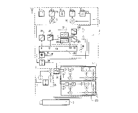
by means of angle modulation. Figure 1 shows in a diagram
a radio receiver consisting of a HF section 1, a quadrature
section 2 and an arrangement for digital signal processing 3.
In the HF section 1 the frequency of a
4~a~~~~~
PHD 89204 5 8.11.1990
received signal is selected and converted into a carrier
frequency. For this purpose, the signal received from a
HF receiving stage 11 is mixed down to a first
intermediate frequency ZF1 by means of a first IF mixer
12 to which is applied a first variable IF mixing
frequecy f~ by a first IF oscillator 13. The input
signal mixed down to this first intermediate frequency
is bandpass filtered in a first IF amplifier 14,
amplified and applied to a second IF mixer 15, in which
the input signal is mixed down to a second intermediate
frequency ZF2 by means of a second intermediate
frequency applied by a second IF oscillator 16. In a
second IF amplifier 17 this second intermediate
frequency ZF2 is again bandpass filtered and amplified.
The second intermediate frequency ZF2 is
applied to an analog-to-digital converter 21 in the
quadrature section 2. This analog-to-digital converter
21 is controlled by means of clock pulses f; generated by
a central clock generator 20. In this exemplary
embodiment the second intermediate frequency f~ is
selected in such a way that it corresponds to an integer
multiple of the half bit clock frequency fb. The value of
79 was selected as an integer ratio of second oscillator
frequency f~ to half bit clock fb. This yields a second
intermediate frequency of 10.6979166 MHz which is
advantageous in that this intermediate frequency only
slightly differs from the intermediate frequency of 10.7
MFIz used in 'the radio range. This is advantageous in
that commercially available filters can be inserted for
3U this selected intermediate frequency f~.
In a central clock controller 20 a clock
generator 201 is arranged which generates a basic clock
of a quarter. of 'the wavelength of the second
intermediate frequency fZ~. Deviations from the provided
frequency ratio of the second intermediate frequency ZF2
to the basic clock result in a frequency mistuning. Such
.frequency mistunings which are small with respect to the
1~HD 89204 6 8.11.1990
bandwidth of the signal can be tolerated with an
appropriately arranged subsequent signal processing.
However, it is more advantageous to eliminate such
frequency mistunings in advance. It is especially
advantageous to derive also the mixing frequency of the
second IF oscillator 16 from the clock generator 201.
This makes it possible to rigidly determine the
frequency response ratio of the second intermediate fre-
quency ZF2 to the basic clock independent of external
influences.
In this exemplary embodiment 158 basic
clock signals correspond exactly to a bit clock having
the bit frequency fb. This basic clock signal is applied
to a counter 202. This counter 202 generates the
sampling pulse f; at each ninth basic clock signal.
Consequently, two adjacent sample values are exactly 24
wavelengths of the second intermediate frequency ZF2
apart. The counter generates a total of exactly
seventeen of these equidistant successive sampling
pulses within one bit clock. These seventeen successive
sample values thus form a group of equidistant sample
values. A sampling pulse which might occur at the 153rd
basic clock is suppressed so that exactly nine sample
values for the normal component and eight sample values
for the quadrature component can be contained in each
bit clock in this manner. After 158 basic clock signals
the counter is reset and the clock generation for the
sampling pulses f; is resumed as described hereinbefore.
In this manner the sequence of the generated sampling
pulses f; is periodically continued after each 158th
basin clock signal.
Between the last sample value of a group
of sample values and the first sample value of the next
group of sample values there are exactly 14 basic clock
signals. The groups thus follow each other 14 basic
clock signals apart. In this exemplary embodiment the
distance between the groups is chosen larger than the
PHD 89204 7 8.11.1990
distance between two successive sample values within one
group. However, the group distance can also be chosen to
be smaller than the distance between two successive
sample values within a group provided that a
correspondingly fast analog-to-digital converter is
used.
The technical implementation of counters
is known to those skilled in the art of digital
electronics. One of the possible embocliments of such a
counter can be taken from Chapter 10.7 "Systematischer
Entwirrung von Schaltwerken°' of the title
"Halbleiterschaltungstechnik", U. Tietze, Ch. Schenk,
Springer verlag Herlin, 8th edition, pp. 259 to 268. In
the following the technical realisation of the counter
25 201 is hence not further explained. Tnstead, time-
voltage diagrams for the individual switching signal
outputs of the counter 201 are represented in separate
Figures for a further description of the counter 201.
Fig. 2a represents an unmodulated carrier
oscillation fC, the bottom portion of Fig. 2a showing a
time axis and each basic clock signal being represented
by a line through the time axis. Fig. 2b represents the
sampling pulses f; generated by the counter 201 and
starting at the basic clock signal 0. Clearly noticeable
is the gap between the seventeenth sampling pulse
accounting for the 144th basic clock signal of the first
bit clock and the next sampling pulse f; accounting for
the first basin clock signal of the next bit clock (_
158th basic clock signal). Since the distance in time
between the sampling pulses f; is selected in such a way
that this distance is exactly equal to 2a wavelengths of
the second intermediate frequency 2F2 as described
hereinbefore, 'these sampling pulses alternately cause
sample values of the normal and of the quadrature
components to occur. The alternately succeeding sample
values of a bit clock period of the normal and the
quadrature components are alternately allocated, by
PHD 89204 8 8.11.1990
means of a component allocator 22, to a first signal
branch for processing the normal component and to a
second signal branch for processing the quadrature
component by means of a component allocator 22
symbolically shown in the drawing as a change-over
switch. An appropriate switching signal Q1 for
controlling the component aliocator 22 is also generated
by the counter 202. The component allocator 22 is
structured in such a way that the allocator applies the
sample value present at an input to the first signal
branch for processing the normal component when there is
a low voltage level (low signal) at the switch input and
applies the sample value present at the input to the
second processing branch for processing the quadrature
component when theme is a high voltage level (high
signal) at the switch input. The voltage variation of
the switching signal Q1 that controls the component
allocator 22 is represented in Fig. 2c. It is clearly
noticeable that the switching signal Q1, starting at the
0th basic clock signal, with a "low" signal alternately
changes its voltage level from low to high and vice
versa every ninth basic clock signal. At the beginning
of the next bit clock, in the exemplary embodiment and
in Fig. 2a the basic clock signal number 158, the signal
variation of the switching signal Q1 corresponds to that
in the previous bit clock.
Since the distances between two sample
values of the normal component and two sample values of
the quadrature component thus correspond to odd
multiples of the half wavelength of the second
intermediate frequency f~, each second sample value of
the normal component and each second sample value of the
quadrature component is to be invexted. For this
purpose, a sign inverter 231, 232 and a change-over
switch 233, 234 are arranged in each signal branch.
These change-over switches 233, 234 are structured in
such a way that, if there is a "low" signal at their
FHD 89204 9 8.11.1990
inputs, the sample values of the processing branch
concerned are canveyed directly whereas, if there is a
"high" signal at their inputs, the sample values are
conveyed to the sign inverters 231, 232. The variation
of a second switching signal Q2 that controls the first
change-over switch 233 is shown in Fig. 2d and the loss
of a third switching signal Q3 that controls the state
of the second change-over switch 234, is represented in
Fig. 2e. The second and third switching signals Q2, Q3
also produced by the counter 202 are selected in such a
way that the sample value and the inverted sample value
for each second sample value is alternately conveyed in
each signal branch. Fig. 3a symbolically shows the
sample values of a modulated signal obtained after the
sign inversion, the normal components having an x at the
top and the quadrature components an o at the top.
Although normal and quadrature components are processed
in separate signal branches, they are shown together in
Fig. 3 so as to clarify their mutual allocatian in time.
From Fig. 3a it is evident that a sample value of the
quadrature component controlled in time is always
situated in the middle between two sample values of the
normal component.
In an interpolator 25 the normal
component is filtered. Since the sample values taken
into account for the interpolation are equidistant and
close together, the structure of the interpolator is
thereby simplified and the interpolation result
improved. In the exemplary embodiment a linear
interpolator is used which farms an interpolation value
from two succeeding sample values.
In the interpolator 25 each last sample
value is buffered in a register. The buffered sample
value and the sample value just present at the input are
divided in two, for example, by shiftincJ the bit pattern
one position to the left, and then added together. The
value interpolated in this fashion corresponds in a
PAID 89204 10 8.11.1990
proper approximation to a sample value which would have
been obtained midway between the two last sample values
applied to the interpolator. In this fashion tine
interpolated sample value of the normal component and
the sample value of the quadrature component sampled
between the last two sample values of the normal
component applied to the interpolator 25, can be
considered to be sampled simultaneously.
Since the result of the interpolatar 25
is always obtained only after the last two applied
sample values have been processed, the associated sample
value of the quadrature component is to be delayed in
time by means of a delay element 24 in order to realise
simultaneity between interpolated sample value and
associated quadrature component during the fuxther
processing. This time delay corresponds exactly to the
distance between two regularly succeeding sampling
pulses f;, that is to say, 9 basic clock signals in the
exemplary embodiment. As a result of the interpolation
eight interpolated sample values are formed from the
nine sample values of the normal component of a bit
clock signal (cf. Fig. 3b). A switch 26 controlled by a
fourth switching signal Q4 prevents that an interpolated
value formed after the ninth sample value is conveyed
(cf. signal variation of the switching signal Q4 in Fig.
2e). Due to the delay of the interpolator output signals
caused by the interpolation, the switching signal Q4 is
generated delayed over exactly this delay period.
Fig. 3b shows how eight interpolated
sample values of the normal component are obtained from
the nine sample values of the noxrnal component.
The eight interpolated sample values of
the normal component and the eight sample values of the
quadrature component are applied each to its own mean
determining filter 271, 272. In the filters 271, 272 a
single value for the normal component or quadrature
component respectively, is produced from the eight
PHD 89204 11 8.11.1990
sample values. As a result of the 8-bit oversampling the
quantization noise of the analog-to-digital converter is
thus reduced by nine dB. In this manner exactly one
value for the normal component and the quadrature
component is obtained for each bit clock. Because of the
equidistance of the eight sample values also the
structure of the mean determining filter is simplified.
In the exemplary embodiment the sample values of a bit
clock signal multiplied by a factor of 1/8 are added
together in order to obtain the mean value of each
normal component and quadrature component of a bit
clack.
Fig. 3c shows how one mean sample value
signal is produced from eight sample values at the end
of a bit clock.
If the number of basic clock signals
accounting for one bit clock signal is a number
dividable by four without a remainder, the sign of the
result of taking the mean value of succeeding bit clock
signals is correct and the quadrature components
produced in above manner can be conveyed to the digital
signal processing without being additionally processed.
However, if there is a remainder of two per bit clock
when the basic clock signals are divided, as was the
case hereinbefore, the quadrature components produced in
above manner are to be inverted every second bit clock.
However, this can be realised advantageously in that
with each second bit clock signal the counter 201
generates the phase-shifted control signals far changing
the states of switches 231, 232 through 180°(cf. mane
specifically, 'the variation of the switching signals Q2,
Q3 during the basic clock signals 158 to 159), so that
in each second bit interval each non-inverted sample
value is inverted as yet and each sample value inverted
in the first bit interval is no longer inverted. In this
manner the switching signals Q2 and Q3 are continued
only after each second bit interval whereas the
PHD 89204 12 8.11.1990
switching signals Q1 and Q4 are continued after each
single bit interval.
If the number of sampling pulses per bit
clock is chosen in such a way that the number of sam-
pling pulses divided by four produces a remainder of
unity, the quadrature components rotate from one bit
clock to the next through 90°. The sample value of the
normal component I becomes the quadrature component Q in
the second bit clock, in the third bit clock the
inverted normal component -T and in the fourth bit clock
the inverted quadrature component -Q. This holds in like
manner for the quadrature component Q. If the number of
basic clock signals per bit clock is selected in such a
way that it produces a remainder of three when divided
by four, the quadrature components lag by 90° in phase
from one bit clock to the next.
Tf in the transmitter a non-linear angle
modulation such as, for example, a type of modulation
known as Gaussian Minimum Shift Keying (GMSK) or a type
of modulation known as Generalized Tamed Frequency
Modulation (GTFM) is selected, the circuitry which is to
be used for signal equalization in the digital signal
processing section 3 can even be reduced. With such
types of modulation the complicated structure of a non-
linear angle modulation need no longer be taken into
account but the equalization can be restricted to the
case where a linear amplitude modulation was used during
transmission. Consequently, for equalization arid
demodulation only real numerical values are to be
processed in the digital signal processing section 3.
In the following an exemplary embodiment
is briefly described for such .a rotation of the
quadrature components. Gn the basis of the same bit
frequency fb ---- 270.833 kHz the number of basic clock
signals per bit interval Ta is selected to be 159. With
this number there is a remainder of three when four is
the divisor, so that the requirement as to the rotation
pfID 89204 13 8.11.1990
is fulfilled. Thus, the second intermediate frequency
ZF2 will be 159*(fb/4) = 10.?6562 MHIIz~ a frequency which
is still near to 10.7 ~iliz. When retaining the distances
between the sampling pulses f; the counter 201 produces
the same switching signals Q1, Q2, Q3 and Q4 whereas
after each 158th basic clock signal an additional 159th
basic clock signal is inserted per bit interval, whilst
all switching signals Q1, Q2, Q3 retain the same signal
condition as in the previous basic clock signal 158. Due
to the rotation the switching signals in the succeeding
bit intervals remain the same and are periodically
repeated after each bit interval T,.
If the quadrature components having the
correct phase are still necessary for the signal
processing, this rotation can be eliminated in an ernbo-
diment of the invention in which the number of basic:
clock signals per bit interval divided by four produces
an odd remainder, by mixing and/or inverting the
components per bit clock. This can be performed, for
example, by processing the quadrature components again
in that they are applied to a switch (not shown) which
interchanges the normal component and the quadrature
component in each second bit interval T,. The still
necessary inversions can be performed by merely
accordingly driving the change-over switches 233, 234.
In a further exemplary embodiment shown
in Fig. 4, as in the first exemplary embodiment, the
second intermediate frequency ZF2 is selected in such a
way that a bit interval is equal to 158 basic clock
signals. The time-dependent position of the sampling
pulses and switching signals for four succeeding bit
intervals are shown. The sampling pulses f; and switching
signals of the first bit interval (= basic clock signals
o to 158 in Fig. 4) correspond to the sampling pulses
and switching signals during the first bit interval in
the first exemplary embodiment. Tn this exemplary
embodiment the periodic continuation of the sampling
~2~~~~
PHD 89204 14 8.11.1990
pulses and the associated switching signals is delayed
in three succeeding bit intervals by one basic clock
signal and in a succeeding fourth bit interval shortened
by three basic clock signals. Consequently, the first
sampling pulse of the second bit interval (= basic clock
signals 158 to 316 in Fig. 4) is not situated at the
first basic clock signal as in the preceding exemplary
embodiments but at the second basic clock signal of the
second bit interval (= basic clock signal 159 in Fig.
4b). From Fig. 4a it is evident that, compared to the
first exemplary embodiment (cf. Fig. 2a)., the sampling
is effected a quarter period of the carrier frequency
later. Consequently, the inverted quadrature component
is obtained during the sampling with the first sampling
pulse in the second fait interval. The second sample
value in the second bit interval provides a sample value
for the normal component. Similarly holds for the other
sample values in the second bit interval.
In the third bit interval (= basic clock
signals 31& to 4?4 in Fig. 4b°) again the sampling pulse
sequence and the associated switching signals are
continued delayed by a basic clock signal. The first
sampling pulse of the third bit interval 'thus falls on
the third basic clock signal of the third bit interval
(= basic clock signal 318 in Fig. 4b°). Tn this case
Fig. 4a° shows that the first sample value of the third
sampling interval of the inverted normal component and
the second sample value of the third sampling interval
correspond to a sample value of the quadrature
component. The periodic sequence of the sampling pulses
is also continued in the fourth bit interval (= basic
clock signal 474 to 632) again delayed by a basic clock
signal. The first sampling pulse of the fourth sampling
interval thus corresponds to the basic clock signal 4??.
Tile sample value obtained with the first sampling pulse
in the fourth bit interval thus corresponds to the
sample value of a quadrature component and the second
PHD 89204 15 8.11.1990
sample value of the fourth bit interval corresponds to
an inverted sample value of the quadrature component.
In the initial three bit intervals the
period of the sampling pulses and the switching signals
Q1, Q2, Q3 is one basic clock signal longer than the
number of basic clock signals per interval, thus in this
exemplary embodiment is three times 159 basic clock
signals in succession. The distance in time between the
first sample value of the fourth bit interval and the
first sample value of the next bit interval in this
exemplary embodiment, however, is shortened by three
basic clock signals and accordingly amounts to only 155
basic clock signals. In this manner the first sample
sralue of the fifth bit interval is situated at basic
clock signal 632. The distance between the first
sampling pulse of the first bit interval and the first
sampling pulse of the fifth bit interval in this manner
exactly corresponds to four bit intervals (= 632 = four
times the 158 basic clock signals). In this manner a
sample value of the normal component will again be
obtained by means of the first sampling pulse of the
fifth bit interval. The variation of the sampling pulses
and the signal variation of the fifth sampling interval
henceforth corresponds to the first sampling znterval.
The order of the described sequence of
sampling pulses causes the sampling pulses in succeeding
bit intervals Ta to be shifted by a quarter of a period
of the second intermediate frequency ~F2. Consequently,
sample values of the I and Q components are alternately
applied to either of the twa branches. I and Q
components are alternately interpolated. After each
fourth bit interval there is a clock equalization as a
result of a sequence of sampling pulses shortened by
three basic. clock signals, so that the mean number of
basic clock signals per bit interval and the number of
output values of the quadrature signal generator are
equal compared to the first exemplary embodiment.
,..~
PHD 89204 16 8.11.1990
This exemplary embodiment is advantageous
in that the variation of the switching signals Q1, Q2,
Q3 remains the same in all four bit intervals. This
simplifies the structure of the counter. The counter is
reset three times in succession after 159 basic clock
signals and after these three longer basic clock signals
reset already after 155 basic clock signals.
In this manner also with bit intervals in
which the number of basic clock signals are an integer,
sample values rotating from one bit interval to the next
can be obtained. With the necessary changes having been
made this embodiment can also be implemented in arrange-
ments in which the number of basic clock signals per bit
interval is an odd number and in which the conseguerzt
effect of rotation of the sample values is to be
eliminated.