Note : Les descriptions sont présentées dans la langue officielle dans laquelle elles ont été soumises.
This invention relates to electronic flasher switches
which can be utilized in automotive applications, for example,
flashing turn direction indicators.
Various designs of flasher switches have been made in the
past. Thermal flasher switches incorporating a bi-metal
construction designed to be activated upon resistance heating
and expansion of metal components continue to be in frequent
use. Such units are popular due to relatively low cost of
manufacture. They may be of very simple construction,
requiring only a connector pin to the electrical supply and a
connector pin to the load. The supply may be either of
positive or negative polarity. Such switches may be operated
with two connection pins, but have frequently been provided
with another pole and a third pin to allow for additional
services to the automobile driver, such as the provision of an
independent dashboard light indicating serviceability of the
system. Disadvantages such as temperature sensitivity and
limited lifespan make thermal switches less favourable in a
wide variety of heavy duty applications such as in trucks.
Flasher switches incorporating single pole, single throw
relays have also been used. Again, these devices are
relatively robust. Such flasher switches have been designed
for operation under either fixed load or variable load
conditions.
With the introduction of sophisticated integrated
circuits, it became possible to control the operation of a
relay through an integrated circuit (IC). Flasher switches
utilizing this technology required three pins, since a ground
for the IC was necessary. Overload protection and short
circuit protection is normally regarded as necessary for such
devices. These devices were also strictly operable in
circuits of one polarity only. Thus, if such a device were
connected into a circuit "back to front", it would not
operate.
Nevertheless, such devices have various advantages. These
electronic flashers utilizing IC were, in their early
embodiment, unsuitable for the replacement of failed devices
unless these were of a similar design. One reason for this
was the necessity for utilizing three pins in the improved
device while the failed devices would be of the two-pin type
and hence suitable connections from the new device would not
be present. This difficulty was addressed in Canadian Patent
Application No. 595,229, filed March 30, 1989, inventor,
Rodney Hayden. That patent application described and claimed
a directional flasher switch incorporating an IC and designed
to operate without a ground so that only two pins are
required. The switch of that patent application is, however,
dependent on polarity and thus is not suitable for a
replacement part unless the wiring into which it is to be
incorporated is of proper polarity.
An attempt has now been made to provide a flasher switch
utilizing circuit having electronic relay control and which
may be tolerant to connection into a circuit of either
polarity.
According to the invention, there is provided a flasher
switch reversibly operable with a DC power source and a load
including: a first terminal adapted for connection to either
one of the DC power source and the load; a second terminal
adapted for connection to the DC power source when the first
terminal is connected to the load and to the load when the
first terminal is connected to the DC power source; a relay
connected to open and close a load circuit; drive means for
the relay having a positive input terminal for positive input
connected to each of the first and second terminals, a
negative input terminal for negative input connected to each
of the first and second terminals, and a sense input terminal
connected to each of the first and second terminals, the drive
means being adapted to open and close the load circuit in
response to signals applied to the sense input terminal; first
means to block transmission of negative signal to the positive
input terminal; second means to block transmission of positive
signal to the negative input terminal; and third means to
block transmission of signal other than that of a specific
relative polarity to the sense input terminal when the load
circuit is open and to present signal of a polarity opposite
to the specific relative polarity to the sense input terminal
when the load circuit is closed.
Suitably, the drive means is included in an integrated
circuit chip which may also include fault and overload
protection means. Such a chip may suitably be Motorola~ UAA
1041 or SGS Thomson~ 9686. It may also be possible to include
some or all the blocking means in an integrated circuit chip.
The blocking means may be, for example, diode bridges located
firstly between a V+ pin of the integrated circuit and each of
the first and second terminals arranged to block negative
signal to the positive pin, secondly between a -VCC pin of the
integrated circuit and each of the first and second terminals
to block positive signal to the negative pin, and thirdly
between a sensing pin and each of the first and second
terminals to block positive signal to the sensing pin from the
one of the first and second terminals that is connected to the
DC power source.
An embodiment of the invention will now be described by
way of example with reference to the accompanying drawings, in
which:
Figure 1 shows a prior art circuit for a flasher adapted
for use only with the polarity as indicated;
Figure 2 shows a modified circuit of Figure 1 for a
fixed load flasher switch, adapted, due to an
embodiment of the invention, for use with
polarity in either direction;
l' ;
Figure 3 shows a circuit modified in a similar manner to
that of Figure 2 but for a variable load
flasher switch;
Figure 4 shows a simplified circuit showing features of
the invention.
Figure 1 of the drawings illustrates a circuit diagram of
a prior art flasher switch. In fact, the circuit illustrates
a two-pin flasher switch as described and claimed in co-
pending Canadian Patent Application No. 595,229 hereinbefore
referred to. The circuit includes a positive source or
connection X and a lamp load L. Positive source X may be
connected to the positive terminal of an automotive battery
source (not shown). It is to be understood that in accordance
with the present invention, switching means (not shown) will
be present intermediate of the load L and the flasher switch
circuit, and that such switching means may include switches of
the 4-way hazard warning light type or of the directional turn
signal type. The lamp load L will vary according to the
number and types of operative automotive lamps connected in
the installed circuit.
With reference to Figure 1 showing a fixed load flasher,
positive source X is connected to a relatively low resistance
shunt 10. Shunt 10 is connected to both a relay contact 18
and terminal 7 on an integrated circuit 20. Integrated
circuit 20 may be of a type readily available to the
automotive parts manufacturing industry, such as model number
UAA 1041 manufactured by Motorola Semiconductor Products
Division of Motorola Limited. All IC pin numbers discussed
below correspond to pins 1 to 8 of the Motorola~ UAA 1041
integrated circuit, as would be known to a person skilled in
the art. As described herein, integrated circuit 20 may be of
a type providing overvoltage protection, fault detection and
other protective features.
S ~ ~ J ~
Terminal 7 is a fault detector pin for detection of, for
example, a shorted lamp socket. If a shorted lamp socket is
present in the circuit, a lower voltage is sensed at this
terminal if it is connected as shown and the signal switch
operation is prevented. However, if terminal 7 is not
connected, the switch will operate as variable load flasher
switch. Terminal pin 6 acts as an on-off switch for the fault
detector (overcurrent) feature. Where, as shown, terminal 6
is not connected to a positive voltage source, the fault
detector feature is in the on-position. Where this feature is
not desired, the terminal pin 6 should be connected to a
positive voltage source. It is to be understood that such a
feature is possible with fixed load flasher switches where a
unit will be designed to operate properly only when all of a
specified number of lamps are functional. In applications
where a variable load flasher switch is desirable, such a
fault detection feature is not possible as it is inherently
required that all remaining functional lamps be permitted to
flash upon activation of the switch. It is necessary that
positive source X is connected to the V+ pin 2 on the
integrated circuit 20 for proper operation of the integrated
clrcult .
In the embodiment shown, source X is also connected to
two capacitors 22 and 24 of differing sizes to allow for the
avoidance of using a separate ground and hence a third
terminal of the device. However, insofar as the present
invention is concerned, it is to be understood that the
circuit of Figure 1 is merely exemplary of a suitable circuit
onto which the present invention may be superimposed. The
concept of the present invention may equally be utilized for
three-pin devices.
Nevertheless, the operation of the circuit of Figure 1
will be briefly described by way of example. Capacitor 22 is
connected to V+ pin 2 and to diode 32 which acts to suppress
discharge of capacitor 22 across the lighting circuit, namely,
6 ~ 3 ~ z
the load L. Diode 32 is connected to resistor 11 which is in
turn connected to sensing terminal pin 8 on the circuit 20.
Pin 8 acts as a sensor for detection of the closure of relay
contact 18 through detection of a voltage level. Diode 30
serves a similar purpose to that of diode 32 by acting as a
gate to suppress discharge of capacitor 24 across the lighting
circuit. As shown, capacitor 24 is connected in series to
suppressor diode 30 as previously described and resistor 13 is
connected between pin 1 and capacitor 24. Resistor 13 is in
turn connected to pin 1 on integrated circuit 20, pin 1 being
the -VCC pin for the integrated circuit 20.
Initially, pin 8 senses a negative signal due to direct
connection of lamp load L. Such a negative signal at sensing
pin 8 allows energization of relay coil connected to pin 3 of
integrated circuit 20. Relay coil 40, when energized, closes
relay contact 18, allowing a positive signal to pass to pin 8.
Capacitor 26, which in conjunction with resistor 12
functions as a timer circuit, is connected to terminal pin 4
and resistor 12 which is in turn connected to terminal pin 5
of the integrated circuit 20. The flash rate of the flasher
switch circuit is a function of the features of the capacitor
26 and resistor 12. The capacitance rating of the capacitor
26 determines the time off of lights operating on the flasher
circuit and the corresponding resistance rating of resistor 12
determines the on time of such lights.
The operation of the flasher switch assembly through a
complete cycle may be described in generalized terms as
follows. Upon activation of a switch, such as a directional
turn signal switch or a hazard warning light switch (not
shown), a negative voltage is sensed at sensing pin 8. Timing
capacitor 26 is charged and once charged to capacity, relay
coil 40 is energized, thereby closing contact 18. Upon
closing contact 18, reversal in the signal is sensed at
terminal 8 causing the capacitor 26 to discharge. A signal
~ ~ ~ c~
through pin 4 or 5 determines when the relay contact is
opened.
The circuit may easily be modified to provide a variable
load flasher switch by disconnection of pin 7 but, in this
case, it is not possible to utilize any overload protection
and outage indicator provided in integrated circuits as it is
not possible to specify the number of lights that may not be
operative at any time.
For the above described circuit, it may be seen that, for
proper operation of integrated circuit 20, it is necessary to
present a positive voltage at pin 2, a negative voltage at pin
1 and an initial negative voltage at pin 8. In the circuit of
Figure 1, if the terminals X and L are reversed, the proper
polarity is not presented and the integrated circuit 20 does
not operate. Automobiles are, however, inconsistent in the
polarity of wiring to supply directional flasher switches.
This may not cause a great deal of difficulty in the
installation of original units, but replacement units should
preferably be utilizable with wiring of either polarity.
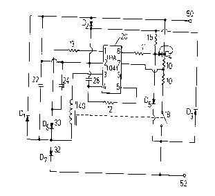
The invention, an embodiment of which is shown in Figures
2 and 3, provides a device suitable for use with wiring of
either polarity. Figure 2 shows a device for fixed load
operation including shunt 10 connected to pin 7 of the
integrated circuit 20 and Figure 3 shows pin 7 disconnected
for variable load operation. Figure 4 is a simplified diagram
showing only the connections of blocking means to the V+, -VCC
and sensing pins of the integrated circuit 20. Terminals 50
and 52 are shown, replacing terminals X and L of Figure 1.
Terminal 50 may be either positive or negative and
terminal 52 may be either positive or negative without
affecting operation of the device. This is achieved by the
presence of diode bridges Dl, D2, D3, D4, D5 and D7. Diodes D6
and D7 correspond to diodes 30 and 32 in Figure 1 and are so
8 ~ ,f c,~
referenced in Figure 2. Thus, diode D7 carries out a dual
function.
Diodes Dl and D7 connect -VCC of integrated circuit 20 to
respective terminals 50 and 52.
When terminal 50 is connected to the positive battery
terminal of an automobile and terminal 52 is connected to the
load, diode D1 will block positive voltage signal reaching -VCC
pin 1. Positive voltage will, however, reach positive pin 2
through diode D2. In this circumstance, terminal 52 will carry
the load and will be relatively negative, essentially
functioning as a ground. Negative voltage will be blocked
from positive pin 2 by diode D3 but will reach -VCC pin 1 by
diode D7. On start-up, a relative negative voltage will be
received at pin 8 from terminal 52 as is necessary for
operation of integrated circuit 20. Thus, for the
configuration where terminal 50 is positive and 52 is
negative, pin 8 receives the proper signal.
When terminal 50 is connected to the positive battery
terminal, a relative negative voltage will initially be
received at sensing pin 8 irrespective of the presence of
diodes D4 and D5, but it may be seen that diode D5 allows such
relative negative signal to reach pin 8.
When terminal 52 is connected to the positive battery
terminal and terminal 50 carries the load, diode D7 prevents a
positive voltage at -VCC pin 1 while diode D1 does not prevent
a negative voltage as a result of the load functioning as a
ground. Similarly, diode D3 allows positive voltage at
positive pin 2 and negative voltage is blocked through diode
D2 .
When terminal 52 is connected to the positive battery
terminal, the situation at sensing pin 8 is a little more
.,
,. .
complex. Sensing pin 8 requires an initial relative negative
voltage to allow pin 3 (not shown on Figure 4 for simplicity)
to conduct. In this case, the presence and arrangement of
diode D5 blocks the transmission of positive voltage from
terminal 52 to pin 8. Special measures are necessary to
ensure the initial relative negative voltage necessary at pin
8. As in the prior configuration, this may be provided by
means of resistor 15. Positive signal from 52 is transmitted
by D3 but, due to resistor 15, relative negative signal is
presented at pin 8. Thus pin 3 conducts with resultant
closing of relay contacts 18, and pin 8 is made positive
through resistor 15 as the positive signal no longer has
access to ground. The sensing pin 8 thus operates normally.
The values for the various resistors 11, 15, 12 and 13 is
a matter of choice to achieve suitable voltages at the
respective pins of the integrated circuit chip 20 and across
the various capacitors. This choice will be within the skills
of a person skilled in the art and will vary with the
circuitry employed.
It may, however, be noted that a device according to the
invention may be made suitable for use with 12-volt batteries,
as are common in automobiles, and may be readily adapted to
use with a twenty-four volt system by the provision of a
suitable resistor 15 in the circuitry. The provision of such
a resistor is possible whichever of terminals 50 or 52 is the
battery terminal.
It is also worth noting that some automobiles are wired
utilizing a positive earth from the battery. A device
according to the invention may readily be adapted for use in
such wiring.