Note : Les descriptions sont présentées dans la langue officielle dans laquelle elles ont été soumises.
203~
A SOLID STATE TELEPHONE LINE CIRCUIT
CROSS REFERENCE TO RELATED APPLICATIONS
Cross Reference is made to the related Canadian
Patent Applications entitled: "A High Voltage Subscriber
Line Interface Circuit," (Attorney Docket 89-1-034), ~A
Circuit For Synthesizing An Impedance Across The Tip And
Ring Leads Of A Telephone Line Circuit, N (Attorney Docket
89-1-035), ~A Tip-Ring Short Detector and Power Shut-Down
Circuit For A Telephone Line Circuit,~ (Attorney Docket
89-1-036), nA Thermal Protection Circuit For An
Integrated Circuit Subscriber Line Interface," (Attorney -~
Docket 89-1-037), "A Thermal Protection Arrangement For
An Integrated Circuit Subscriber Line Interface,"
(Attorney Docket 89-1-038), "A Control Circuit For A
Solid State Telephone Line Circuit," (Attorney Docket
89-1-039), and "A Ring Trip Detector For A Solid State ~ -
Telephone ~ine Circuit, N (Attorney Docket 89-1-040) filed
on the same date, and by the same assignee as this
Application. ;
BACKGROUND OF THE INVENTION
1. Field of the Invention
The present invention relates to the field of
telecommunications and, more particularly, to a solid
state telephone line circuit that provides an interface
between a subscriber station apparatus and a telephone
switching network.
I 2. Description of the Prior Art
Telephone line circuits are customarily found in the
telephone switching system or central office of a
telecommunications network. The telephone line circuit
interfaces the central office, to a telephone or
l ~ubscriber station, found at a location remote from the
central office. The telephone line circuit functions to
supply power or battery feed to the subscriber station
... :: . :: ,
'.:
. .
2~3~0
via a two wire transmission line or subscriber loop and
to couple the intelligence or voice signal to and from
the telephone switching system.
In many presently known telephone line circuits the
battery feed unction has been performed by using a
passive, highly balanced, split winding transformer
and/or inductors which carry up to 12Oma dc. This
passive circuit has a wide dynamic range, passing noise-
free differential signals while not overloading with the
60Hz longitudinal induced currents. The line circuit
jus~ described, feeds dc current to the suhscriber loop
and also provides the voice path for coupling the voice
signal between the subscriber station and the central
office. The electromagnetic components of passive line
circuits are normally bulky and heavy and consume large
amounts of power for short subscriber loop lengths where
the current fed to the subscxiber station is more than
necessary for e~ualization. Active line-feed circuits
can be less bulky and require lower total power, but
meeting dynamic range and precision balance requirements
dictates an overly complex circuit design.
Recently, solid state replacements for the
electromagnetic components of the aforementioned line
circuits have been developed. Devices such as high
voltage bipolar transistors and other specialized
integrated circuits are being designed to replace the
heavy and bulky components of the electromagnetic line
aircuit. Such a device is described in the IEEE JOURNAL
OF SOLID-STATE_CIRCUITS, VOL. SC-16, NO. 4, August 1981,
entitled, nA High-Voltage IC for a Transformerless Trunk
and Subscriber Line Interface.n These smaller and
lighter components allow the manufacture of telephone
switching systems having more line circuits per circuit
card as well as decreasing the physical size of the
s~itching s~stem.
However, presently known solid state line circuits,
still suffer from deficiencies in meeting good
- :
,
~ . . .
.
. . .
:. - . : :
2 0 3 ~
transmission perfor~ance specifications. Thess
defici~ncies manifest themselves in poor longitudinal
balance and poor longitudinal current susceptibility,
which cause the circuit to fail or to become noisy.
Other problems presently encounterad are excessive power
dissipation at short loops that consume prodigious
amounts of central office power and 2 wire input
impedance circuits that are complex and that exhibit poor
return loss.
Accordingly, it is an object of the present
invention to provide a new and more effective solid state
telephone line circuit that will effectively and
efficiently couple a subscribers line station to a
telephone switching system. ~ ~
':
DISCLOSURE OF THE INVENTION ~. -
The above and other objects, advantages, and
capabilities are realized in a solid state telephone line
circuit which is connected via the tip and ring leads of
the subscriber loop to a subscriber station. The solid
state telephone line circuit is further connected via a
Pulse Code Modulation (PCM) bus to a central office
switching system. The solid state telephone line circuit
of the present invention includes an interface circuit,
having a voltage to current converter, connected to the
tip and the ring leads of the subscriber loop. The
current converter is arranged to convert feed voltage
from a central office battery to loop feed current on the
subscriber loop.
The interface circuit further includes a sensing
network connected to the tip and the ring leads for
sensing the voltage dropped across the subscriber loop,
and a differential amplifier circuit connected to the
sensing network. The differential amplifier circuit is
disposed to develop an output voltage that is
proportional to the voltage sensed by the sensing
network.
--3--
". ~ ' - ' ` '
. .
: ' . . - :~ . . . .
2 ~
The solid state telephone line circuit of the
present invention further includes a control circuit,
having a loop current shaping circuit connected to the
differential amplifier circuit. The loop current shaping
circuit is arranged to receive the output voltage
developed by the differential amplifier circuit and
develop and apply to the current converter a control
voltage. The control voltage allows the current
converter to apply feed current to the subscriber loop
that is proportional to loop resistance.
A PCM conversion circuit is also included that is
cormected to the PCM bus. The PCM conversion circuit
converts PCM encoded speech signals received on the PCM
bus from the switching system, into analog speech signals
for transmission to the subscriber station.
Alternatively, the PCM conversion circuit converts analog
speech signals received from the subscriber station to
PCM encoded speech signal for transmission on the PCM bus
to the switching system.
A receive voice path through the solid state
telephone line circuit transmits speech signals from the
PCM bus to the subscriber station. The receive voice
path includes a receive coupling networX, connecting the
PCM conversion circuit to a summing amplifier on the
interface circuit. The output of the summing amplifier
' is applied to the voltage to current converter were the
receive analog voice signals are superimposed on the feed
current and appear as a balanced differential signal on
the tip and ring leads of the subscriber loop.
A transmit voice path through the solid state
telephone line circuit transmits speech signals from the
subscriber station to the PCM bus. Analog speech signals
from the subscriber station appear as differential speech
signals on the tip and ring leads of the subscriber loop.
The analog speech ~ignals are picked up by the sensing
network and fed to the differential amplifier circuit.
The differential amplifier circuit converts the
. .
.
::~ . .. ` ~ ` , '' , ,
. : . .
: . . . .
:
,
2~3~ ~ 8~
differential speech signals into single ended analog
speech signals with a dc offset. The analog speech
signals output from the dif~erential amplifier circuit
are connected to a transmit coupling network where the dc
offset is removed and the resultant speech signals are
applied to an amplifier circuit on the control circuit.
There, the signals are amplified before being routed to
the PCM conversion circuit. The transmit speech signals -
are then converted to PCM encoded speech signals and
coupled to the PCM bus.
BRIEF DESCRIPTION OF THE DRAWINGS
A better understanding of the invention may be had
from the consideration of the following detailed
description taken in conjunction with the accompanying
drawings in which:
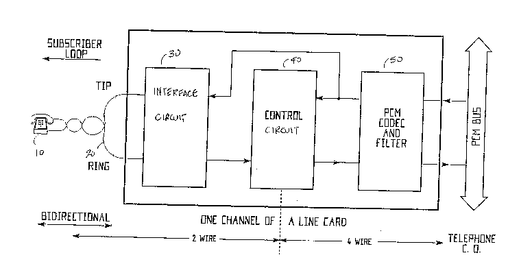
Figure 1 is a broad level block diagram of the solid
state telephone line circuit, in accordance with the
present invention.
Figure 2 is a detailed block diagram of the solid
state telephone line circuit, in accordance with the
present invention.
Figure 3 is graphical representation of the feed
current charaateristics of the solid state telephone line
circuit, in accordance with the present invention.
DESCRIPTION OF A PREFERRED EMBODIMENT
Directing attention ~irst to Figure 1, a broad level
block diagram of the solid state telephone line circuit
of the present invention is shown. The line circuit is
shown driving a subscriber station or telephone 10, via a
subscriber loop 20. The subscriber loop 20 is comprised
of a twisted two wire (2W) loop pair having a tip and a
ring lead. The 2W loop is connected from the subscriber
station 10 to an interface circuit 30. The interface
circuit 30 feeds a -48 V dc voltage to the subscriber
loop across the tip and ring leads from a central office
'
.
203~ 18~
battery (not shown). The interface circuit 30 further
functions to superimpose a voice signal on the dc feed
voltage and also feed ringing current to subscriber loop
20 for signalling. The Interface circuit 30 further
functions to provide the 2W to 4W (four wire) hybrid
function of splitting the balanced signal on the tip and
ring leads into separate transmit and receive paths that
are ground referenced.
The control circuit 40 works in conjunction with the
interface circuit 30 to provide the dc loop current
shaping and the line balance impedance portion of the 2W
to 4W hybrid function. The control circuit 40 further
controls various detection functions, such as, ring trip
detection and loop sense detection, as well as, providing
a logic interface to the central controller of the
central office switching system.
Most modern digital telephone switching systems use
Pulse Coded Modulation (PCM) digital data to convey voice
traffic through the central office switching system.
Therefore, some method of signal translation is required
; to convert the analog voice signals received by the
interface circuit 30 to PCM digital data. This is
typically accomplished by a PCM codec and filter circuit
such as shown at 50. These devices are commercially
available as a so called CODEC/FILTER COMBO~ from various
manufacturers. Such as the TP30XX family of COMBO~
devices manufactured by the National Semiconductor
Company. Analog voice data from subscriber station 10 is
processed by the PCM codec 50 and applied to the PCM bus
of the central office switching system for transmission
to its destination. Similarly, the codec 50 receives PCM
data from the switching system and converts the PCM data
into analog signals which are superimposed on the dc feed
voltage of the subscriber loop 20.
The three solid state circuits 30, 40 and 50 just
described, in combination embody a complete line circuit
.. . . .
. ...
-, . .
. ~ , ~ ,. - ..
. . .
- 2~31~
adapted to connect a single subscriber station to a
central office switch. '!
Referring now to Figure 2, a more detailed
explanation of the functions of the circuits shown in
Figure 1, in accordance with the present invention, will
now be given. The interface circuit 30 shown in Figure
2, is constructed as a bipolar integrated circuit. All
signals requiring high voltages and currents are
interfaced by this device. With the addition of a few
external discrete components a complete transformerless
line circuit can be constructed.
Battery feed voltage VB and current is passed to
interface circuit 30 via transistors 301-304. The
transistors 301-304 are under control of the interface
circuit 30 and electrically should be viewed as though
they were integrated with circuit 30. Due to current and
heat dissipation requirements the transistors 301-304 are ~ -
located external to circuit 30. Current on either the
tip or ring lead of the subscriber loop 20 is sensed by a
network of parallel resistors 305 and 306 whose value is
approximately 50.0 ohms net on each side of the loop 20.
The voltage drop across each resistor 305 and 306 is fed
back to a tip drive and a ring drive amplifier 307 and
308, respectively. A phase splitter amplifier 309,
couples input voltage SUMB to the tip drive amplifier 307
and the ring drive amplifier 308 and together with the
feedback voltage from resistors 305 and 306 create a
voltage to current converter. Input voltage SUMB
controls the loop feed current, such that, a given
voltage at SUMB results in a given current in the
subscriber loop 20 flowing from the tip lead to the ring
lead. The feed circuit of the present invention is
designed to provide a typical gain of 20mA/Volt at SUMB.
It should be noted that the current feed in
subscriber loop 20 is not a constant current, as the
aforementioned discussion may imply. Rather, the current
is shaped to provide sufficient variation of current
~ " , .
:: , :,. - . : . :
. ~, ' : ' ' .' ' : ' ' -
-~ " ~ , : -
',; '.': ' ` ' . -
: ~
8 ~
versus loop resistance to ensure ef f icient power usage.
This is accomplished by providing a feedback loop between
the interface circuit 30 and a loop current shaping
circuit 401, found on control circuit 40. As loop
resistance becomes less than 2K Ohm, a resistor network
comprising resistors 310-311 apply the voltage drop
sensed across subscriber loop 20 to a XMT Differential
amplifier 314. A voltage that is proportional to the
voltage sensed by resistors 310-311 then appears at XMTB
of circuit 30. The voltage at XMTB is fed to a loop
current shaping circuit 401, where it is properly shaped
and output at the DLC node of circuit 40. This shaped
voltage is fed back to the phase splitter amplifier 309
as the SUMB input voltage.
The current shaping just described generates the
feed current characteristics shown on Figure 3. The
smoothly decreasing current with loop resistance, allows
power savings at short loops, while still providing
sufficient variation of current versus loop resistance to
ensure proper transmit levels from the subscriber
! station. As the total external resistance becomes
greater than 2K Ohms, the battery feed reverts to a
constant voltage feeding scheme.
Input impedance of the line circuit of the present
invention is synthesized by the combination of an
impedance network comprising, capacitor 402 and resistors
~03 and 404 for the fixed value of the feed resistance
used in the design. As mentioned earlier, the feed
resistance value for the line circuit is 50.0 Ohms net on
each side of the subscriber loop 20. An analog
represen~ation of the tip and ring difference voltage
developed by the XMT differential amplifier 314 is output
to node XMTA of the interface circuit 30. The voltage at
node XMTA is coupled to the impedance network and fed to
the AC summing node SUMA of circuit 30. The overall
feedback generates an input impedance, as seen from the
tip and ring leads, that is a scaled (in magnitude)
~ . .
-
~'`'` 2~1 L~
version of th~ impedance network. The impedance network
of the present invention yields an equivalent 900 Ohms in
series with 2.16uF impedance.
In conventional 200/200 ohm inductive battery feed
line circuits, the impedance to ground at either the tip
or ring leads is essentially half the f~ed resistance.
In the present invention, feed resistance is synthesized
by feedback techniques, so that longitudinal impedance is
not related to feed resistance. A common mode voltage,
(VTIP+VRING)/2, is developed between a voltage divider
network comprising resistors 312 and 313 and input to
interface circuit 30 at CM. This applied voltage
together with the tip drive amp 307 and ring drive amp
308 keep the voltage at AT and AR on circuit 30 constant
when longitudinal currents, such as 60 Hz power line
induction currents, that may be induced on the tip and
ring leads. Interface circuit 30 sources or sinks the
longitudinal currents as required up to 9mA per lead.
Since the voltage at AR or AT appear as a virtual AC
ground to longitudinal signals, the impedance to ground
is simply the series resistance of resistors 305 and 317
on the tip lead and the series resistance of resistors
318 and 306 on the ring lead, each approximately 75 Ohms
per leg.
With renewed reference to Figure 2, the voice paths
followed by the speech signals through the line ci~cuit
of the present invention will now be described. The
receive voice path, analogous to the path used to
transmit speech signals to the receiver of the subscriber
station 10 will be explained first. PCM representations
of speech signals are applied to the PCM codec and filter
50 at DR via lead PCMR from the PCM bus of the central
office switching system. The PCM signals are converted
to analog signals by a digital to analog converter (not
shown) internal to the PCM codec 50. The analog speech
signals are then output from the PCM codec and filter 50
at VFRO and are capacitively coupled by capacitor 407 to
.. . .
" '' . '
:
~' ~ : ,.
.
~ ~ 3 ~
resistor 408. Resistor 408 terminates at node SUMA of
interface circuit 30. The SUMA node is a virtual ground
for AC summing amplifier 315 and is also arranged to
perform signal summation of the receive signal and the
transmit signal output from XMTA. The summation just
described is also used in the synthesis of the line
circuits input impedance, as explained earlier. The
speech signals are output from AC summing amplifier 315
and connected to phase splitting amp 309 where they are
coupled to the subscriber line via the tip and ring drive
amplifiers 307 and 308. The speech signals thus appear
as a balanced differential signal on the tip and ring
leads of the subscriber line 20. The ratio of resistor
40~ ov~r resistor 408 sets the initial gain for the
output of AC summing amplifier 315.
The transmit voice path, analogous to the path used
to transmit speech signals from the transmitter of the
subscriber station will be explained now. The
differential tip/ring speech signals transmitted from the
subscriber station 10 over the subscribers line 20, are
initially coupled to the interface 30 via resistors 310
and 311. The received differential speech signals are
applied to XMT differential amplifier 314 which converts
the speech signals to a single ended signal that appears
at the XMTA node of interface circuit 30. The speech
signals at the XMTA node are the transmit speech signals
with a dc offset. The transmit speech signals are then
coupled to resistor 403 via capacitor 402. Capacitor 402
removes the dc offset and only the ac speech signals
remain across resistor 403. The speech signals at
resistor 403 are fed to the XMTA node of control circuit
40 were a high impedance amplifier 408 provides gain.
The amplified transmit speech signals then have a
~reflection replicaN of the receive side signal
subtracted from them and the net signal is output from
node XMT to the +VXI input of the PCM codec filter 50.
The speech signals are then converted into PCM digital
--10--
... .
:~ ~: , ?
- .
20311~
data and output to the central office switch via node DX
and the PCMX lead.
The line circuit of the present invention is
arranged to provide either loaded or non-loaded line
balance, under software control. Switched capacitor
filter 405 o~ ~he control circuit 40, includes three
switched capacitor filters, one for non-loaded lines and
one for loaded lines and one for 9:2 loaded lines. The
capacitor filters appear between the receive side speech
signal at RCV of circuit 40, and AC summing amplifier
315. The switched capacitor filter 405 combines the
; filtered signal with the transmit speech signal from
XMTA. The filters 405 have a response which models the
gain phase of the selected (loaded, non~loaded, or 9:2
loaded) line and the interface circuit 30 plus external
components. The signal output from the filters 405 is
out of phase with the transmit speech signal. The net
result is that the "echoN from the receive side voice
path is canceled on the transmit side voice path before
it is output to the transmit side listener.
Loop sensing, is the detection of on/off hook status
of the subscriber and the replication of dial pulsing for
dial pulsing equipped subscriber stations. All loop
sensing detection in the present invention occurs within
the control circuit 40. This detection is accomplished
by sensing an analog representation of the loop voltage
~ and comparing the analog representation to a fixed
; threshold with a comparator. This is accomplished in the
Pollowing manner. As explained earlier for the battery
faed function of the present invention, a voltage that is
proportional to the voltage across the subscribers line
20 normally appears at node XMTB of control circuit 40.
This voltage is processed by loop current shaping circuit
401 and an output signal which is proportional to loop
current is generated at node DLC. This signal is passed
to loop sense circuit 409 and is compared to a 750mV
reference voltage. The output of the loop sense circuit
-11-
.. . ..
-
,
:-
. ~ . , :
~3~ ~3i~
409 iS connected to logic circuit 410. When, forexample, a ring trip occurs a latch internal to logic
circuit 410 is set and its data read by the switching
system central controller via control bus 412. Capacitor
413 together with resistance internal to loop sense
circuit 409 form a symmetrical integrator. This
integrator is disposed to provide "~IT" protection by
blocking transient "off hookn or "on hook~ pulses of less
than 12 msec from being detected by the loop sense
circuit 409.
High voltage transients and power cross protection
is afforded to the line circuit of the present invention
by the inclusion of a diode rectifying bridge circuit
201. The bridge circuit 201 directs positive voltage
transients to ground and the negative voltage transients
to a special transient protection semiconductor 202.
Device 202 acts as a SCR type device ~ith an internal
gate triggered by excess voltage in the range of 85 Volts
that shorts the transient to ground for its duration.
Power cross protection is afforded to the line circuit
via 900 mA lighting surge fuses 203 and 204 that are
placed in series with each tip and ring conductor
respectively.
The solid state telephone line circuit just
described can be manufactured as a single compact hybrid
circuit using any of the presently known thin film
techniques u~ed to build microcircuits. Further,
interface circuit 30 and control circuit 40 can each be
manufactured as large scale integrated circuits suitable
for mounting on the hybrid assembly. The hybrid assembly
can thus provide the capabilities of a line circuit which
in the past occupied a complete circuit card to a line
circuit having a greater functional capability and
occupying one sixteenth the same space. The solid state
telephone line circuit of the present invention also
benefits from the increased reliability inherent in solid
-12-
~' ' .
. ~, .
.
. - .
:: `
: ~ , : ' , ,
203~
state construction as well the economies in labor cost
and manufacture which are enjoyed by solid state devices.
It will be obvious to those skilled in the art that
numerous modifications to the present invention can be
made without departing from the scope of the invention as
defined by the appended claims. In this context, it
should be recognized that the essence of the invention
resides in a solid state telephone line circuit having
the advantages and capabilities described herein.
-13-
.
.
::-:: . .