Note : Les descriptions sont présentées dans la langue officielle dans laquelle elles ont été soumises.
20317~3
LINE UNIT INTERFACE CIRCUIT
BACKGROUND OF THE INVENTION
Field of the Invention
The present invention relates to digital loop
carrier (DLC) systems and, more particularly, to a line
unit interface circuit for interfacing line units with
common equipment in a digital loop carrier line shelf.
Description of the Prior Art
The Synchronous Optical Network (SONET) standard
(American National Standards Institute Standard Tl.105-
1988 entitled "Digital Hierarchy Optical Interface
Rates and Formats Specification") which is being
adopted within the United States and elsewhere defines
the standard for the transfer of information by means
of optical fiber. According to the SONET standard, an
optical carrier level (such as OCl, OC3, OC12 and OC48)
signal is a signal that results from an optical
conversion of a synchronous transport signal (STS)
operating at the same transfer rate. An STSl level
signal is defined as the basic building block signal,
with a high-speed transfer rate of 51.840 Mb/s, and is
equated to an OCl level optical signal. With high-
~'
2~3~3
speed transfer rates there is a need for multiplexingand demultiplexing information associated with lower-
speed telephony standards to and from the high-speed
transmission lines. Examples of such lower-speed
standards include the digital signal standard, or DSX
standard (where 'X' is an integer, such as 0, 1, 2 and
3). The DSX standard is commonly used in telephony
with DSO directed to subscriber level signals that
operate at 64 Kb/s, DSl directed to lines operating a
1.544 Mb/s, DS2 operating at 6. 312 Mb/s, and DS3
operating at 44.736 Mb/s.
In order to access the high-speed transmission
lines, network elements are required for transferring
and grooming, i.e., segregating, subscriber information
channels between the lower-speed transmission lines and
the higher-speed transmission lines. These network
elements may take on several different forms for
providing transfer of information between various
standard transmission rates. In order to take
advantage of the wider bandwidth available on the high-
speed lines for various applications such as data
transfer, a means was required to combine DSO channels
to provide wider band facilities.
2031793
65993-204
A famlly of access products has been developed by the
Asslgnee of the present invention. These access products allow
slower transmission lines to access the higher-speed optical
transmission systems. These access products use an internal
multi-link serial bus (SBI) operating at a rate of 4.096 Mb/s to
transport information, signalling and processor commands. U.S.
Patent No. 5,060,229, entitled "Serial Transport Frame Format
Method", and assigned to the assignee of the present
applicatlon, describes this unique serial bus. Two access
products are also described in the aforementioned patent, said
access products being a Terminal Multiplexer, adapted to
interface a high-speed carrier with DS1 level transmission lines
for reception and transmission of high-speed signals in one
direction only. An Add/Drop Multiplexer (ADM) is also described
in the aforementioned patent and is designed to interface a
high-speed carrier to DS1 level transmission lines for reception
and transmission in each of two directions.
DES~ ON OF THE DRAWINGS
Figure 1 is a block diagram illustrating the
environment in which the present invention is used as compared
to that of the prior art.
Figure 2 is a block diagram of a line shelf in which
the present invention ls used.
Figure 3 is an elevational view showing the structural
configuration of a line shelf in which the present invention is
utilized.
203179~
- 65993-204
Figure 4 is a block diagram of the present invention.
Figures 5A, B and C show signal timing relationships
used in the present invention.
Figure 6 illustrates a high-level schematic diagram of
the present invention.
Figure 7 shows a schematic diagram of the time slot
decoder of Figure 4.
Figure 8 shows a schematic diagram of the flywheel
circuit of Figure 7.
Figure 9 shows a schematic diagram of the variable shift
register of Figure 8.
Figure 1 illustrates the use of access products in a
telephone transmission system. Two high-speed feeder lines 10 and
12 are shown as being at the optical OC1
-` 20317 93
65993-204
level and the electrlcal STS1 level respectively. Both of these
feeder lines operate at 51.84 Mb/s. An add/drop multiplexer 14,
as described in the aforementioned patent, connects either
feeder line 10 or 12 to a DS1 level transmission line 16
operatlng at 1.544 Mb/s. In order to extract lndividual DS0
channels from the DS1 line, a separate network element 15
usually referred to as a DLC was required as an interface
between the DS0 level and the DS1 level. In a commercial
installation several DLCs would be used with each add/drop
multlplexer. Thus two separate network elements 14 and 15 were
requlred in order for individual lines at the DS0 level to
access an optical OCl level transmission line, and in most cases
several DLCs were used wlth one multlplexer.
The need for a DS1 level transmisslon line between the
ADM 14 and the DLC 15 severely limited the control
communications that could take place between the two network
elements. The use of two separate network elements inherently
reduced reliability, since all control lnformatlon had to be
conveyed over a slngle DS1 line. Control information in the
form of signaling could be conveyed only to a limited extent
using the robbed bit signallng technlque and clear channel
2031793
communication was not available. A means did not exist
for the microprocessors in each element to communicate
with each other unless a separate DSO channel was
dedicated to this purpose, removing this particular DSO
channel from the pool of DSO channels available to
carry subscriber traffic.
The DLCs are generally adapted to accept a
plurality of line units servicing one or more DSO
channels each. The line units are connected to a TDM
bus with the line signals being multiplexed onto the
bus at specified time slots, each line unit having
predetermined time slots for inserting and extracting
data to and from the bus for each of its channels. The
line unit would be strobed to be activated during the
time slots to which it is assigned. A plurality of
back plane connections were required to provide a
strobe signal to each line card. Thus, the system was
limited to a pre-set number of line cards that could be
handled by the system, and the assignment of the time
slots to the line cards was fixed.
Control of the system was limited, since the
system controller did not have access to the data
contained within each time slot, including signaling
information pertaining to the time slots.
G
A
203I 793
With the advent of many different types of
telecommuni-cations service, various signaling schemes
have been devised which are not compatible with each
other. Signaling translation between equipment using
one signaling scheme and equipment using another
signaling scheme was required and the use of special
signaling translation circuits for each different type
of service had to be developed. Thus, the free
interchange of line cards was restricted, due to the
need to first provide for the required signaling
translation.
Modern telecommunications systems must provide for
high-speed wide bandwidth data communications
facilities which cannot be serviced by individual DSO
level lines. Thus, higher speed DS1 lines had to be
provided to handle individual customer requirements
when they exceeded the capability of a DSO line.
Thus, it was apparent that the flexibility
demanded by modern telephone communications systems was
not being efficiently handled by the prior art
interfaces between high-speed feeder lines and DSO
level subscriber lines. There was clearly a need for a
more efficient way of providing access to high-speed
transmission lines by individual DSO subscriber lines.
2031793
65993-204
SUMMARY OF THE INVENTION
The present invention contemplates a circuit for
interfacing line units serving one or more subscriber lines with
common equipment in a line shelf of a DLC access product and, more
particularly, to a circuit for interfacing DSO subscriber line
circuits with a time slot access device (TSA) as described in U.S.
Patent No. 5,088,089, entitled "Apparatus For Programmably
Accessing and Assigning Time Slots In A Time Division Multiplexed
Communication System", and assigned to the Assignee hereof.
U.S. Patent No. 5,161,152, entitled ~High-Speed
Synchronous Transmission Line Access Terminal", and assigned to
the Assignee hereof. Said patent describes a single network
element which will interface a high-speed feeder transmission line
10 or 12, with a lower speed DSl line 16 and DSO subscriber lines
20, as shown in Figure 1. The network element is an access
terminal 22 having a core module 24 connected to either feeder
line 10 or 12 and having ports connected to DSl line 16 and to an
access module 26 having ports connected to DSO lines 20.
~ 8
- `` 2031793
65993-204
The access module 26 may comprise a plurality of
individual line shelves, each of which may further accommodate a
plurality of line units for connection to individual subscriber
lines. Each line shelf may accommodate up to 96 subscriber lines,
with the core module 24 accommodating up to seven line shelves,
for a total of 672 subscriber lines, each having access to an
optical fiber carrier OC1 or an STS1 metallic feeder line.
The core module 24 is connected to the line shelves of
the access module 26 by a plurality of SBIs, as disclosed in the
aforementioned U.S. Patent No. 5,060,229. The SBIs facilitate an
embedded control technique for communicating control messages over
channel 31, called the VI channel. This embedded control
technique is described in U.S. Patent No. 5,027,349, entitled
~Embedded Control Technique for Distributed Control Systems",
assigned to the Assignee of the present application. The SBI
using the VI channel allows the DSO level signals to be tightly
coupled to the high-speed OC1 or
- 2031793
STS1 feeder lines. The technique allows for clear
channel transmission by eliminating the need for the
robbed bit technique and also provides for processor-to-
processor communication between modules. The
flexibility of the SBI arrangement facilitates
signaling processing, provisioning and maintenance
functions.
A pair of processors are used in both the core and
in the line shelves to provide a host of advantages
which will become apparent. One advantage is the
unique flexibility provided in grooming DS0 channels
and the ability to combine them to provide wider
bandwidth capability to service future communications
needs such as ISDN. Another advantage of using a line
shelf processor (LSP) lies in its adaptability to
future enhancements and reconfigurations by merely
effecting a software change.
The heart of the line shelf is a line shelf access
unit (LSA) which interfaces the line units (LUs) and
the SBIs. Each LSA includes a pair of time slot access
devices (TSAs) which function to collect and distribute
pulse code modulated (PCM) signals, signaling,
provisioning and configuration data between the SBIs,
the LUs and the LSPs. The TSA provides the LSPs with
direct access to the data contained within a particular
/~
,~
- 2031793
time slot. This data may contain speech information,
signaling and other control information, thereby
providing the LSPs with heretofore unavailable control
capabilities.
The TSA also facilitates a time slot assignment
feature which is controlled by the LSP to provide
assignment of any particular time slot to any
subscriber line on any LU, or a plurality of time slots
to a single subscriber line to provide broad band
capability.
The TSA also provides for signaling translation
between the signaling scheme used in the particular LUs
and the signaling scheme used for signals received on
the SBI. The signaling translation function is
accomplished via a downloadable translation table,
which is written into RAM contained in the TSA unit by
the LSP.
The TSA, as previously mentioned, provides a
plurality of signals on a line unit interface bus which
is connected to the various line units. The line unit
interface bus carries two clock lines; eight serial
data lines for the transmission and reception of PCM
data, signaling, configuration data and provisioning
data; and two data lines for transmitting and receiving
inventory data stored on the line units.
- 2031793
The line unit interface circuit (LUC) of the
present invention performs all of the functions
necessary to interface an LU to the common equipment
(TSA) via the line unit interface bus. These functions
include generation of the necessary framing and timing
signals for the line units from two clock signals
received from the TSA, the receipt and transmission of
signaling and provisioning data, and access to
inventory data stored on the line units. A major
function of the LUC is to decode configuration data
received from the TSA, including offset information, to
ascertain the time slots on a TDM transmission line
assigned to the subscriber channels serviced by the
line units, and to further decode the offset
information when a difference between the receive and
transmit time slots is required.
When a configuration code received on the line
unit interface bus matches a fixed code provided to the
LUC by back plane straps connected to identification
pins, access to an RX and a TX time slot on the TDM bus
is provided. Also provided is a bit-mapped output port
decoded from signaling data received on the line unit
interface bus to drive various line circuit relays,
alarms and indicators. A chip select signal and clock
for the inventory storage is also generated.
20~1793 65993-204
The LUC also accepts signaling lnputs from detector
sections of the llne unlt and encodes these lnputs onto a serial
signaling output bus on the line unit interface bus and provides
framing and sync slgnals for the llne unlt codecs servlcing each
subscriber llne.
The decoding circuitry for decodlng the configuration
data lncludes a unlque flywheel clrcult for preventing the
erroneous assignment of time slots resultlng from nolse or false
signals received on the llne unlt interface bus from the TSA.
The offset data ls provlded to a unlque variable shift register
for controlling the number of tlme slots between the tlme a line
unlt ls activated for reception and for transmlsslon.
The lnventlon may be summarlzed, accordlng to a broad
aspect, as an lnterface circult for use on a llne unit ln a line
shelf of a digital loop carrler for lnterfaclng wlth a bus
connected to a llne shelf common equlpment, sald bus conveylng
tlme slot conflguratlon data for a plurallty of line unlts, said
interface clrcuit comprislng means, connected to sald bus, for
recelvlng and decoding sald tlme slot conflguratlon data and
means for actlvatlng the llne unlt ln accordance wlth the
decoded tlme slot conflguratlon data.
A prlmary ob~ectlve of the present lnvention is to
provlde an lnterface between llne unlts of a llne shelf and
common equlpment of the llne shelf.
Another ob~ectlve of the present lnventlon ls to
provlde for the decodlng of tlme slot asslgnment codes provlded
as conflguratlon data.
--
2031793
65993-204
Another objective of the present invention is to provide
a safety feature to prevent the erroneous assignment of time slots
due to noise or spurious signals.
Another objective of the present invention is to decode
offset data provided with the configuration data to establish a
time delay between activation of the line unit for reception and
transmission.
Another objective of the present invention is to provide
an interface for signaling and provisioning data.
Another objective of the present invention is to detect
a chip select bit in the configuration data and to access
inventory information stored on the line unit.
DETAILED DESCRIPTION OF THE PRESENT INVENTION
Referring to Figure 2, there is shown a block diagram of
a line shelf used in the access module 26. Each line shelf is
arranged with four groups 28 of subscriber lines at the DS0 level.
Each of the groups includes 12 line units (LUs) 30, most LUs are
capable of handling two subscriber lines so that a total of 96
subscriber lines may be handled by a line shelf. A pair of line
shelf access units ~LSAs) 32 are arranged to each service two of
the groups 28 of subscriber lines and function to multiplex the
DS0 channels of these groups to a pair of serial interface buses
(SBIs)
2031793
34, one of which is redundant. Two line shelf
processors (LSPs) 36 are provided to control the LSAs
32, with each processor having sufficient capacity to
control the entire line shelf in the event of failure
of the other processor. Thus, in normal operation both
processors work at less than full capacity. In the
event of a failure, one processor can service the line
shelf with only slightly degraded service. Two power
supplies 38 are also provided, with one being
redundant.
The LSAs 32 are connected to the various LUs 30
via line unit interface buses 40. The line unit
interface buses 40 interface with a line unit interface
circuit (LUC) 42 provided in each of the LUs 30. The
LUCs 42 perform all the functions necessary to access
the line unit interface buses 40 with the LUs 30.
The LUs 30 are plugged into slots in the line
shelf, which includes connectors to the line unit
interface bus 40. The connectors have five pins that
are selectively strapped to provide a five-digit
identification code for the slot and the subscriber
lines on the plugged-in LU. The LSP periodically scans
the various card positions and can detect when a card
is plugged into an identified slot.
-15-
2031793
EEPROMs 50 are provided on each of the pluggable
card units, such as the LUs, LSAs, LSPs and power
supplies. The EEPROMs 50 provide storage for
identification and inventory information about each
card and other programmable data relating to the
circuitry on each card.
The LSAs 32 each include two time slot access
circuits (TSAs) 44 and a clock generator 46. The TSAs
44 are connected to each LSP 36 via LSP buses 48 and
perform most of the functions of the LSAs 32.
The TSAs 44 perform the following functions in the
access terminal 22: reception and transmission of SBI
signals; detection and generation of UNICODE and
performance of required tasks associated with UNICODE;
collection of PCM-formatted information from the LUS
and the LSPs; distribution of PCM information to LUS
and the LSPs; generation of configuration codes to
indicate to the LUs which time slot is available on the
various line unit interface buses 40; generation of a
coded signal provided in channel 30 of each frame
indicating an offset delay between the receive time
slot for a subscriber line and the transmit time slot
for a subscriber line, which delay is dependent upon
delays encountered during initialization of the system;
translation of signaling information between the SBIs
2031733
and the LUs by utilization of RAM-based translation
tables provisioned by the LSP; LSP access in both read
and write modes to all memory and control registers on
the TSA, including access to the time slots of the line
unit interface bus and the SBI; reception and
transmission of inter-module messages on the VI
channel; control of EEPROMs on each plug-in unit; and
the provision of storage for information to be
transmitted to and received from the various elements
connected to the TSA.
Referring to Figure 3, there is shown the
arrangement of a line shelf having four groups of line
units 28, each group consisting of 12 line units
serving 24 separate subscriber lines. Each line unit
is inserted in a designated slot and is connected to
back plane wiring. Line groups A and C on the left
side of the line shelf are identified as being
associated with a line group 0, while the line units of
line groups B and D are on the right side of the shelf
and are associated with a line group 1.
For the LSA 32 of Figure 2 to assign a time slot
on a line unit interface bus (LUIB) 40 to a subscriber
line, a slot address including the slot number of the
line unit 28 serving the subscriber line, the line
group bit (LGB) for the slot and the channel A or B bit
-17-
- 20317g~
for the line unit is sent over an RX configuration bus
(CONR), a line of the LUIB 40, as a coded configuration
word two time slots before the actual time slot to be
assigned. This timing allows the LUC 42 enough time to
decode the configuration word.
Referring to Figure 4, there is shown a block
diagram of the LUC 42. The configuration word from the
CONR bus is received and latched in a shift register
and latch 54 that is part of a time slot decoder 52.
The LUC 42 compares this received slot address to hard-
wired slot address pins (SLADD0-3) from the backplane
and compares the received LGB bit to the LGB bit from
the backplane in a slot comparator 56. Then the LUC
determines which line unit channel A or B the time slot
is being assigned to, and generates an appropriate
timing strobe.
After the CONR data is decoded, the timing strobe
is sent to a flywheel circuit 58 for the appropriate
line unit channel. This circuit reduces the chance of
an intermittent error in the CONR data producing an
incorrect activation strobe to activate an
inappropriate line unit channel. The flywheel circuit
is centered around a 5-bit counter that counts from 0-
31, the number of time slots in a frame. It takes two
frames of a new strobe address to re-sync the 5-bit
-18-
2031793
counter to a new time slot position. When the counter
is in sync, the output will be zero one time slot
before the strobes are produced.
The receive and transmit time slots in the TSA
chip can have an offset of from 0-31 time slots. This
offset is sent as an offset number by the TSA over the
CONR line of LUIB 40 in time slot 30. The offset
number does not change after it is set by the TSA,
unless the TSA re-syncs. An offset register circuit 60
latches the offset number and must receive two offset
numbers of equal value for the register to be updated.
Signaling and provisioning data is processed in
block 61 which includes sub-blocks for handling
received signaling, transmitted signaling and
provisioning data. Signaling data (SIGR) is received
from the LUIB 40 in serial format and is converted to
eight parallel output bits for each channel in a shift
register 62 and latches 80.
Transmit signaling is generated by detectors in
the line units which provide four detector inputs DETA3-
O and DETB3-0 to the LUC for each channel. These
parallel inputs are converted to serial data by a shift
register 64 and multiplexer 66 and are gated onto the
LUIB 40 by transmit strobes from the time slot decode
circuit 52.
--19--
203I 793
Received provisioning data (PROR) is reconfigured
in logic circuit 68 and then shifted out as
provisioning data (RXSLPRAorB) to subscriber line
interface modules (SLIMs) in the line units.
The EEPROM chip select 69 is controlled by bit 6
of a configuration word received on CONR from the TSA.
Bit 6 is used in logic 70 to generate an EECS output
which is used to activate EEPROM 50 used in storing
inventory control information and provisioning
information.
There are two spare HC type inverters 72 and 74
available that can be used as needed.
The LUC receives and transmits a plurality of
signals that are identified in Table 1. The signals
marked * are active when low.
TABLE 1
Signal Signal Interface
Name Description In/Out Type
VDD1&2 Power Supply +5VDC
VSS1-3 Power Supply Reference GND
POR* Power On Reset Low Input CMOS
FWDIS* Flywheel Disable Low Input CMOS
SLADD3-0 Slot Address 3-0 Input CMOS
LGB Line Group Bit Input CMOS
CLK256 256 KHz Clock Input CMOS
CLK2048 2.048 MHz Clock Input CMOS
SIGR Receive Signaling Input CMOS
SIGT Transmit Signaling Output
CONR Receive Configuration Input CMOS
FSXA&B Frame Sync Transmit A & B Output
FSRA&B Frame Sync Receive A & B Output
-20-
2031793
TABLE 1 (cont.)
TXABS* Transmit A and B Strobe Output
SLCSA&B* SLIM Chip Select A & B Low Output
DETA3-0 Channel A Detectors 3-0 Input CMOS
DETB3-0 Channel B Detectors 3-0 Input CMOS
IVlI Inverter l In Input CMOS
IVlO Inverter 1 Out Output
IV2I Inverter 2 In Input CMOS
IV20 Inverter 2 Out Output
EECS EEPROM Chip Select Output TRI-STATE
EECLK EEPROM Clock Output
EEPROG* EEPROM Program Low Input CMOS
RXCOA&B Receive Control Output A & B Input CMOS
TXCOAB TX Control Output A & B Output
BLEDA*/ Busy Led A/Channel A Rel O Output OPEN-DRAIN
RELAO
FLEDA*/ Fail Led A/Channel A Rel 1 Output OPEN-DRAIN
RELA1
RELA7-2 Channel A Relays 7-2 Output
BLEDB*/ Busy Led B/Channel B Rel O Output OPEN-DRAIN
RELBO
FLEDB*/ Fail Led B/Channel B Rel 1 Output OPEN-DRAIN
RELB1
RELB7-2 Channel B Relays 7-2 Output
RXSLPRA&B Rec SLIM Provisioning A & B Output
ABLED* Auxiliary Busy Led Low Output OPEN-DRAIN
AFLED* Auxiliary Fail Led Low Output OPEN-DRAIN
PROR Receive Provisioning Input CMOS
DPROR Delayed Rec Provisioning Output
The following is a brief functional description of
the signals listed in Table 1:
POR* Power On Reset low. This input inhibits
strobes to the line unit channel and resets
part of the circuits in the LUC.
FWDIS* Flywheel DISable low. This input disables
the flywheel circuit 58.
-21-
20317~
LADD3-0 SLot ADDress 3-0. Bits 3-0 of the slot
address.
LGB Line Group Bit. This bit indicates which
line group the line unit is installed in.
LGB = 0 indicates the left side of the line
shelf; LBB = 1 indicates the right side.
CLK256 CLocK 256 KHz. A 256 KHz clock from the TSA
44 on the LSA 32. Low for the first 4 bits
and high for the second 4 bits, and
corresponding in frequency to the time slot
rate.
CLK2048 CLocK 2.048 MHz. A 2.048 MHz clock from the
TSA 44 on the LSA 32.
SIGR SIGnaling Receive. Signaling data from the
TSA 44 on the LSA 32 at a data rate of 2.048
MHz, 32 time divisions multiplexed, 8 bits
per sample, 8 KHz sample rate.
2031793
SIGT SIGnaling Transmit. Signaling data to the
TSA 44 on the LSA 32 at as data rate of 2.048
MHz, 32 time divisions multiplexed, 8 bits
per sample, 8 KHz sample rate.
CONR CONfiguration Receive. Configuration data
from the TSA 44 on the LSA 32 at a data rate
of 2.048 MHz, 32 time divisions multiplexed,
8 bits per sample, 8 KHz sample rate.
FSXA&B Frame Sync Transmit A & B. Strobes to the
appropriate COMBO or SLIM to indicate the
beginning of transmit time slots. High
active output, CMOS and TTL compatible.
FSRA&B Frame Sync Receive A & B. Activation strobes
to the appropriate COMBO or SLIM to indicate
the beginning of receive time slots. High
active output, CMOS and TTL compatible.
TXABS* Transmit A and B Strobe low. A strobe used
to enable tri-state backplane drivers
(located outside the LUC) during the transmit
time slots of channel A and/or B. Low
active. Output, CMOS and TTL compatible.
-23-
2031793
.
SLCSA&B* SLim Chip Select A & B low. Strobes to the
appropriate SLIM used with CLK2048 to clock
control words in and out of the control
interface. Active low during the receive
channel. Output, CMOS and TTL compatible.
DETA3-0 DETect A 3-0. These four channel A input
signals are converted to serial data and
gated onto a SIGT line of LUIB 40 with
strobes from the time slot decoder 52 during
a transmit time slot. Input, CMOS
compatible.
DETB3-0 DETect B 3-0. These four channel B input
signals are converted to serial data and
gated onto a SIGT line of LUIB 40 with
strobes from the time slot decoder 52 during
a transmit time slot. Input, CMOS
compatible.
IVlI InVerter 1 In. An input to inverter 72.
Input, CMOS compatible.
2031793
IV10 InVerter 1 Out. An output of inverter 72.
Output, CMOS and TTL compatible.
IV2I InVerter 2 In. An input to inverter 74.
Input, CMOS compatible.
IV20 InVerter 2 Out. An output of inverter 74.
Output, CMOS and TTL compatible.
EECS EEprom Chip Select. An EEPROM chip select
signal to activate EEPROM 50 on the line
unit. Output, Tri-state.
EECLK EEprom CLocK. A 256KHz EEPROM clock the same
as CLK256. Output, CMOS and TTL compatible.
EPROG* EEprom PROGram LOW. This signal tri-states
the EECS output so an external device can
program the EEPROM 50. This signal is only
provided during factory testing and does not
come from the LUIB. Output, CMOS and TTL
compatible.
- 2031793
RXCOA&B Receive Control word Output A & B. The LUC
clocks in control output words from the line
unit channels A and B during the RX time
slots. This byte is stored until the TX time
slots when it is clocked out of the TXCOAB
output. Input, CMOS compatible.
TXCOAB Transmit Control word Output A & B. The
bytes that were clocked into the LUC on
inputs RXCOA and RXCOB during the receive
time slots of channels A and B are clocked
out of this pin during the transmit time
slots. Output, CMOS and TTL compatible.
RELA7-2 RELay A 7-2. These outputs are normally used
to drive relay drivers. Output, CMOS and TTL
compatible.
FLEDA/
RELA1 Failed LED A/RELay A 1. This output is used
to drive the card failed LED or with a pullup
resistor can be used as a normal output.
Output, Open-drain.
BLEDA/
-26-
2031793
RELA0 Busy LED A/RELay A 0. This output is used to
drive the card busy LED or with a pullup
resistor can be used as a normal output.
Output, open-drain.
ELB7-2 RELay B 7-2. These outputs are normally used
to drive relay drivers. Output, CMOS and TTL
compatible.
LEDB/
RELB1 Failed LED B/RELay B 1. This output is used
to drive the card failed LED or with a pullup
resistor can be used as a normal output.
Output, open-drain.
BLEDB/
RELB0 Busy LED B/RELay B 0. This output is used to
drive the card failed LED or with a pullup
resistor can be used as a normal output.
Output, open-drain.
XSLPRA&B Receive SLim PRovisioning A & B data. This
data is used to provision a National SLIM
chip used for a subscriber line interface.
Output, CMOS and TTL compatible.
-27-
`- 2031793
ABLED* Auxiliary Busy LED. Output to drive the busy
LED on a TACC card. Output, open-drain.
AFLED* Auxiliary Failed LED. Output to drive the
failed LED on the TACC card. Output, open-
drain.
PROR PROvisioning Receive data. Data from the TSA
44 on the LSA 32 at a data rate of 2.048Mb/s,
32 time divisions multiplexed, 8 bits per
sample, 8Kb/s sample rate. Input, CMOS
compatible.
DPROR Delayed PROvisioning Receive data. This is
the same as PROR, except that it is delayed
1/2 bit time. Output, CMOS and TTL
compatible.
The input and output timing for the LUC is shown
in Figures 5A to 5C. The data is transmitted on the
LUIB 40 in 125us frames, each having 32 time slots.
Eight data lines are illustrated in Figure 5A,
representing the receive and transmit lines for PCM
data (this data is connected directly to the line units
-28-
2031793
and not through the LUC), signaling data, provisioning
data and configuration data. Each time slot is further
subdivided into eight bits, with the input LUC data
that is received being 1/2 bit time prior to the output
LUC data that is transmitted. The 2.048 MHz clock is
shown having a rate equal to the bit rate and the 256
KHz clock having a rate corresponding to the time slot
rate. Figure 5B shows various timing signals in
greater detail, while Figure 5C shows the timing of the
EEPROM chip select, EECS, output, particularly in
relation to the beginning and ending of the frames.
Referring again to Figure 4, an output control 76
receives the Power On Reset (POR*) signal which, when
low, will force low level outputs on the FSRA, FSRB,
FSXA, FSXB, AFLED*, ABLED* and high level outputs on
TXABS*, SLCSA* and SLCSB*. After POR* goes high, these
signals will stay in this state until the LUC decodes a
valid offset number from the CONR input. If a valid
offset number is loaded in during the time POR* is low,
then it will take a maximum of three frames (125us
each) to start producing the strobes listed above.
POR* should be held low a minimum of six cycles of the
2.048 MHz clock. A typical value for the POR* input
low time is 200ms to 500ms. This will allow time for
203173~
the line unit to be plugged in and the power supply
voltages to stabilize.
CLK2048 is used to clock serial eight data bits
from the CONR line into an 8-bit shift register and
latch 54. Table 2 shows the format of the 8-bit byte.
The Line Shelf Process (LSP) programs the TSA chip to
send this information to the LUC. This byte is sent
two time slots before the receive data. For example,
if a valid CONR byte were to be sent in time slot 5,
the receive PCM, SIGR and PROR data would be in time
slot 7.
TABLE 2
MSB LSB
7 1 6 1 5 1 4 1 3 1 2 1 1 1 0
+_______________________________+
1_______~ A. Slot Number
------------------> B. Line Group
Bit
----------------------> C. Channel A or B
--------------------------> D. EEPROM CS BIT
------------------------------> E. Slot or Offset
-30-
2031793
A. Slot Number: This number (O thru F) is compared
in slot comparator 56 to the slot address (SLADD3-
O) from the backplane. If they are equal, the
LUIB data is assigned to channel A or B of the
line unit in this slot address.
B. Line Group Bit (LGB): The LGB is used in mode 2
operation (mode 2 without a time slot
interchanger). In mode 2 operation, the LSA has
one TSA that drives two line groups (one on the
left and one on the right of the line shelf).
This bit will indicate which line group the time
slot is assigned to. Looking at the front of the
line shelf in Figure 3, line group "O" is on the
left side and line group "1" is on the right
side. If mode 2 is not used, then there are two
TSAs on the LSA. In this case, the LGB must be
set equal to the line group that the TSA is
connected to. The LGB should be set to O if the
TSA is connected to the left line group, and 1 if
connected to the right.
-31-
C. Channel A = 0, B = 1: After the slot Qumber and
LGB have been received from the CONR data line,
the channel bit indicate which channel, A or B,
should be enabled.
D. EEPROM Chip Select BIT: If this bit is high, the
LUC will produce starting in the next frame a high
output on pin "EECS" starting two time slots after
the offset channel through the next offset
channel, as shown in Figure 5C.
E. Slot = O, Offset = 1: This bit indicates to the
LUC if the received CONR data byte is a slot
number or an offset number. Offset numbers only
appear in time slot 30.
The line group bit (LGB) and slot address (SLADD3-
0) are supplied by the backplane to the slot comparator
56. These numbers are compared to the LGB and slot
address from the received CONR data from latch 54 to
determine when the receive strobes should be generated.
The flywheel circuits 58 are used to prevent
intermittent errors in the CONR data from causing the
LUC to generate RX and TX strobes in the incorrect time
slots. This flywheel is made up of a 5-bit counter, 2-
-32-
203179~
-
bit shift register, and miscellaneous logic. The
circuit is centered around the 5-bit counter that
counts from O to 31 to count 32 time slots and is
synchronized to the presently-assigned time slot.
After two frames of a new slot address, the 5-bit
counter is synchronized to a new time slot. When the
counter is in sync, the output will be equal to zero
one time slot before the strobes are produced. The
outputs of the flywheel circuits are the strobes FSRA,
FSRB, FSXA, FSXB, SLCSA* and SLCSB*.
The flywheel circuits 58 provide outputs to logic
59 which outputs TXABS*, a strobe used to enable tri-
state backplane drivers, not part of the LUC, during
the TX time slots of channels A or B.
The flywheel circuits also detect when a valid
slot address and LGB have not been received in any time
slot of a frame and if there have been more than two
time slots with a valid slot address and LGB being
received in one frame. If either case is detected, the
RX and TX strobes for the appropriate channel will be
disabled.
If the FWDIS* input is low, the flywheel circuits
are disabled. This will allow multiple valid slot
addresses to be received in the same frame without the
strobes being turned off. An output strobe will be
-33-
2031793
produced for each valid slot address received. This
feature is required in order to assign multiple time
slots to a channel in a line unit when broad band
service is required by a subscriber.
The details of the flywheel circuit will be
discussed subsequently.
The TSA may generate an offset between the receive
and transmit channels due to delays created in the
system during initialization. This offset does not
change once the system is powered up, unless the TSA re-
syncs. The TSA sends an offset number, representing
time slots, to the LUC over the CONR data line once
each frame in time slot 30. The offset register 60
stores the offset number and must receive two offset
numbers of equal value before the register is updated.
The offset number determines the length of a variable
shift register in the flywheel circuit. The RX strobe
is delayed, in the variable shift register, a number of
time slots equal to the offset number. This delayed RX
strobe is then used as the TX strobe. For example, if
the offset number is equal to zero, then the RX and TX
strobes will be in the same time slot. If the offset
is equal to 15, then the TX strobe will occur 15 time
slots after the RX strobe. When a new offset number is
-34-
2031793
loaded in, the TX strobes will be disabled for one
frame so the variable shift register can clear out.
The circuitry for the variable shift register will
be discussed subsequently.
The auxiliary card failed and card busy bits are
also received on the CONR line in time slot 30. The
byte configuration for conveying offset and the card
failed and card busy bits is shown in Table 3.
TABLE 3
MSB LSB
+_______________________________+
1 7 1 6 1 5 1 4 1 3 1 2 1 1 1 0 1
+_______________________________+
+___________________+
1_________~ A. Offset Number
----------------------> B. Aux. Card Busy
Bit
--------------------------> C. Aux. Card Failed
Bit
------------------------------> D. MSB=l if Offset
Info
MSB=0 if Timeslot
Info
The signaling data SIGR for channels A and B is
clocked into a shift register 62 with strobes from the
flywheel circuits. The data is then stored in the
latches 80 and is available on outputs RELA7-2,
-35-
20317g3
FLEDA/RELAl, BLEDA/RELAO and RELB7-2, FLEDB/RELB1,
BLEDB/RELBO. The format of the data is shown in Table
4.
TABLE 4
Channel A or B
MSB LSB
+_______________________________+
Time Slot Bit ¦ 7 ¦ 6 ¦ 5 ¦ 4 ¦ 3 ¦ 2 ¦ 1 ¦ O ¦
Position +-------------------------------+
TSA Bit Name ¦ A ¦ B ¦ C ¦ D ¦ 3 ¦ 2 ¦ 1 ¦ O ¦
+_______________________________+
Channel A and B signaling (SIGR) and provisioning
(PROR) data is received in serial format and
reconfigured as shown in Table 5. This data is used to
provision a National SLIM chip for channel A or B and
is transmitted on RXSLPRA and RXSLPRB. The national
SLIM chips are enabled by SLCSA* and SLCSB*.
TABLE 5
Channel A or B
MSB LSB
RXSLPR_ or _ ¦ 7 ¦ 6 ¦ 5 ¦ 4 ¦ 3 ¦ 2 ¦ 1 ¦ O ¦
Bit Position +-------------------------------+
+_______________________________+
SIGR Bit Position ¦ 5 ¦ 3 ¦ 2 ¦ 7 ¦ 4 ¦ 6 ¦ X ¦ X ¦
+_______________________________+
PROR Bit Position ¦ X ¦ X ¦ X ¦ X ¦ X ¦ X ¦ 1 ¦ O ¦
+_______________________________+
-36-
203179~
RXSLPR_ or _ Bit SLIM function
Position
7 (MSB) Not used
6 Test Relay 2
Test Relay 1
4 Ring Relay
3 Power Denial
2 Battery Reversal
1 Network Balance 1
O (LSB) Network Balance O
Shift register 64 receives four parallel inputs
from the line unit for each channel, DETA3-0 and DETB3-
O, and converts the inputs to serial data. This data
is then gated onto the SIGT output pin by multiplexer
66, which is responsive to flywheel strobes in a
transmit time slot for the appropriate channel. The
four bits are mapped into an upper nibble of SIGT byte,
while the lower nibble is zero, as shown in Table 6.
-37-
203173~
TABLE 6
Channel A or B
MSB LSB
Time Slot ¦ 7 ¦ 6 ¦ 5 ¦ 4 ¦ 3 ¦ 2 ¦ 1 ¦ 0 ¦
Bit Position +-------------------------------+
+_______________________________+
DETA or _ 3-0 ¦ 3 ¦ 2 ¦ 1 ¦ 0 ¦ X ¦ X ¦ X ¦ X ¦
Input Bits +-------------------------------+
TSA Signaling bits 1 A ¦ B ¦ C ¦ D ¦ X ¦ X ¦ X ¦ X ¦
When a valid CONR byte as shown in Table 2 is
detected, and bit 6 is high, then in the next frame an
EEPROM chip select (output EECS) will be produced by
logic circuit 70. This output will go active two time
slots after the offset number is received in time slot
30 and will go inactive after the next offset number is
received, as shown in Figure 5C. The TSA activates bit
6 only for one frame per access, and the LUC produces
an active EECS in the following frame. But if the LUC
were to receive bit 6 active for consecutive frames,
the EECS output will always go inactive the two
channels after the offset number. This is because the
EEPROM 50 (93C46) requires that the chip select go low
between accesses. The EEPROG* input to logic circuit
70 tri-states the EECS output so that an external
device can program the EEPROM 50 with inventory
-38-
203179~
information. However, EEPROG* is only input at the
factory and not when the LUC is installed in an LU.
Referring to Figure 6, there is shown a schematic
diagram for the LUC 42 of the present invention. The
time slot decoder 52 is shown with inputs and outputs
as described in regard to Figure 4, but with additional
outputs connected to the signaling and provisioning
processor 61 and to the EEPROM chip select 69. It
should be noted that there are a number of clock inputs
identified as CLKl thru CLK8. These clock inputs are
2.048 MHz clock inputs and are derived through the use
of a clock tree from the CLK2048 input shown in Figure
4. The 256 KHz clock at input CLK256 is passed through
a series connection of four flip-flops 82 which
effectively reduces the duty cycle of the clock signal
from 50 percent to approximately one-eighth, so that
the clock essentially becomes a strobe that occurs
during the least significant bit of each 8-bit time
slot. This strobe is useful to indicate that all eight
bits of the information of 8-bit data bytes have
arrived. The EEPROG* input is not shown in Figure 6,
as this input is used only for factory programming of
the EEPROM and is not available when the LUC is used in
a line shelf. The EECLK output, which is a 256 KHz
clock, is not shown in Figure 6 as an output from the
-39-
- 2031793
EEPROM chip select circuit 70, since the EECLK clock is
used only to clock the EEPROM and is not further used
in the LUC.
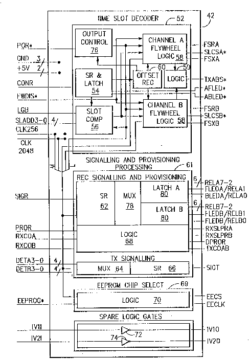
Referring to Figure 7, there is shown a schematic
diagram of the time slot decoder 52. The output
control 76 shown in Figure 4, receives the POR* signal
and includes NAND gates 84, 86 and 88 which receive
POR* which forces a high level at outputs SLCSA*,
SLCSB* and TXABS* respectively when the POR* signal is
low. The POR* signal is also provided to an inverter
90 having an output connected to NOR gates 92, 94, 96
and 98 for forcing low-level outputs on FSRA, FSXA,
FSRB and FSXB when the POR* signal is low. The POR*
signal is provided to a flip-flop 100 having an output
connected to inverter 102, which is further connected
to inverter 104. Inverter 104 provides an output LPOR*
which is connected to the EEPROM chip select 69, as
shown in Figure 6 and is further connected to a clear
input of a latch circuit 106 which drives the AFLED*
and ABLED* signals. The clear input holds the latch
outputs low when the POR* signal is low. The output of
inverter 104 is also connected to preset, PR*, inputs
of shift register 134, latch 60 and flip-flop 154 and
covers their outputs to go high when POR* is low.
-40-
2031793
The shift register and latch 54 functions as a
serial-to-parallel converter. Circuit 108 receives the
CONR data which is clocked in at 2.048 Mb/s to eight D-
flops forming the shift register. The outputs of the
eight D-flops are fed to the first inputs of the eight
2-input D-flops which form the latch. The input
selects of the 2-input D-flops are enabled by a bit 0
strobe from a delay circuit 110 so that at bit o of
each time slot the CONR data from the previous time
slot enters the DIl input. After bit 0, the input
selects change and input DI0 is active and receives a
fed-back output forming a latch. Delay circuit 110 is
formed of seven D-flops and is used to delay the 256
KHz clock and provide seven outputs representing
strobes occurring at each of bit times 0-6 within each
time slot.
The outputs of the serial-to-parallel converter
108 are distributed throughout the circuit with the
five least significant bits being provided to a
comparator circuit 112, which is part of the slot
comparator 56. The SLADD3-0 inputs and the LGB input
are provided to the comparator circuit 112, where the
five bits are compared. A match is indicated at an
output of comparator 112. A timing strobe output of
comparator 112 is provided to NAND gates 114 and 116
-41-
for the channel A and channel B strobes respectl0ve~y7.9 3
The bit 5 output from the serial-to-parallel converter
108 is provided directly to an input of NAND gate 116
and to an input of an inverter 118, the output of which
is provided to an input of NAND gate 114, thereby
providing information to the NAND gates as to whether
or not the strobe is a channel A or channel B strobe
for an identified line unit. Bit 7 from the serial-to-
parallel converter 108 is provided to an inverter 120,
the output of which is provided to each of the NAND
gates 114 and 116 to indicate to the NAND gates whether
the configuration word CONR is providing time slot
information or offset information. The outputs of the
NAND gates 114 and 116 are provided to inverters 122
and 124 respectively, which inverters have outputs
connected to the channel strobe CHSTR input for each
flywheel circuit 58 for channels A and B of the line
unit.
The five least significant bit outputs from the
serial-to-parallel converter circuit 108 are also
provided to an offset register 60 and a five-bit
comparator circuit 126, which receives as a second
input a five-bit output from the offset register 60.
Offset register 60 is essentially a five-bit latch
comprising five 2-input D-flops. Bit 7 from the serial-
-42-
2031793
to-parallel converter 108, which when high indicates
offset information is being transmitted, is connected
to a NAND gate 128, as is the bit 1 output strobe from
delay circuit 110. The output of NAND gate 128 is
connected to an inverter 130 and an input of a flip-
flop 132. The output of inverter 130 is connected to
an enable input of a two-bit shift register 134 and to
an input of a NAND gate 136.
Shift register 134 receives an input through an
inverter 138 from the output of comparator circuit 126,
which indicates whether or not the offset number has
changed from the number in register 60. Shift register
134 also receives a preset input from inverter 104
which can essentially disable the register. The bit 7
output from the serial-to-parallel converter 108 is
also provided to an input of a NAND gate 140, which
also receives the bit 2 strobe from the delay circuit
110. NAND gate 140 provides an output during bit time
2 to inverter 142 when offset information is being
received. The output of inverter 142 is provided to a
NAND gate 144 along with the outputs of the shift
register 134. Shift register 134 is a two-bit shift
register and will provide two zero outputs when two
identical offset numbers have been detected from
comparator 126. The output of NAND gate 144 is
-43-
2031 793
provided to an enable input of shift register 60
through an inverter 146 to enable the register, so that
a valid offset number may be latched therein and
provided at an output to an offset input of both
flywheel circuits 58. Register 60 also receives as a
preset input the output of inverter 104 to disable the
register. The output of NAND gate 144 is connected to
a clear input of flip-flop 132 providing an indication
thereto that a new offset number was latched into
register 60. An output from flip-flop 132 is provided
to the BKTXS inputs of the flywheel circuits 58. The
purpose of this output is to disable transmit strobes
immediately after a new offset number is latched.
The two outputs of shift register 134 are provided
to the inputs of a NOR gate 148, the output of which is
provided to an inverter 150 and an input of NAND gate
136. The inputs to NAND gate 136 provide logic
indicating whether the input CONR byte contains offset
information or time slot information, and whether two
identical bytes have been received. The output of NAND
gate 136 is provided to an inverter 152, the output of
which is provided to the enable input of latch 106.
Latch 106 receives bits 5 and 6 from the output of the
serial-to-parallel converter 108, which bits are
indicative of the auxiliary card being busy or failed,
- 20317g3
and provides two output bits to the AFLED* and the
ABLED* outputs.
A flip-flop 154 receives as a preset input the
output of inverter 104. The output of inverter 150 is
provided to a clear input, which clears the flip-flop
after two matched offset numbers have been received,
which should occur two frames after circuit
initialization. The output from flip-flop 154 is
connected to OPCONT inputs of flywheels 58. The OPCONT
signal provides for power up disable of the flywheel
and also disable until valid offset number are latched.
Bit 6 from the serial-to-parallel converter 108,
which represents the EEPROM chip select bit, is
provided to an input of a two-input flip-flop 156. A
NAND gate 158 receives a bit 5 strobe from the delay
circuit 110 and bit 7 from the serial-to-parallel
converter 108, which indicates whether the byte
contains time slot information or offset information.
Select inputs on flip-flop 156 are connected
respectively to the inputs and outputs of an inverter
160, which receives the output of a NAND gate 162.
Inputs to NAND gate 162 are derived from a bit 1 strobe
out of delay circuit 110 and the channel A strobe from
inverter 122. The output of flip-flop 156 is provided
to an input of a NOR gate 164, which has an output
-45-
2031793
connected to an inverter 166 which provides the EECSB
signal which is directed to the EEPROM chip select 69.
A flip-flop 168 identical to flip-flop 156 is connected
in an identical manner as flip-flop 156, with the
exception that NAND gate 172 has an input connected to
the channel B strobe instead of the channel A strobe.
The output of flip-flop 168 is connected to an input of
NOR gate 164.
The flywheel circuits 58 receive a number of
additional strobes and clock signals as, for example,
bits 1, 2 and 5 from the delay circuit 110, the 256 KHz
clock and two clock inputs, both of which receive the
2.048 MHz clock. The flywheel disable FWDIS* signal is
provided to the flywheel circuit also. The flywheel
circuit 58 for channel A provides an RXSlB output to
NOR gate 92, which provides the FSRA output. An output
RXS8B from the flywheel circuit for channel A provides
the CAR8B output. The channel A flywheel circuit
provides an SLCS output to NAND gate 84, which provides
the SLCSA* output. A TXSlB output from the channel A
flywheel circuit is provided to NOR gate 94, which
generates the FXSA output. A TXS8B output from the
channel A flywheel circuit provides the CAT8B output.
A TXTS output is provided to an input of a NOR gate
174.
-46-
203179~
Outputs from the flywheel circuit for channel B
are similarly connected to provide the outputs FSRB,
SLCSB*, FSXB, CBR8B and CBT8B. An output of NOR gate
174 is connected to a two-input D-flop 176 which has
its select inputs connected to the input and output of
an inverter 178, the input of which is fed by the 256
KHz clock. The output of flip-flop 176 is connected to
an input of a flip-flop 180 which has an output
connected to an input of NAND gate 88 which generates
the TXABS* output.
Referring to Figure 8, there is shown a schematic
diagram for a flywheel circuit 58. The circuit is
centered around a five-bit counter 182 which receives a
2.048 MHz clock signal but is only enabled during bit
time 2, when it receives a bit time 2 strobe from input
BITTIM2. While in a steady state with the clock
synchronized with a previous channel strobe, the clock
repeatedly counts from 0 to 31 and provides outputs to
a 0 and 31 detector 184, which provides at output DZH a
high-level activation strobewhen the input count is 0
and provides at an output D3lL a low output when the
input count is 31. The DZH output is connected to a
NAND gate 186, which also receives an input from the
256 KHz clock to provide an output to a flip-flop 188
which generates the receive strobe, RXSlB. The flip-
-47-
2031793
flop 188 also has a preset input PR connected to the
output of an inverter 190, which is connected to the
output of a NOR gate 192, which receives as one input
the output control signal OPCONT. Thus, the five-bit
counter 182 causes receive strobe signals to be
continuously generated under the assumption that it is
properly synchronized with an input channel strobe
CHSTR. The OPCONT signal can disable flip-flop 188 on
power up, or if there are more than two channel strobes
per frame, or if there are no channel strobes per
frame.
The counter may be re-synchronized to a channel
strobe, CHSTR, arriving during a new time slot after
the strobe appears in the new time slot for two
frames. This is accomplished through the use of a two-
bit shift register 194. The two-bit shift register has
its input connected to output D31L of detector 184 and
receives a O signal during count 31 of the five-bit
counter. The enable input of shift register 194 is
connected to the output of an inverter 196 which is
further connected to the output of a NAND gate 198.
NAND gate 198 receives as one input the channel strobe,
CHSTR, and as a second input a bit 1 strobe BITTIMl.
Thus, during bit 1 of a time slot having a channel
strobe, the shift register 194 is enabled and will
-48-
2031793
normally enter the 0 level at output D3lL of detector
184, thereby providing a 0 at output OP0 of the shift
register. If the channel strobe CHSTR appears in a
time slot other than the one to which the counter is
synchronized, the output from the detector 184 will not
be low when register 194 is enabled, and the register
will be incremented to provide a 1 output at OP0. If a
second channel strobe arrives out of sync with the five-
bit counter, the shift register 184 will again be
incremented to provide two l-level outputs.
It should be noted that the detection of the 0-
level output of detector 184 occurs at a count of 31,
which is essentially one time slot prior to the time
when the channel strobe should occur. This is
permissible because the counter 182 is not enabled and
does not increment until the bit 2 time provided by
BITTIM2. Thus, the counter is incremented one bit time
after the output of the detector 184 is sensed.
A NAND gate 200 receives four inputs, including
the two outputs of the 2-bit shift register 194, the
channel strobe, CHSTR, and the bit time 2 strobe
BITTIM2. The output of NAND gate 200 is connected to a
clear input of the five-bit counter 182. Thus, if two
channel strobes are found not to be in sync with the
five-bit counter, the counter is then cleared during
-49-
2031793
bit time 2, when the next channel strobe occurs,
thereby re-synchronizing the five-bit counter to the
new channel strobe.
Shift register 194 has a preset input connected to
the FWDIS* flywheel disable signal, which is low when
the flywheel is to be disabled. A low input on the
preset causes both outputs of 194 to go high, with the
result that the counter 182 is cleared each time a
channel strobe, CHSTR, arrives at NAND gate 200.
Clearing the counter provides a zero output or count
which, as mentioned earlier, provides a receive strobe
output RXSlB. Thus, the flywheel is disabled and a
receive strobe is generated for each input CHSTR.
As mentioned earlier, the five-bit counter 182
will continuously generate strobe outputs but can be re-
synchronized to a new channel strobe time slot by the
occurrence of a new channel strobe for two frames.
Provisions must be made to disable the receive strobes
if the channel strobe, CHSTR, ceases for two frames.
To provide this capability, two 2-input D-type flip-
flops 202 and 204 are provided. Flip-flop 202 receives
at an input DI1 the channel strobe, CHSTR, through an
inverter 206. Select inputs SI and SI* are provided
with inputs sensitive to the DZH signal from detector
184 and a bit time 5 signal. A NAND gate 208 receives
-50-
2031793
the DZH signal and the bit time 5 strobe, BITTIM5, so
that the DZH signal is sensed after the counter 182 has
been incremented at bit time 2. An output of NAND gate
208 is provided to the SI* input of flip-flop 202 and
to an inverter 210, the output of which is provided to
the SI input of flip-flop 202, so that during bit time
5, when the counter is at 0, the channel strobe, CHSTR,
will be entered into the flip-flop as a 0-level
signal. When bit time 5 ends, the input of the flip-
flop 202 switches to DI0, which receives its input from
the output of the flip-flop, thus maintaining the
output of flip-flop 202 at a 0 level. If the channel
strobe was not present, a 1-level signal would enter
flip-flop 202 at input DI1, generating a 1-level output
which would be maintained after the signals to the
select inputs shift at the termination of the bit 5
strobe or when the DZH goes low. The output of flip-
flop 202, while being fed back to input DI0, is also
fed to an input of multiplexer 212, which input would
normally be fed to the output and to an inverter 214,
the output of which is connected to the DI1 and clear
input of flip-flop 204. If the output of flip-flop 202
is 0, this will appear as 0 at the DIl and clear inputs
of flip-flop 204, resulting in a 0-level signal at its
output. The input select signals of flip-flop 204 are
-51-
203179~
connected to the input select signals of flip-flop 202;
therefore the inputs will switch simultaneously with
flip-flop 202, and the 0-level signal at the output
will be maintained and fed back to the input DI0.
If a channel strobe was missing and flip-flop 202
was set to the 1 state, this would appear at the DIl
input of flip-flop 204 and be ready to be clocked in at
the next frame, when the input is switched from DI0 to
DI1. If, in the next frame, the channel strobe is
still missing, the output of flip-flop 202 will remain
1, and the output of flip-flop 204 will change to a 1
level. If perchance the channel strobe had returned to
its proper timing, flip-flop 202 would revert back to a
0-level output, while flip-flop 204 would clock in the
1-level signal during bit time 5 but would immediately
thereafter receive the 0-level output from flip-flop
202 at its clear input, so that by bit time 7 the
output of flip-flop 204 would be cleared to a 0 level.
The output of flip-flop 204 is connected to an
input of NOR gate 192, so that when the output is at a
1 level, the flywheel outputs are disabled`, as
previously mentioned in regard to the function of
signal OPCONT. Thus, flip-flops 202 and 204 function
to disable the outputs if the channel strobe, CHSTR, is
missing for two consecutive frames.
-52-
2031793
The select input of multiplexer 212 is connected
to the flywheel disable FWDIS* signal so that when the
flywheel disable signal is low, the multiplexer 212
receives its input from the output of inverter 206 to
essentially by-pass flip-flop 202. Flip-flop 204 will
continue to function and provide an output level 1, if
the channel strobe CHSTR does not occur when DZH is
high, to thereby disable the outputs.
A NAND gate 216 is connected to receive the two
outputs of the shift register 194 and the flywheel
disable signal, so as to provide a 0-level output only
when the flywheel is not being disabled and when the
counter is being re-synchronized by the occurrence of
two l-level signals from the shift register 194. The
output of NAND gate 216 is connected to the preset
inputs of both flip-flops 202 and 204 to effectively
drive the outputs to a 1 level and thereby disable the
strobe outputs from the circuit. This disable signal
will continue until the counter is re-synchronized with
the incoming channel strobe and at least one of the
outputs of shift register 94 reverts to a 0 level.
Thus, no strobe outputs are provided during a re-
synchronization time.
-53-
- 2031793
During normal operation, the receive strobe lS
essentially initiated by a high on the DZH output
detector 184. This output is provided to an input of a
variable shift register 218 which functions to delay
the receive strobe by a number of time slots
corresponding to the offset number received at the
offset input. A circuit diagram for a variable shift
register is shown in Figure 9 and will be described
subsequently. The variable shift register receives the
256 KHz clock and the 2.048 MHz clock and provides an
output to a NAND gate 220, which also receives inputs
from the 256 KHz clock and an input BKTXS signal. NAND
gate 220 provides an output to a flip-flop 222, which
generates the transmit strobe TXSlB. Flip-flop 222
also receives the 2.048 MHz clock and the output of
inverter 190 is provided to a preset input which
functions to disable the flip-flop.
The BKTXS input to NAND gate 220 is generated by
flip-flop 132 of Figure 7, which functions to disable
the transmit strobes for one frame after a new offset
number is received to prevent erroneous transmit
strobes from being generated.
The output of NAND gate 220 is connected to a NOR
gate 224 which has a second input connected to the
output of inverter 190 and provides the output TXTS
-54-
203179~
-
indicating the occurrence of a transmit time slot. The
output of NOR gate 224 is essentially disabled by a
high output from inverter 190.
Flip-flop 226 has its input select inputs
connected to the 256 KHz clock so that SI receives the
clock directly and SI* receives it through an inverter
228. Input DIl receives the output of NAND gate 186
corresponding to a receive strobe output. The output
of flip-flop 226 is fed back to the input to maintain
the same state, and the inverted output is connected to
a flip-flop 230 which provides the SLCS SLIM chip
select signal.
A flip-flop 232 has its DIl input connected to the
output of NAND gate 186 and its DI0 input connected to
its output. A preset input is connected to an output
of an inverter 234 which has its input connected to
inverter 190 for disabling the flip-flop as previously
discussed. The input select inputs of flip-flop 232
are connected to the same input select signals as flip-
flop 226 so as to activate input DIl to receive the
output of NAND gate 186 during the generation of a
receive strobe. The inverted output of flip-flop 232
is connected to an inverter 236 which is connected to
another inverter 238 to provide the RXS8B output
signal.
2031733
A flip-flop 240 is connected in a manner similar
to flip-flop 232, with the exception that the DI1 input
is connected to the output of NAND gate 220 to receive
a transmit strobe signal. The inverted output of flip-
flop 240 is connected to inverters 242 and 244 to
provide the TXS8B output signal.
Referring to Figure 9, there is shown a schematic
diagram of the variable shift register 218. The
variable shift register is used to delay the receive
strobe by a variable number of time slots to generate
the transmit strobe. The receive strobe signal is
provided to the DI input from the DZH output of
detector 184. The receive strobe can be delayed from 0
to 31 time slots in accordance with an offset number
provided by the offset register 60 in Figure 7. The
offset number is a five-bit number provided at the
offset input. The variable shift register receives the
2.048 MHz clock and the 256 KHz clock. The shift
register comprises a plurality of flip-flops 246 which
are essentially arranged to form a one-bit shift
register 248, a two-bit shift register 250, a four-bit
shift register 252, an eight-bit shift register 254 and
a 16-bit shift register 256. The five offset bit lines
are connected to five 2-input multiplexers 258-266,
representing the least to the most significant bits of
-56-
- 2031793
the offset number. Multiplexer 266 has a first input
connected directly to the DI input to receive the
receive strobe. A second input of multiplexer 266 is
connected to the output of the 16-bit shift register.
The output of the multiplexer provides the DI input
without delay if the select input, the most significant
bit of the offset number, is 0. The multiplexer
provides the DI input delayed by 16 time slots if the
select input receives a l-level signal from the most
significant bit of the offset number. The output of
multiplexer 266 is connected to an inverter 268, the
output of which is connected to an input of multiplexer
264, the other input of which is connected to the
output of the eight-bit shift register 254. The input
of the eight-bit shift register 254 is also connected
to the output of the inverter 268. Depending upon the
setting of the multiplexer 264, the DI input is delayed
another eight time slots, or bypasses the eight-bit
shift register. In like manner, the output of
multiplexer 264 is connected to an inverter 270, the
output of which is connected to the input of the four-
bit shift register 252 and to an input of the
multiplexer 262, the other input of which is connected
to the output of the four-bit shift register 252.
Multiplexer 262 functions to either bypass the four-bit
20~1793
shift register or to pass the DI input through the
shift register to provide an four additional time slots
of delay. Multiplexers 262, 260 and 258 each have
outputs connected to inverters 272-276 respectively,
and multiplexers 260 and 258 function in a manner
similar to the other multiplexers to either bypass
their associated shift registers or pass the DI input
through the shift register to provide additional delay.
Thus, the variable shift register can be set to
provide any delay time from 0-31 time slots, depending
upon the five-bit offset number received at the offset
input.
Thus, the line unit interface circuit of the
present invention performs all of the functions
necessary to interface a line unit to the TSA via the
line unit interface bus. These functions include the
generation of a plurality of framing and timing signals
necessary to process signaling, provisioning and
configuration data provided by the TSA. A major
function of the LUC is to decode the configuration data
for the purpose of time slot assignment and for
establishing an offset number pertaining to the time
delay between a receive strobe and a transmit strobe.
-58-
20317~3
A variable shift register is utilized to provide a
delay between the receive and transmit strobes which
corresponds to the offset generated by the TSA. A
flywheel circuit is provided for preventing the
erroneous assignment of time slots resulting from noise
or false signals received on the line unit interface
bus from the TSA.