Note : Les descriptions sont présentées dans la langue officielle dans laquelle elles ont été soumises.
cA2n3 1 966
APR 1 8~
- 1 -
IMPROVED INTERFERENCE SUPPRESSION IN OPTICAL
COMMUNICATION SYSTEMS
This invention relates to optical tr~n~mi~ion systems, and more
particularly, to a technique for suppressing mutually induced interference between
S closely spaced electrical signals on a Photonic Integrated Circuit (PIC).
Conventional optical communications systems will be described
hereinbelow in conjunction with the drawings.
The foregoing problem in the prior art has been solved in accordance
with the present invention which relates to a technique for suppressing mutually10 in~ ce~l interference between closely located electrical tr~n~mi~ion paths on, for
example, a PIC.
In accordance with one aspect of the invention there is provided a
network interface unit (NIU) for interfacing an electrical device to an optical
network, said NIU comprising: first and second electrical tr~n~mis~ion lines,
15 arranged to effectuate substantial electromagnetic coupling therebetween; electro-
optical converting means connected to said first electrical tr~n~mi~ion line forreceiving a first electrical signal and converting the first electrical signal into a first
optical signal for tr~n~mi~sion to the optical network; optical-electro converting
means for (a) receiving a second optical signal from the optical network, (b)
20 converting said second optical signal into a second electrical signal, and (c)
transmiKing said second electrical signal via the second electrical tr~n~mi~cion line;
and means connected to said second electrical tr~n~mi.~sion line for increasing a
ratio of energy in the second electrical signal to energy electromagnetically coupled
from said first electrical tr~n~mi~ion line to said second electrical tr~n~mi~ion
25 line.
In accordance with another aspect of the invention there is provided a
method of providing immunity against interference in two spatially separate
channels comprising the steps of: (a) converting all energy in a signal to be
transmitted on a first one of the spatially separate channels into a first
`CA203 1 966
APR 1 81~9~
- la-
predetermined state, for generating a converted electrical signal, (b) transmitting the
converted electrical signal along the first spatially separate channel, (c) increasing,
in the second of the spatially separate channels, a ratio of energy in a second
predetermined state which is prop~g~ting along the second of the two spatially
5 separate channels to interference caused by energy in the first predetermined state.
-2-
It is a particular aspect of one ~ bo iilll~llL of the invention to
eliminate the interference between the electrical signal input to an E/O converter
and the electrical signal output from an O/E converter which propagate adjacent
to each other on a PIC. In accordance with the invention, the electrical signal
5 used to drive the E/O converter is first electrically modulated before entering the
PIC to produce a new electrical signal in a different frequency band from the
original electrical signal. The new electrical signal is then supplied to the PIC and
used to drive the E/O converter. This technique guarantees that the signal exiting
from the O/E converter and the signal entering the E/O converter are in separate10 frequency bands, at least while they are both on the PIC. Any crosstalk can then
be eliminated with electrical filtering techniques which can be imrl~m(-nt~
external to the PIC. In other ~ , the electrical modulator is replaced
with an encoder, and the illLt;lL~ is suppressed using a selective decoder,
rather than the filtering techniques referred to above.
15 Brief Description of the DrawinYs
FIG. 1 shows a typical optical ~ l "",;. ,~linns system of the prior
art;
FIG. 2 shows an optical -".,.,. ,;.,.1;ll.,~ system utilizing an
improved Network Interface Unit (NIU) in a~,ulddll~, with the present invention; and
FIG. 3 shows an NIU which may be connected to the NIU of
FIG. 2.
Optical ~Idll~ ;vl. media have emerged as the preferred
~lall~ ;Oll media. Relatively large bandwidth, low cost and ease of
;- ,~ are just a few of the reasons which have cnntrihl-t(-d to making
optical media so preferable.
Use of optical Lldll~ ,iol~ media usually requires utilization of
electro-optical (~/O) converters to convert an electrical input signal into an optical
signal for lldll~ ;(JII over an optical medium. For full duplex - ",..."".:. ~I ;nn~
30 the optical medium may comprise a separate fiber for each direction, or
alternativeiy, may utilize a single fiber and some " l~ ;"~ scheme. One such
system is described in "Two Fibers or One? (A Comparison of Two-Fiber and One-
Fiber Star Al~ ulc~ for Fiber-to-the Home A,, ' )" by Loria Baskerville
-3--
in Jou}nal of Li htwave Technolo~v. Vol.7, No. 11, Nov. 1989, and is shown in
block diagram form in FIG. 1. The system of FIG. 1 comprises (a) Electro-Optical(E/O) eonverters 101-102, (b) Optical-Eleetro (O/E) eonverters 103-104, (e) optieal
L~ ;ull medium 105, (d) direetional couplers 106-107, and (e) shielding 108-
5 109, which is not shown in the above reference but is normally utilized in suchsystems. E/O converter 101 and O/E converter 104 are normally imrl~-nn~-nf~-d on
a signal eireuit eard, as shown in FIG. 1. Similarly, E/O eonverter 102 and O/E
eonverter 103 are also normally i .l,l.. llr-i on a single eireuit eard. The system
of FIG. 1 is intended to provide full duplex - ,.... " ~ between end users.
In operation, an eleetrieal input signal arrives at E/O eonverter 101
and is used to drive a laser having an optieal output frequency band centered atF1. The optical output signal is then transmitted over optical medium 105 and
received at O/E converter 103, which converts it back to an electrical signal and
forwards the electrical signal to an end user equipment. Similarly, E/O converter
15 102 receives an electrical input signal which it converts to an optical output signal
having a frequeney band centered at F2. The optical output signal is then
Lldll~ cd over optical medium 105 from E/O converter 102 to O/E converter
104, where it is converted back to an electrical signal.
Eaeh reeeiver must eontend with interferenee from two different
20 sourees. First, as FIG. 1 shows, light whieh is ~ld.-~ d from E/O eonverter 101
enters optieal medium 105 by means of directional coupler 107. However, a
portion of this light is reflected back toward O/E converter 104 due to imperfect
splicing in the fiber, Rayleigh scattering, imperfections in the directional coulers, or
other i~ clrc~iull~ in the system. These reflections cause i~clrclcl-~C in O/E
25 eonverter 104. This problem has been solved in the prior art by, for example,employing an optieal filter between direetional eoupler 107 and O/E eonverter 104
whieh suppresses F1 and passes F2. Alternatively, a wavelength selective
direetional eoupler could be employed. Seeond, eleetrieal signals entering E/O
eonverter 101 interfere, due to ul-dc~ blc .,lc~,Ll.,lll..5.-ctie eoupling, with eleetrical
30 signals exiting O/E converter 104, and cause il.Lc-rc-c--~c. This second problem
..,
- 3 a -
- has been solved in the prior art through the use of shielding 108, which serves to
attenuate crosstalk between electrical signals exiting O/E converter 104 and
electrical signals entering E/O converter 101. E/O converter 102 and O/E
converter 103 interfere in a similar manner, with a similar solution as shown in5 FIG. 1.
The use of shielding 108 and 109 is d;~alvdllL.A~,_vu~ for several
reasons. First, it has recently become possible to fabricate both an E/O converter
and an O/E converter on a single chip, known as a Photoconic Integrated Circuit
(PIC). PICs provide significant cost and space savings. Further, alignment of
10 optical waveguides on a PIC can be done l ' ':-ho~raphically, rather than
manually, thereby making exact alignment easier. Because of space constraints onthe PIC, however, it is extremely difficult to implement proper shielding. Further,
the shielding used in current systems does not provide the desired amount of
~llr~ ". and thus, there always remains some crosstalk and il.~c-rclGllce. The
15 shielding problem is extremely severe on a PIC because the O/E converter and the
E/O converter are so closely located, and space is not available to apply the
shielding. Thus, standard techniques for eliminating crosstalk between the
electrical signals work only in the prior art technology, e.g., on a circuit card, and
are of little value in state of the art PIC technology. This problem has greatly20 hindered the development of PICs.
The problem that remains in the prior art is to provide a method of
reducing the ill~,.rclc.lc., between the electrical signals entering the E/O converter
and the electrical signals exiting the O/E converter, where extreme space
limitations exist, such as on a PIC.
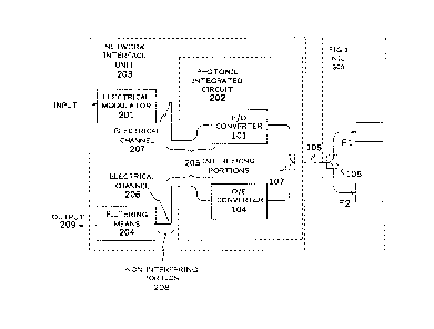
FIG. 2 shows a block diagram of an exemplary optical
,.,.... ,.,.,.;. ~lion system, utilizing a Network Interface Unit (NIU) 203 in accordance
with the present invention. The NIU 203 includes (a) Electro-Optical (E/O)
converter 101, (b) O/E converter 104, (c) filtering means 204, and (d) electrical
modulator 201. Other labelled portions of FIG. 2 will be explained hereafter. The
system of FIG. 2 is shown without shielding, however, shielding may be
i...l,l~ ..-f ..lrd in ~ , with the present technique to further improve
~,f'.r..- ~--c
-3b-
- In operation, an input electrical signal is received at electrical
modulator 201 which modulates the input electrical signal to a first predetermined
frequency band to create a new electrical output signal. The new electrical output
signal is then sent to E/O converter 101, via electrical channel 207, where it is
S converted ~o--
optical signal centered at the exemplary frequency band Fl, for r over
optical waveguide 105.
Optical signals to be received by NIU 203, which are transmitted from
other NlUs in the system, are first received in frequency band F2 from optical
5 ~ medium 105 and directional coupler 107 by O/E converter 104 and are
converted into electrical output signals. The electrical output signal s are then
transmitted over electrical channel 206 to filtering means 204. T r in
channel 206 is caused by the electrical signal in channel 207 in two ways. First,
while traveling along portion 205 of electrical channel 206, the electrical signal in
10 channel 206 picks up r from the other electrical signal, previously
discussed, which is traveling on portion 205 of electrical channel 207. Second, light
emitted from E/O converter 101 at frequency band F1, which is an optical version of
the electrical signal on channel 207, is partially reflected back to O/E converter 104.
However, once the O/E converted signal traveling on electrical channel 206 reaches
15 portion 208 of electrical channel 206, ' "y no more r ~ C is picked up
from the signal on electrical channel 207 from either of the two previously
mentioned sources. Portions 208 of electrical channels 207 and 206 may be
prevented from interfering with each other by shielding or by spacing them far
enough apatt. Portion 208 is disposed off the PIC as shown, so severe space
20 limitation is not a problem. It should also be noted that interfering portion 205 may
extend off the PIC.
Filtering means 204 is tuned to suppress substantially all energy in the
first 1~ frequency band and, ideally, should be disposed anywhere along
the n~,.. r ' V portion 208 of electrical channel 206. Therefore, filtering means
25 204 outputs an electrical signal on output 209 which is ~ ' 'ly free from
r caused by the signal on electrical path 207.
Note dhe dashed oudine in FIG. 2 labeled Photonic Integrated Circuit
(PIC) 202. When the E/O converter and the O/E converter are on the same PIC, themedhod is p~i ' 'y a~ due to dhe fact dhat prior art shielding methods,
30 previously discussed, are prohibited by a severe limitation in available space. By
utilizing the inventive technique, r ~ caused on PIC 202 is eliminated
external to PIC 202, where more space is available to implement the necessary
hardware.
FIG. 3 shows an NIU 300 comprising similar , as those
35 already discussed in FIG. 2. The NIU of FIG. 3 is suitable for use with dhe NIU of
FIG. 2. More I ' '~" optical signals transmitted by E/O converter 101 of FIG.
2 are received by O/E converter 103 of FIG. 3 and are converted to an electricalsignal, which is output by O/E converter 103 onto electrical channel 303. T.'e
frequency band of this output electrical signal will be detennined by electlicalmodulator 201 of FIG. 2. Filtering means 301 then suppresses energy picked up
5 from the electrical signal being used to drive E/O converter 102. Finally, electrical
~' ~I ' 302 ' ' ' the signal, thereby providing an output signal
"~, free from r Gl.~,G.
E/O converter 102 is used to convert an electrical signal to an optical
signal for, to O/E converter 104 of FIG. 2. O/E converter 104 of FIG. 2
10 then converts the received optical signal to an electrical signal for i over
electrical channel 206 as previously described.
It is to be understood that the example described herein is for illustrative
purposes only and that other variations of the invention can be easily constructed
without violating tbe spirit or scope thereof. For example, electrical modulator 201
15 could be replaced with an encoder, such as a spread spectrum encoder. The spread
spectrum encoder would distribute the energy in the electrical input signal over a
large bandwidth, thereby reducing the amount of energy present in the original
bandwidth. In this case, filtering means 204 would be required to suppress all
energy which was outside the original bandwidth, and thus, would suppress most of
20 the energy from the interfering signal. Filtering means 204 may also include a
spread spectrum decoder for decoding a spread spectrum signal being received by
NIU 203. Analogous changes to other NIUs in the system, such as NIU 300 of FIG.
3, also would be made. In general, any technique that ~ 5 the energy in the
two electrical signals and ' I '~, suppresses a larger fraction of the energy in25 tbe interfering signal than in the desired signal will suffice. It is also possible to
include two ' , one for each direction, and to convert the electrical signals
into t~vo different states rather than converting one of the electrical signals and
leaving the second alone as was described previously herein. Filtering means 204 is
understood to be any device capable of reducing the ratio of interfering energy to
30 desired energy. Again, analogous changes to other NIUs in the system would have
to be made. Both F1 and F2 could even be made equal to each other, as is the case in
some systems. The electrical modulator of FIG. 2 could even be eliminated if theincoming electrical signal to the NIU was already in a state that was ~' " ' ~''from the electrical signal output from O/E converter 104.