Note : Les descriptions sont présentées dans la langue officielle dans laquelle elles ont été soumises.
2~ 031.
LINEAR AMPLIFIER
BACKGROUND OF THE INVENTION
Field of the Invention:
The present invention relates t~ a linear
amplifier, and particularly to a linear amplifier
having good distortion and efficiency characteristics
over semi-microwave and microwave bands which are
employed in satellite communication systems, ground
microwave communication systems and the like.
Description of the Prior Art:
FIG. 1 is a block diagram showing a conventional
linear amplifier disclosed in, for example, "6 GHZ
Adaptive-Type Linearizer for Satellite Communication
Earth Station HPA" by Sato and Kimura on pp. 10-195, at
the national meeting of Institute of Electronics and
Communication, 1986. Referring to FIG. 1, there are
shown an input terminal 1, an output terminal 2, a
high-powered amplifier (HPA) 5, a level control unit
17, a linearizer 18, a linearizer control unit 19 and a
spectrum analyzer 20.
A description will now be made of the operation of
the linear amplifier.
A signal inputted from the input terminal 1 is
applied to the high-powered amplifier 5 via the level
control unit 17 and the linearizer 18 and is outputted
at output terminal 2. Portions of the input signal at
terminal 1 and the output signal of high powered
.~
Z0;~3031.
amplifier 5 are extracted by level control unit 17 and
are applied to linearizer control unit l9.
The linearizer control unit 19 controls the
linearizer 18 to make the levels of the input signal at
terminal 1 and the output of HPA 5 equal to each other
to perform its switching action, and supplies the input
and output signals to the spectrum analyzer 20 which
analyzes the frequency content of these signals.
The linearizer control unit 19 stores therein
information about the frequency spectrum distribution
of the components of the input/output signals measured
by the spectrum analyzer 20 and performs arithmetic
processing on the same, and thereafter supplies data
for controlling the linearizer's characteristics to the
linearizer 18 so that distortion components of the
input/output signals are reduced.
The level control unit 17 includes a variable
attenuator and a variable gain amplifier to correct the
variation in level of each of the signals according to
the control of the linearizer's characteristics so as
to maintain a constant gain for the entire system
comprising the level control unit 17, linearizer 18,
and HPA 5.
The above conventional linear amplifier has a
function for determining the difference between the
frequency spectrum distribution of the input signal and
that of the output signal of the high-powered amplifier
5 to automatically control the linearizer's
characteristics such that the components of unnecessary
distortion are reduced.
Since the conventional linear amplifier is
constructed as described above, it is accompanied by
the problem in that the spectrum analyzer, the
linearizer control unit and the like are necessary
components, so that the overall arrangement is
203;~031.
constructed of large size, the operation efficiency is
low because the high-powered amplifier is operated in a
good linear region well below a saturation region and
the operation rate is slow because data processing is
effected by using digital circuitry applied to the
control of the linearizer, thus leading to difficulty
in the application of the linear amplifier to high-
frequency band communication channels.
SUMMARY OF THE INVENTION
With the foregoing problem in view, it is an
object of the present invention to provide a linear
amplifier constructed in small size and operable at
higher efficiency and at a high-frequency band.
In order to achieve the above object, the linear
amplifier according to the present invention is
constructed such that a first directional coupler, a
variable attenuator, a phase shifter and a high-powered
amplifier connected to an input terminal and a second
directional coupler connected to an output terminal are
arranged in cascade connection, and the comparison in
amplitude and in phase between input and output signals
extracted from the first and second directional
couplers respectively is made to detect the amplitude
and phase distortion of the high-powered amplifier
based on the result of the comparison, thus controlling
the amount of attenuation of the variable attenuator
and the amount of phase shift of the phase shifter in a
manner so as to compensate for the detected amplitude
and phase distortion and controlling a DC/DC converter
such that a drain voltage applied to the high-powered
amplifier becomes high when the output signal is large
in level whereas the drain voltage becomes low when the
output signal is low in level.
Z~;~3031.
The above and other objects, features and
advantages of the present invention will become
apparent from the following description and the
appended claims, taken in conjunction with the
accompanying drawings in which preferred embodiment of
the present invention are shown by way of illustrative
example.
~ BRIEF DESCRIPTION OF THE DRAWINGS
FIG. 1 is a block diagram showing a conventional
linear amplifier;
FIG. 2 is a block diagram depicting a linear
amplifier according to a first embodiment of this
invention;
FIG. 3 is a block diagram illustrating a linear
amplifier according to a second embodiment of this
invention;
FIG. 3A is a block diagram illustrating a linear
amplifier according to a third embodiment of this
invention; and
FIG. 4 is a graph of input~output power
characteristics of an amplifier for explaining the
principle of the present invention.
DETAILED DESCRIPTION
OF THE PREFERRED EMBODIMENTS
Preferred embodiments of this invention will
hereinafter be described in detail with reference to
the accompanying drawings.
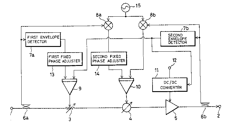
In FIG. 2 illustrating a first embodiment, there
are shown an input terminal 1, an output terminal 2, a
variable attenuator 3, a phase shifter 4, a high-
powered amplifier 5, first and second directional
couplers 6a, 6b, first and second envelope detectors
7a, 7b, first and second phase detectors 8a, 8b, a
2~3~31.
first comparator 9, a second comparator 10, a DC/DC
converter 11, a drain voltage supply terminal 12, a
first fixed phase adjuster 13, a second fixed phase
adjuster 14 and a local oscillator 15.
A description will now be made of the operation of
the first embodiment.
A modulated wave inputted to the input terminal 1
is outputted from the output terminal 2 via the first
directional coupler 6a, the variable attenuator 3, the
phase shifter 4, the high-powered amplifier 5 and the
second directional coupler 6b which are arranged in
cascade connection. Parts of the input and output
signals are extracted by the first and second
directional couplers 6a, 6b, respectively and their
envelope components are detected by the first and
second envelope detectors 7a and 7b respectively.
The envelope component of the input signal is
applied to the first comparator 9 via the first fixed
phase adjuster 13, whereas the component of the
envelope of the output signal is applied directly to
the first comparator 9. The first fixed phase adjuster
13 compensates a fixed phase difference between the
input and output signal caused by their different
transmission paths.
The first comparator 9 compares the envelope
component of the input signal with the envelope
component of the output signal to detect the amount of
amplitude distortion caused by the high-powered
amplifier 5, and based on the result of its comparison,
thereby controlling the variable attenuator 3 in a
manner as to compensate for the amplitude distortion.
The parts of the input and output signals
extracted by the first and second directional couplers
6a, 6b are further applied to the first and second
X~ 31.
phase detectors 8a, 8b, respectively, from which the
phase components of these signals are detected.
The phase component of the input signal is applied
to the second comparator 10 via the second fixed phase
adjuster 14, whereas the phase component of the output
signal is applied directly to the second comparator 10.
The second fixed phase adjuster 14 provides a function
equal to first fixed phase adjuster 13.
The second comparator 10 compares the phase
component of the input signal and the phase component
of the output signal to detect the amount of phase
distortion produced by the high-powered amplifier 5,
and based on the result of its comparison, thereby
controlling the phase shifter 4 in a manner so as to
compensate for the phase distortion.
The DC/DC converter 11 is activated to increase a
drain voltage to be supplied to the high-powered
amplifier 5 based on the envelope component of the
output signal when its amplitude is large, and on the
contrary, to reduce the drain voltage based on the
envelope component of the output signal when its
amplitude is small.
The input/output characteristics for amplifier 5
are shown in the graph of Fig. 4. As shown, higher
drain voltages VD are needed for higher input signal
levels Pia. The efficiency curve for each drain voltage
is also shown. As it is deslred to operate at the
highest or maximum efficiency point of the amplifier
characteristic curve, the Pou;/Pin curve is selected for
various drain voltages according to Ihe input signal
level at the maximum efficiency E)oints. However, these
points correspvnd to the non-linear gain range of the
amplifier. The purpose of the present invention is to
compensate amplitude and phase d stortions of the
amplifier to correct the values of the Pout/Pln curve for
Z~ 031.
each input signal value so as to linearize the Pout/Pin
curve as shown.
FIG. 3 is a block diagram showing a second
embodiment of this invention. In FIG. 3, designated at
numeral 16 is a phase detector. Parts of the input and
output signals are applied to the phase detector 16 via
directional couplers 6a and 6b, where the difference in
phase therebetween is detected. The phase distortion
produced at high-powered amplifier 5 can be compensated
by controlling the phase shifter 4 in accordance with
the phase-difference detection signal produced by the
phase detector 16. The amplitude of the input signal
is compensated similarly as in FIG. 2.
FIG. 3A shows a third embodiment of the invention
wherein a second fixed phase adjuster 14 is provided to
the output of phase detector 16 to compensate a fixed
phase difference caused by the transmission path.
According to this invention, as has been described
above, parts of the input and output signals are
extracted to carry out the comparison in amplitude and
in phase therebetween, thus detecting the amplitude
distortion and the phase distortion based on the result
of the comparison. Then, the variable attenuator and
the phase shifter are controlled so as to compensate
for the amplitude distortion and the phase distortion.
The present invention can therefore bring about
advantageous effects in that the circuit of the linear
amplifier can be simplified in structure and reduced in
size as compared with that of the conventional linear
amplifier, and the linear amplifier is applicable to a
high-speed and high-frequency band operation because of
an all-analog system free from the use of digital
arithmetic processing. Further, the present invention
can also bring about an advantageous effect in that the
operation efficiency can be rendered high because the
2~33a~l.
drain voltage is controlled by the DC/DC converter
while following the level of output power.
Having now fully described the invention, it will
be apparent to those skilled in the art that many
changes and modifications can be made without departing
from the spirit or scope of the invention as set forth
herein.