Sélection de la langue

Search

Sommaire du brevet 2033780 

Énoncé de désistement de responsabilité concernant l'information provenant de tiers

Une partie des informations de ce site Web a été fournie par des sources externes. Le gouvernement du Canada n'assume aucune responsabilité concernant la précision, l'actualité ou la fiabilité des informations fournies par les sources externes. Les utilisateurs qui désirent employer cette information devraient consulter directement la source des informations. Le contenu fourni par les sources externes n'est pas assujetti aux exigences sur les langues officielles, la protection des renseignements personnels et l'accessibilité.

Disponibilité de l'Abrégé et des Revendications

L'apparition de différences dans le texte et l'image des Revendications et de l'Abrégé dépend du moment auquel le document est publié. Les textes des Revendications et de l'Abrégé sont affichés :

  • lorsque la demande peut être examinée par le public;
  • lorsque le brevet est émis (délivrance).
(12) Brevet: (11) CA 2033780
(54) Titre français: STRUCTURE DE TRANSISTOR MINCE A ISOLANT DIELECTRIQUE A FAIBLE RESISTANCE DE COLLECTEUR MONTEE SUR UN ILOT
(54) Titre anglais: THIN, DIELECTRICALLY ISOLATED ISLAND RESIDENT TRANSISTOR STRUCTURE HAVING LOW COLLECTOR RESISTANCE
Statut: Périmé et au-delà du délai pour l’annulation
Données bibliographiques
(51) Classification internationale des brevets (CIB):
  • H01L 29/73 (2006.01)
  • H01L 29/08 (2006.01)
  • H01L 29/732 (2006.01)
  • H01L 29/78 (2006.01)
(72) Inventeurs :
  • BEASOM, JAMES D. (Etats-Unis d'Amérique)
(73) Titulaires :
  • HARRIS CORPORATION
(71) Demandeurs :
  • HARRIS CORPORATION (Etats-Unis d'Amérique)
(74) Agent: AVENTUM IP LAW LLP
(74) Co-agent:
(45) Délivré: 1996-07-30
(22) Date de dépôt: 1991-01-08
(41) Mise à la disponibilité du public: 1991-07-09
Requête d'examen: 1991-05-29
Licence disponible: S.O.
Cédé au domaine public: S.O.
(25) Langue des documents déposés: Anglais

Traité de coopération en matière de brevets (PCT): Non

(30) Données de priorité de la demande:
Numéro de la demande Pays / territoire Date
461,715 (Etats-Unis d'Amérique) 1990-01-08

Abrégés

Abrégé anglais


The occupation area and thickness of dielectrically isolated
island-resident transistor structures, which employ a buried
subcollector for providing low collector resistance at the bottom
of the island, are reduced by tailoring the impurity concentration
of a reduced thickness island region to provide a low resistance
current path from an island location directly beneath the base
region to the collector contact. The support substrate is biased at
a voltage which is less than the collector voltage, so that the
portion of the collector (island) directly beneath the emitter
projection onto the base is depleted of carriers prior to the
electric field at that location reaching BCVEO, so as not to
effectively reduce BVCEO. Since the support substrate bias
potential depletes some of the region of the island beneath the
base region of carriers, the doping of the island can be increased
compared to the case where the substrate is not biased, while
maintaining the electric field at this location less than the BVCEO
field.

Revendications

Note : Les revendications sont présentées dans la langue officielle dans laquelle elles ont été soumises.


WHAT IS CLAIMED
1. A semiconductor device comprising:
a semiconductor substrate having a dielectrically isolated
island region of semiconductor material of a first conductivity
type;
a first semiconductor region of a second conductivity type,
opposite to said first conductivity type, formed in a first surface
portion of said island region, such that semiconductor material of
said first conductivity type of said island region extends beneath
said first semiconductor region and thereby separates a bottom
portion of said first semiconductor region from a bottom portion of
said island region, and wherein the impurity concentration of said
island region is greater at an interface with said first
semiconductor region than at said bottom portion of said island
region;
a second semiconductor region of said first conductivity type,
formed in a first surface portion of said first semiconductor
region; and
wherein said substrate is established at a bias potential,
relative to the potential of said island region, such that a
portion of said island region which extends beneath said first
semiconductor region and separates a bottom portion of said first
semiconductor region from a bottom portion of said island region is
depleted of carriers prior to the occurrence of a breakdown voltage
field between said island region and said first
17

semiconductor region in the presence of a voltage bias differential
applied between said island region and said first semiconductor
region.
2. A semiconductor device according to claim 1, wherein that
portion of said island region having said greater impurity
concentration has a depth deeper than the depth of said first
semiconductor region in said island region, so as to extend beneath
the bottom of said first semiconductor region.
3. A semiconductor device according to claim 1, wherein said
island region has a graded impurity concentration profile
decreasing from the surface of said island region and extending to
a depth deeper than the depth of said first semiconductor region in
said island region, so that the lowest impurity concentration of
said island region occurs beneath the bottom of said first
semiconductor region.
4. A semiconductor device according to claim 3, wherein the
entire thickness of said island region has said graded impurity
concentration profile.
5. A semiconductor device according to claim 2, wherein said
island region includes a third semiconductor region of said first
conductivity type disposed beneath said greater impurity portion of
said island region and having an impurity concentration less than
that of said greater impurity concentration portion.
18

6. A semiconductor device according to claim 1, wherein that
portion of said island region having said greater impurity
concentration has a depth less than the depth of said first
semiconductor region in said island region, so as to intersect a
side portion of said first semiconductor region.
7. A semiconductor device according to claim 1, further
including a channel of material dielectrically isolated from said
substrate and said island region, disposed adjacent to said island
region.
8. A semiconductor device according to claim 7, wherein said
channel of material is biased at a voltage different from that of
said substrate.
9. A semiconductor device comprising:
a semiconductor substrate having a dielectrically isolated
island region of semiconductor material of a first conductivity
type;
a first semiconductor region of a second conductivity type,
opposite to said first conductivity type, formed in a first surface
portion of said island region, such that semiconductor material of
said first conductivity type of said island region extends beneath
said first semiconductor region and thereby separates a bottom
portion of said first semiconductor region from a bottom portion of
said island region;
a second semiconductor region of said first conductivity type,
formed in a first surface portion of said first semiconductor
region;
19

a third semiconductor region of said second conductivity type,
contiguous with and having a depth greater than that of said first
semiconductor region; and
wherein said substrate is established at a bias potential,
relative to the potential of said island region, such that a
portion of said island region which extends beneath said third
semiconductor region and separates a bottom portion of said third
semiconductor region from a bottom portion of said island region is
depleted of carriers prior to the occurrence of a breakdown voltage
field between said island region and said first semiconductor
region in the presence of a voltage bias differential applied
between said island region and said first semiconductor region.
10. A semiconductor device according to claim 9, wherein said
third semiconductor region is formed in the shape of a ring,
contiguous with the lateral perimeter of said first semiconductor
region.
11. A semiconductor device according to claim 9, wherein the
impurity concentration of said island region is higher at the top
surface portion than at the bottom portion thereof.
12. A semiconductor device according to claim 9, wherein the
impurity concentration of said island region is higher at a portion
thereof contiguous with said first semiconductor region than at the
bottom of said island region.

13. A semiconductor device according to claim 9, further
including a fourth semiconductor region of said first conductivity
type and formed in said island region so as to be contiguous with
the bottom of said first semiconductor region and having a depth
less than that of said third semiconductor region, said fourth
semiconductor region having an impurity concentration greater than
that of the bottom portion of said island region.
14. A semiconductor device comprising:
a semiconductor substrate having a dielectrically isolated
island region of semiconductor material of a first conductivity
type;
a first semiconductor region of a second conductivity type,
opposite to said first conductivity type, formed in a first surface
portion of said island region, such that semiconductor material of
said first conductivity type of said island region extends beneath
said first semiconductor region and thereby separates a bottom
portion of said first semiconductor region from a bottom portion of
said island region;
a second semiconductor region of said first conductivity type,
formed in a first surface portion of said first semiconductor
region;
a third semiconductor region of said first conductivity type
and an impurity concentration greater than that of said island
region formed in a second surface portion of said island region,
spaced apart from said first surface portion thereof by a third
surface portion of said island region therebetween;
21

a fourth semiconductor region of said second conductivity
type, disposed in said third surface portion of said island region
such that a surface path from said first semiconductor region to
said third semiconductor region through a surface portion of said
island region is interrupted by semiconductor material of said
fourth semiconductor region, said fourth semiconductor region
having a depth greater than that of said first semiconductor
region; and
wherein said substrate is established at a bias potential,
relative to the potential of said island region, such that a
portion of said island region which extends beneath said fourth
semiconductor region and separates a bottom portion of said fourth
semiconductor region from a bottom portion of said island region is
depleted of carriers prior to the occurrence of a breakdown voltage
field between said island region and said first semiconductor
region in the presence of a voltage bias differential applied
between said island region and said first semiconductor region.
15. A semiconductor device according to claim 14, wherein said
fourth semiconductor region is formed in the shape of a ring,
contiguous with the lateral perimeter of said first semiconductor
region.
16. A semiconductor device according to claim 14, wherein the
impurity concentration of said island region is higher at the top
surface portion than at the bottom portion thereof.
22

17. A semiconductor device according to claim 14, wherein the
impurity concentration of said island region is higher at a portion
thereof contiguous with said first semiconductor region than at the
bottom of said island region.
18. A semiconductor device according to claim 14, further
including a fifth semiconductor region of said first conductivity
type and formed in said island region so as to be contiguous with
the bottom of said first semiconductor region and having a depth
less than that of said fourth semiconductor region, said fifth
semiconductor region having an impurity concentration greater than
that of the bottom portion of said island region.
19. A semiconductor device according to claim 14, wherein said
fourth semiconductor region intersects dielectric material through
which said island region is dielectrically isolated from said
substrate.
20. A semiconductor device according to claim 14, wherein said
fourth semiconductor region is contiguous with an end portion of
said first semiconductor region.
21. A semiconductor device comprising:
a semiconductor substrate having a dielectrically isolated
island region of semiconductor material of a first conductivity
type;
a first semiconductor region of a second conductivity type,
opposite to said first conductivity type, formed in a first surface
portion of said island region, such that semiconductor material of
said first conductivity type of said island region extends beneath
23

said first semiconductor region and thereby separates a bottom
portion of said first semiconductor region from a bottom portion of
said island region;
a second semiconductor region of said first conductivity type,
formed in a first surface portion of said first semiconductor
region;
a third semiconductor region of said first conductivity type
and an impurity concentration greater than that of said island
region formed in a second surface portion of said island region,
spaced apart from said first surface portion thereof by a third
surface portion of said island region therebetween;
wherein said substrate is caused to have a bias potential,
relative to the potential of said island region, such that a
portion of said island region which extends beneath said first
semiconductor region and separates a bottom portion of said first
semiconductor region from a bottom portion of said island region is
depleted of carriers prior to the occurrence of a breakdown voltage
field between said island region and said first semiconductor
region in the presence of a voltage bias differential applied
between said island region and said first semiconductor region;
an insulator layer formed on said third surface portion of
said island region and overlapping the first and second surface
portions of said island region; and
a conductive layer formed on said insulator layer.
24

22. A semiconductor device according to claim 21, wherein said
conductive layer overlies a portion of said second semiconductor
region and said third portion of said island region.

23. A semiconductor device according to claim 1, wherein
said substrate is biased at a first bias voltage, said island
region is biased at a second bias voltage, and said first
semiconductor region is biased at a third bias voltage, said
second and third bias voltages establishing a reverse bias
voltage differential between said island region and said first
semiconductor region, said first, second and third bias voltages
being such that a portion of said island region which extends
beneath said first semiconductor region and separates a bottom
portion of said first semiconductor region from a bottom portion
of said island region is depleted of carriers prior to the
occurrence of a breakdown voltage field between said island
region and said first semiconductor region.
24. A semiconductor device according to claim 9, wherein
said island region has an impurity concentration which is higher
at a portion thereof contiguous with said first semiconductor
region than at said bottom portion of said island region, and
wherein said substrate is biased at a first bias voltage, said
island region is biased at a second bias voltage, and said first
semiconductor region is biased at a third bias voltage, said
second and third bias voltages establishing a reverse bias
voltage differential between said island region and said first
semiconductor region, said first, second and third bias voltages
- 26 -

being such that a portion of said island region which extends
beneath said first semiconductor region and separates a bottom
portion of said first semiconductor region from a bottom portion
of said island region is depleted of carriers prior to the
occurrence of a breakdown voltage field between said island
region and said first semiconductor region.
25. A semiconductor device according to claim 14, wherein
said island region has an impurity concentration which is higher
at a portion thereof contiguous with said first semiconductor
region than at the bottom of said island region, and wherein said
substrate is biased at a first bias voltage, said island region
is biased at a second bias voltage, and said first semiconductor
region is biased at a third bias voltage, said second and third
bias voltages establishing a reverse bias voltage differential
between said island region and said first and fourth
semiconductor regions, said first, second and third bias voltages
being such that a portion of said island region which extends
beneath said fourth semiconductor region and separates a bottom
portion of said fourth semiconductor region from a bottom portion
of said island region is depleted of carriers prior to the
occurrence of a breakdown voltage field between said island
region and said first semiconductor region.
26. A semiconductor device according to claim 21, wherein
said island region has an impurity concentration which is greater
at an interface with said first semiconductor region than at said
bottom portion of said island region, and wherein said substrate
is biased at a first bias voltage, said island region is biased
- 27 -

at a second bias voltage, and said first semiconductor region is
biased at a third bias voltage, said second and third bias
voltages establishing a reverse bias voltage differential between
said island region and said first semiconductor region, said
first, second and third bias voltages being such that a portion
of said island region which extends beneath said first
semiconductor region and separates a bottom portion of said first
semiconductor region from a bottom portion of said island region
is depleted of carriers prior to the occurrence of a breakdown
voltage field between said island region and said first
semiconductor region.
27. A semiconductor device comprising:
a semiconductor substrate having a dielectrically isolated
island region of semiconductor material of N conductivity type;
a first semiconductor region of P conductivity type, formed
in a first surface portion of said island region, such that N
type semiconductor material of said island region extends beneath
said first semiconductor region and thereby separates a bottom
portion of said first semiconductor region from a bottom portion
of said island region, and wherein said island region has an
impurity concentration which is greater at an interface with said
first semiconductor region than at said bottom portion of said
island region;
a second semiconductor region of N conductivity type, formed
in a first surface portion of said first semiconductor region;
and
- 28 -

wherein said substrate is biased at a first bias voltage,
said island region is biased at a second bias voltage, and said
first semiconductor region is biased at a third bias voltage,
said second and third bias voltages establishing a reverse bias
voltage differential between said island region and said first
semiconductor region, and wherein said first bias voltage is more
negative than said second bias voltage.
28. A semiconductor device according to claim 27, wherein
the breakdown voltage between said island region and said first
semiconductor region, when said first bias voltage is more
negative than said second bias voltage, is higher than when said
second bias voltage and said first bias voltage are substantially
the same.
29. A semiconductor device comprising:
a semiconductor substrate having a dielectrically isolated
island region of semiconductor material of P conductivity type;
a first semiconductor region of N conductivity type, formed
in a first surface portion of said island region, such that P
type semiconductor material of said island region extends beneath
said first semiconductor region and thereby separates a bottom
portion of said first semiconductor region from a bottom portion
of said island region, and wherein said island region has an
impurity concentration which is greater at an interface with said
first semiconductor region than at said bottom portion of said
island region;
- 29 -

a second semiconductor region of P conductivity type, formed
in a first surface portion of said first semiconductor region;
and
wherein said substrate is biased at a first bias voltage,
said island region is biased at a second bias voltage, and said
first semiconductor region is biased at a third bias voltage,
said second and third bias voltages establishing a reverse bias
voltage differential between said island region and said first
semiconductor region, and wherein said first bias voltage is more
positive than said second bias voltage.
30. A semiconductor device according to claim 29, wherein
the breakdown voltage between said island region and said first
semiconductor region, when said first bias voltage is more
positive than said second bias voltage, is higher than when said
second bias voltage and said first bias voltage are substantially
the same.
31. A semiconductor device comprising:
a semiconductor substrate having a dielectrically isolated
island region of semiconductor material of N conductivity type;
a first semiconductor region of P conductivity type, formed
in a first surface portion of said island region, such that
semiconductor material of said island region extends beneath said
first semiconductor region and thereby separates a bottom portion
of said first semiconductor region from a bottom portion of said
- 30 -

island region, and wherein said island region has an impurity
concentration which is higher at a portion thereof contiguous
with said first semiconductor region than at said bottom portion
of said island region;
a second semiconductor region of N conductivity type, formed
in a first surface portion of said first semiconductor region;
a third semiconductor region of P conductivity type,
contiguous with and having a depth greater than that of said
first semiconductor island region; and
wherein said substrate is biased at a first bias voltage,
said island region is biased at a second bias voltage, and said
first semiconductor region is biased at a third bias voltage,
said second and third bias voltages establishing a reverse bias
voltage differential between said island region and said first
semiconductor region, and wherein said first bias voltage is more
negative than said second bias voltage.
32. A semiconductor device according to claim 31, wherein
the breakdown voltage between said island region and said first
semiconductor region, when said first bias voltage is more
negative than said second bias voltage, is higher than when said
second bias voltage and said first bias voltage are substantially
the same.
- 31 -

33. A semiconductor device comprising:
a semiconductor substrate having a dielectrically isolated
island region of semiconductor material of P conductivity type;
a first semiconductor region of N conductivity type, formed
in a first surface portion of said island region, such that
semiconductor material of said island region extends beneath said
first semiconductor region and thereby separates a bottom portion
of said first semiconductor region from a bottom portion of said
island region, and wherein said island region has an impurity
concentration which is higher at a portion thereof contiguous
with said first semiconductor region than at said bottom portion
of said island region;
a second semiconductor region of P conductivity type, formed
in a first surface portion of said first semiconductor region;
a third semiconductor region of N conductivity type,
contiguous with and having a depth greater than that of said
first semiconductor island region; and
wherein said substrate is biased at a first bias voltage,
said island region is biased at a second bias voltage, and said
first semiconductor region is biased at a third bias voltage,
said second and third bias voltages establishing a reverse bias
voltage differential between said island region and said first
semiconductor region, and wherein said first bias voltage is more
positive than said second bias voltage.
- 32 -

34. A semiconductor device according to claim 33, wherein
the breakdown voltage between said island region and said first
semiconductor region, when said first bias voltage is more
positive than said second bias voltage, is higher than when said
second bias voltage and said first bias voltage are substantially
the same.
35. A semiconductor device comprising:
a semiconductor substrate having a dielectrically isolated
island region of semiconductor material of N conductivity type;
a first semiconductor region of P conductivity type, formed
in a first surface portion of said island region, such that
semiconductor material of said island region extends beneath said
first semiconductor region and thereby separates a bottom portion
of said first semiconductor region from a bottom portion of said
island region, and wherein said island region has an impurity
concentration which is higher at a portion thereof contiguous
with said first semiconductor region than at the bottom of said
island region;
a second semiconductor region of N conductivity type, formed
in a first surface portion of said first semiconductor region;
a third semiconductor region of N conductivity type and an
impurity concentration greater than that of said island region
formed in a second surface portion of said island region, spaced
apart from said first surface portion thereof by a third surface
portion of said island region therebetween;
- 33 -

a fourth semiconductor region of P conductivity type,
disposed in said third surface portion of said island region such
that a surface path from said first semiconductor region to said
third semiconductor region through a surface portion of said
island region is interrupted by a semiconductor material of said
fourth semiconductor region, said fourth semiconductor region
having a depth greater than a depth of said second semiconductor
island region; and
wherein said substrate is biased at a first bias voltage,
said island region is biased at a second bias voltage, and said
first semiconductor region is biased at a third bias voltage,
said second and third bias voltages establishing a reverse bias
voltage differential between said island region and said first
and fourth semiconductor regions, and wherein said first bias
voltage is more negative than said second bias voltage.
36. A semiconductor device according to claim 35, wherein
the breakdown voltage between said island region and said first
and fourth semiconductor regions, when said first bias voltage
is more negative than said second bias voltage, is higher than
when said second bias voltage and said first bias voltage are
substantially the same.
- 34 -

37. A semiconductor device comprising:
a semiconductor substrate having a dielectrically isolated
island region of semiconductor material of P conductivity type;
a first semiconductor region of N conductivity type, formed
in a first surface portion of said island region, such that
semiconductor material of said island region extends beneath said
first semiconductor region and thereby separates a bottom portion
of said first semiconductor region from a bottom portion of said
island region, and wherein said island region has an impurity
concentration which is higher at a portion thereof contiguous
with said first semiconductor region than at the bottom of said
island region;
a second semiconductor region of P conductivity type, formed
in a first surface portion of said first semiconductor region;
a third semiconductor region of P conductivity type and an
impurity concentration greater than that of said island region
formed in a second surface portion of said island region, spaced
apart from said first surface portion thereof by a third surface
portion of said island region therebetween;
a fourth semiconductor region of N conductivity type,
disposed in said third surface portion of said island region such
that a surface path from said first semiconductor region to said
third semiconductor region through a surface portion of said
island region is interrupted by semiconductor material of said
fourth semiconductor region, said fourth semiconductor region
having a depth greater than a depth of said second semiconductor
island region; and
- 35 -

wherein said substrate is biased at a first bias voltage,
said island region is biased at a second bias voltage, and said
first semiconductor region is biased at a third bias voltage,
said second and third bias voltages establishing a reverse bias
voltage differential between said island region and said first
and fourth semiconductor regions, and wherein said first bias
voltage is more positive than said second bias voltage.
38. A semiconductor device according to claim 37, wherein
the breakdown voltage between said island region and said first
and fourth semiconductor regions, when said first bias voltage
is more positive than said second bias voltage, is higher than
when said second bias voltage and said first bias voltage are
substantially the same.
39. A semiconductor device comprising:
a semiconductor substrate having a dielectrically isolated
island region of semiconductor material of N conductivity type;
a first semiconductor region of P conductivity type, formed
in a first surface portion of said island region, such that
semiconductor material of said island region extends beneath said
first semiconductor region and thereby separates a bottom portion
of said first semiconductor region from a bottom portion of said
island region, and wherein said island region has an impurity
concentration which is greater at an interface with said first
semiconductor region than at said bottom portion of said island
region;
- 36 -

a second semiconductor region of N conductivity type, formed
in a first surface portion of said first semiconductor region;
a third semiconductor region of N conductivity type and an
impurity concentration greater than that of said island region
formed in a second surface portion of said island region, spaced
apart from said first surface portion thereof by a third surface
portion of said island region therebetween;
wherein said substrate is biased at a first bias voltage,
said island region is biased at a second bias voltage, and said
first semiconductor region is biased at a third bias voltage,
said second and third bias voltages establishing a reverse bias
voltage differential between said island region and said first
semiconductor region, and wherein said first bias voltage is more
negative than said second bias voltage;
an insulator layer formed on said third surface portion of
said island region and overlapping the first and second surface
portions of said island region; and
a conductive layer formed on said insulator layer.
40. A semiconductor device according to claim 39, wherein
the breakdown voltage between said island region and said first
semiconductor region, when said first bias voltage is more
negative than said second bias voltage, is higher than when said
second bias voltage and said first bias voltage are substantially
the same.
- 37 -

41. A semiconductor device comprising:
a semiconductor substrate having a dielectrically isolated
island region of semiconductor material of P conductivity type;
a first semiconductor region of N conductivity type, formed
in a first surface portion of said island region, such that
semiconductor material of said island region extends beneath said
first semiconductor region and thereby separates a bottom portion
of said first semiconductor region from a bottom portion of said
island region, and wherein said island region has an impurity
concentration which is greater at an interface with said first
semiconductor region than at said bottom portion of said island
region;
a second semiconductor region of P conductivity type, formed
in a first surface portion of said first semiconductor region;
a third semiconductor region of P conductivity type and an
impurity concentration greater than that of said island region
formed in a second surface portion of said island region, spaced
apart from said first surface portion thereof by a third surface
portion of said island region therebetween;
wherein said substrate is biased at a first bias voltage,
said island region is biased at a second bias voltage, and said
first semiconductor region is biased at a third bias voltage,
said second and third bias voltages establishing a reverse bias
voltage differential between said island region and said first
semiconductor region, and wherein said first bias voltage is more
positive than said second bias voltage;
- 38 -

an insulator layer formed on said third surface portion of
said island region and overlapping the first and second surface
portions of said island region; and
a conductive layer formed on said insulator layer.
42. A semiconductor device according to claim 41, wherein
the breakdown voltage between said island region and said first
semiconductor region, when said first bias voltage is more
positive than said second bias voltage, is higher than when said
second bias voltage and said first bias voltage are substantially
the same.
43. A bipolar transistor device comprising:
a semiconductor substrate having a dielectrically isolated
collector island region;
a base region formed in a first surface portion of said
collector region, such that said collector region extends beneath
said base and separates a bottom portion of said base region from
a bottom portion of said collector island region, and wherein
said collector island region has an impurity concentration which
is greater at an interface with said base semiconductor region
than at said bottom portion of said collector island region;
an emitter region formed in a first surface portion of said
base region;
a first bias potential applied to said substrate; and
a second bias potential applied to said collector island
region; and
- 39 -

wherein said first and second bias potentials have
respective values such that the value of BVCEO of the bipolar
transistor is approximately equal to what its value would be
absent the impurity concentration of said collector island region
being higher at said interface with said base region than at the
bottom portion of said collector island region.
44. A bipolar transistor device according to claim 43,
wherein said base region has a first depth within said collector
island region, said collector island region has a graded impurity
concentration profile decreasing from the surface of said
collector island region and extending to a second depth greater
than said first depth of said base region in said collector
island region, so that the lowest impurity concentration of said
collector island region occurs beneath the bottom of said base
region.
45. A bipolar transistor device according to claim 44,
wherein the entire thickness of said collector island region has
a graded impurity concentration profile.
46. A bipolar transistor device according to claim 43,
wherein said collector island region includes a further
semiconductor region having a conductivity type corresponding to
that of said collector island region disposed beneath a greater
impurity concentration portion of said collector island region
and having an impurity concentration less than that of said
greater impurity concentration portion.
- 40 -

47. A semiconductor device comprising:
a semiconductor substrate having a dielectrically isolated
island region of semiconductor material of a first conductivity
type;
a first semiconductor region of a second conductivity type,
opposite to said first conductivity type, formed in a first
surface portion of said island region, such that semiconductor
material of said first conductivity type of said island region
extends beneath said first semiconductor region and thereby
separates a bottom portion of said first semiconductor region
from a bottom portion of said island region, and wherein said
island region has an impurity concentration which is greater at
an interface with said first semiconductor region than at said
bottom portion of said island region;
a second semiconductor. region of said first conductivity
type, formed in a first surface portion of said first
semiconductor region; and
wherein said substrate is biased at a first bias voltage,
said island region is biased at a second bias voltage, and said
first semiconductor region is biased at a third bias voltage,
said second and third bias voltages establishing a reverse bias
voltage differential between said island region and said first
semiconductor region, said first, second and third bias voltages
being such that a portion of said island region which extends
beneath said first semiconductor region and separates a bottom
portion of said first semiconductor region from a bottom portion
of said island region is depleted of carriers prior to the
- 41 -

occurrence of a breakdown voltage field between said island
region and said first semiconductor region,
further including a channel of material dielectrically
isolated from said substrate and said island region, disposed
adjacent to said island region.
48. A semiconductor device according to claim 47, wherein
said channel of material is biased at a fourth voltage different
from said first bias voltage of said substrate.
49. A semiconductor device according to claim 47, wherein
said island region has a graded impurity concentration profile
decreasing from the surface of said island region and extending
to a depth deeper than a depth of said first semiconductor region
in said island region, so that the lowest impurity concentration
of said island region occurs beneath the bottom of said first
semiconductor region.
50. A semiconductor device according to claim 49, wherein
the entire thickness of said island region has said graded
impurity concentration profile.
51. A semiconductor device according to claim 47, wherein
said island region includes a third semiconductor region of said
first conductivity type disposed beneath said greater impurity
portion of said island region and having an impurity
concentration less than that of said greater impurity
concentration portion.
- 42 -

52. A semiconductor device comprising:
a semiconductor substrate having a dielectrically isolated
island region of semiconductor material of a first conductivity
type;
a first semiconductor region of a second conductivity type,
opposite to said first conductivity type, formed in a first
surface portion of said island region, such that semiconductor
material of said first conductivity type of said island region
extends beneath said first semiconductor region and thereby
separates a bottom portion of said first semiconductor region
from a bottom portion of said island region, and wherein said
island region has an impurity concentration which is higher at
a portion thereof contiguous with said first semiconductor region
than at said bottom portion of said island region;
a second semiconductor region of said first conductivity
type, formed in a first surface portion of said first
semiconductor region;
a third semiconductor region of said second conductivity
type, contiguous with and having a depth greater than that of
said first semiconductor island region; and
wherein said substrate is biased at a first bias voltage,
said island region is biased at a second bias voltage, and said
first semiconductor region is biased at a third bias voltage,
said second and third bias voltages establishing a reverse bias
voltage differential between said island region and said first
semiconductor region, said first, second and third bias voltages
being such that a portion of said island region which extends
beneath said first semiconductor region and separates a bottom
- 43 -

portion of said first semiconductor region from a bottom portion
of said island region is depleted of carriers prior to the
occurrence of a breakdown voltage field between said island
region and said first semiconductor region,
further including a channel of material dielectrically
isolated from said substrate and said island region, disposed
adjacent to said island region.
53. A semiconductor device according to claim 52, wherein
said channel of material is biased at a fourth voltage different
from said first bias voltage of said substrate.
54. A semiconductor device according to claim 52, wherein
said third semiconductor region is formed in the shape of a ring,
contiguous with the lateral perimeter of said first semiconductor
region.
55. A semiconductor device according to claim 52, wherein
the impurity concentration of said island region is higher at the
top surface portion than at the bottom portion thereof.
56. A semiconductor device according to claim 52, further
including a fourth semiconductor region of said first
conductivity type and formed in said island region so as to be
contiguous with the bottom of said first semiconductor region and
having a depth less than a depth of said third semiconductor
- 44 -

region, said fourth semiconductor region having an impurity
concentration greater than that of the bottom portion of said
island region.
57. A semiconductor device comprising:
a semiconductor substrate having a dielectrically isolated
island region of semiconductor material of a first conductivity
type;
a first semiconductor region of a second conductivity type,
opposite to said first conductivity type, formed in a first
surface portion of said island region, such that semiconductor
material of said first conductivity type of said island region
extends beneath said first semiconductor region and thereby
separates a bottom portion of said first semiconductor region
from a bottom portion of said island region, and wherein said
island region has an impurity concentration which is higher at
a portion thereof contiguous with said first semiconductor region
than at the bottom of said island region;
a second semiconductor region of said first conductivity
type, formed in a first surface portion of said first
semiconductor region;
a third semiconductor region of said first conductivity type
and an impurity concentration greater than that of said island
region formed in a second surface portion of said island region,
spaced apart from said first surface portion thereof by a third
surface portion of said island region therebetween;
- 45 -

a fourth semiconductor region of said second conductivity
type, disposed in said third surface portion of said island
region such that a surface path from said first semiconductor
region to said third semiconductor region through a surface
portion of said island region is interrupted by semiconductor
material of said fourth semiconductor region, said fourth
semiconductor region having a depth greater than a depth of said
second semiconductor island region; and
wherein said substrate is biased at a first bias voltage,
said island region is biased at a second bias voltage, and said
first semiconductor region is biased at a third bias voltage,
said second and third bias voltages establishing a reverse bias
voltage differential between said island region and said first
and fourth semiconductor regions, said first, second and third
bias voltages being such that a portion of said island region
which extends beneath said fourth semiconductor region and
separates a bottom portion of said fourth semiconductor region
from a bottom portion of said island region is depleted of
carriers prior to the occurrence of a breakdown voltage field
between said island region and said first semiconductor region,
further including a channel of material dielectrically
isolated from said substrate and said island region, disposed
adjacent to said island region.
58. A semiconductor device according to claim 57, wherein
said channel of material is biased at a fourth voltage different
from said first bias voltage of said substrate.
- 46 -

59. A semiconductor device according to claim 57, wherein
said fourth semiconductor region is formed in the shape of a
ring, contiguous with the lateral perimeter of said first
semiconductor region.
60. A semiconductor device according to claim 59, wherein
the impurity concentration of said island region is higher at the
top surface portion than at the bottom portion thereof.
61. A semiconductor device according to claim 57, further
including a fifth semiconductor region of said first conductivity
type and formed in said island region so as to be contiguous with
the bottom of said first semiconductor region and having a depth
less than a depth of said fourth semiconductor region, said fifth
semiconductor region having an impurity concentration greater
than that of the bottom portion of said island region.
62. A semiconductor device according to claim 57, wherein
said fourth semiconductor region intersects dielectric material
through which said island region is dielectrically isolated from
said substrate.
63. A semiconductor device according to claim 57, wherein
said fourth semiconductor region is contiguous with an end
portion of said first semiconductor region.
- 47 -

64. A semiconductor device comprising:
a semiconductor substrate having a dielectrically isolated
island region of semiconductor material of a first conductivity
type;
a first semiconductor region of a second conductivity type,
opposite to said first conductivity type, formed in a first
surface portion of said island region, such that semiconductor
material of said first conductivity type of said island region
extends beneath said first semiconductor region and thereby
separates a bottom portion of said first semiconductor region
from a bottom portion of said island region, and wherein said
island region has an impurity concentration which is greater at
an interface with said first semiconductor region than at said
bottom portion of said island region;
a second semiconductor region of said first conductivity
type, formed in a first surface portion of said first
semiconductor region;
a third semiconductor region of said first conductivity type
and an impurity concentration greater than that of said island
region formed in a second surface portion of said island region,
spaced apart from said first surface portion thereof by a third
surface portion of said island region therebetween;
wherein said substrate is biased at a first bias voltage,
said island region is biased at a second bias voltage, and said
first semiconductor region is biased at a third bias voltage,
said second and third bias voltages establishing a reverse bias
voltage differential between said island region and said first
semiconductor region, said first, second and third bias voltages
- 48 -

being such that a portion of said island region which extends
beneath said first semiconductor region and separates a bottom
portion of said first semiconductor region from a bottom portion
of said island region is depleted of carriers prior to the
occurrence of a breakdown voltage field between said island
region and said first semiconductor region;
an insulator layer formed on said third surface portion of
said island region and overlapping the first and second surface
portions of said island region; and
a conductive layer formed on said insulator layer,
further including a channel of material dielectrically
isolated from said substrate and said island region, disposed
adjacent to said island region.
65. A semiconductor device according to claim 64, wherein
said channel of material is biased at a fourth voltage different
from said first bias voltage of said substrate.
66. A semiconductor device according to claim 64, wherein
said conductive layer overlies a portion of said second
semiconductor region and said third portion of said island
region.
- 49 -

67. A semiconductor device comprising:
a semiconductor substrate having a dielectrically isolated
island region of semiconductor material of N conductivity type;
a first semiconductor region of P conductivity type, formed
in a first surface portion of said island region, such that N
type semiconductor material of said island region extends beneath
said first semiconductor region and thereby separates a bottom
portion of said first semiconductor region from a bottom portion
of said island region, and wherein said island region has an
impurity concentration which is greater at an interface with said
first semiconductor region than at said bottom portion of said
island region;
a second semiconductor region of N conductivity type, formed
in a first surface portion of said first semiconductor region;
and
wherein said substrate is biased at a first bias voltage,
said island region is biased at a second bias voltage, and said
first semiconductor region is biased at a third bias voltage,
said second and third bias voltages establishing a reverse bias
voltage differential between said island region and said first
semiconductor region, and wherein said first bias voltage is more
negative than said second bias voltage,
further including a channel of material dielectrically
isolated from said substrate and said island region, disposed
adjacent to said island region.
- 50 -

68. A semiconductor device according to claim 67, wherein
said channel of material is biased at a fourth voltage different
from said first bias voltage of said substrate.
69. A semiconductor device according to claim 67, wherein
the breakdown voltage between said island region and said first
semiconductor region, when said first bias voltage is more
negative than said second bias voltage, is higher than when said
second bias voltage and said first bias voltage are substantially
the same.
70. A semiconductor device comprising:
a semiconductor substrate having a dielectrically isolated
island region of semiconductor material of P conductivity type;
a first semiconductor region of N conductivity type, formed
in a first surface portion of said island region, such that P
type semiconductor material of said island region extends beneath
said first semiconductor region and thereby separates a bottom
portion of said first semiconductor region from a bottom portion
of said island region, and wherein said island region has an
impurity concentration which is greater at an interface with said
first semiconductor region than at said bottom portion of said
island region;
a second semiconductor region of P conductivity type, formed
in a first surface portion of said first semiconductor region;
and
- 51 -

wherein said substrate is biased at a first bias voltage,
said island region is biased at a second bias voltage, and said
first semiconductor region is biased at a third bias voltage,
said second and third bias voltages establishing a reverse bias
voltage differential between said island region and said first
semiconductor region, and wherein said first bias voltage is more
positive than said second bias voltage,
further including a channel of material dielectrically
isolated from said substrate and said island region, disposed
adjacent to said island region.
71. A semiconductor device according to claim 70, wherein
said channel of material is biased at a fourth voltage different
from said first bias voltage of said substrate.
72. A semiconductor device according to claim 70, wherein
the breakdown voltage between said island region and said first
semiconductor region, when said first bias voltage is more
positive than said second bias voltage, is higher than when said
second bias voltage and said first bias voltage are substantially
the same.
- 52 -

73. A semiconductor device comprising:
a semiconductor substrate having a dielectrically isolated
island region of semiconductor material of N conductivity type;
a first semiconductor region of P conductivity type, formed
in a first surface portion of said island region, such that
semiconductor material of said island region extends beneath said
first semiconductor region and thereby separates a bottom portion
of said first semiconductor region from a bottom portion of said
island region, and wherein said island region has an impurity
concentration which is higher at a portion thereof contiguous
with said first semiconductor region than at said bottom portion
of said island region;
a second semiconductor region of N conductivity type, formed
in a first surface portion of said first semiconductor region;
a third semiconductor region of P conductivity type,
contiguous with and having a depth greater than that of said
first semiconductor island region; and
wherein said substrate is biased at a first bias voltage,
said island region is biased at a second bias voltage, and said
first semiconductor region is biased at a third bias voltage,
said second and third bias voltages establishing a reverse bias
voltage differential between said island region and said first
semiconductor region, and wherein said first bias voltage is more
negative than said second bias voltage,
further including a channel of material dielectrically
isolated from said substrate and said island region, disposed
adjacent to said island region.
- 53 -

74. A semiconductor device according to claim 73, wherein
said channel of material is biased at a fourth voltage different
from said first bias voltage of said substrate.
75. A semiconductor device according to claim 73, wherein
the breakdown voltage between said island region and said first
semiconductor region, when said first bias voltage is more
negative than said second bias voltage, is higher than when said
second bias voltage and said first bias voltage are substantially
the same.
76. A semiconductor device comprising:
a semiconductor substrate having a dielectrically isolated
island region of semiconductor material of P conductivity type;
a first semiconductor region of N conductivity type, formed
in a first surface portion of said island region, such that
semiconductor material of said island region extends beneath said
first semiconductor region and thereby separates a bottom portion
of said first semiconductor region from a bottom portion of said
island region, and wherein said island region has an impurity
concentration which is higher at a portion thereof contiguous
with said first semiconductor region than at said bottom portion
of said island region;
a second semiconductor region of P conductivity type, formed
in a first surface portion of said first semiconductor region;
a third semiconductor region of N conductivity type,
contiguous with and having a depth greater than that of said
first semiconductor island region; and
- 54 -

wherein said substrate is biased at a first bias voltage,
said island region is biased at a second bias voltage, and said
first semiconductor region is biased at a third bias voltage,
said second and third bias voltages establishing a reverse bias
voltage differential between said island region and said first
semiconductor region, and wherein said first bias voltage is more
positive than said second bias voltage,
further including a channel of material dielectrically
isolated from said substrate and said island region, disposed
adjacent to said island region.
77. A semiconductor device according to claim 76, wherein
said channel of material is biased at a fourth voltage different
from said first bias voltage of said substrate.
78. A semiconductor device according to claim 76, wherein
the breakdown voltage between said island region and said first
semiconductor region, when said first bias voltage is more
positive than said second bias voltage, is higher than when said
second bias voltage and said first bias voltage are substantially
the same.
- 55 -

79. A semiconductor device comprising:
a semiconductor substrate having a dielectrically isolated
island region of semiconductor material of N conductivity type;
a first semiconductor region of P conductivity type, formed
in a first surface portion of said island region, such that
semiconductor material of said island region extends beneath said
first semiconductor region and thereby separates a bottom portion
of said first semiconductor region from a bottom portion of said
island region, and wherein said island region has an impurity
concentration which is higher at a portion thereof contiguous
with said first semiconductor region than at the bottom of said
island region;
a second semiconductor region of N conductivity type, formed
in a first surface portion of said first semiconductor region;
a third semiconductor region of N conductivity type and an
impurity concentration greater than that of said island region
formed in a second surface portion of said island region, spaced
apart from said first surface portion thereof by a third surface
portion of said island region therebetween;
a fourth semiconductor region of P conductivity type,
disposed in said third surface portion of said island region such
that a surface path from said first semiconductor region to said
third semiconductor region through a surface portion of said
island region is interrupted by semiconductor material of said
fourth semiconductor region, said fourth semiconductor region
having a depth greater than a depth of said second semiconductor
island region; and
- 56 -

wherein said substrate is biased at a first bias voltage,
said island region is biased at a second bias voltage, and said
first semiconductor region is biased at a third bias voltage,
said second and third bias voltages establishing a reverse bias
voltage differential between said island region and said first
and fourth semiconductor regions, and wherein said first bias
voltage is more negative than said second bias voltage,
further including a channel of material dielectrically
isolated from said substrate and said island region, disposed
adjacent to said island region.
80. A semiconductor device according to claim 79, wherein
said channel of material is biased at a fourth voltage different
from said first bias voltage of said substrate.
81. A semiconductor device according to claim 79, wherein
the breakdown voltage between said island region and said first
and fourth semiconductor regions, when said first bias voltage
is more negative than said second bias voltage, is higher than
when said second bias voltage and said first bias voltage are
substantially the same.
- 57 -

82. A semiconductor device comprising:
a semiconductor substrate having a dielectrically isolated
island region of semiconductor material of P conductivity type;
a first semiconductor region of N conductivity type, formed
in a first surface portion of said island region, such that
semiconductor material of said island region extends beneath said
first semiconductor region and thereby separates a bottom portion
of said first semiconductor region from a bottom portion of said
island region, and wherein said island region has an impurity
concentration which is higher at a portion thereof contiguous
with said first semiconductor region than at the bottom of said
island region;
a second semiconductor region of P conductivity type, formed
in a first surface portion of said first semiconductor region;
a third semiconductor region of P conductivity type and an
impurity concentration greater than that of said island region
formed in a second surface portion of said island region, spaced
apart from said first surface portion thereof by a third surface
portion of said island region therebetween;
a fourth semiconductor region of N conductivity type,
disposed in said third surface portion of said island region such
that a surface path from said first semiconductor region to said
third semiconductor region through a surface portion of said
island region is interrupted by semiconductor material of said
fourth semiconductor region, said fourth semiconductor region
having a depth greater than a depth of said second semiconductor
island region; and
- 58 -

wherein said substrate is biased at a first bias voltage,
said island region is biased at a second bias voltage, and said
first semiconductor region is biased at a third bias voltage,
said second and third bias voltages establishing a reverse bias
voltage differential between said island region and said first
and fourth semiconductor regions, and wherein said first bias
voltage is more positive than said second bias voltage,
further including a channel of material dielectrically
isolated from said substrate and said island region, disposed
adjacent to said island region.
83. A semiconductor device according to claim 82, wherein
said channel of material is biased at a fourth voltage different
from said first bias voltage of said substrate.
84. A semiconductor device according to claim 82, wherein
the breakdown voltage between said island region and said first
and fourth semiconductor regions, when said first bias voltage
is more positive than said second bias voltage, is higher than
when said second bias voltage and said first bias voltage are
substantially the same.
- 59 -

85. A semiconductor device comprising:
a semiconductor substrate having a dielectrically isolated
island region of semiconductor material of N conductivity type;
a first semiconductor region of P conductivity type, formed
in a first surface portion of said island region, such that
semiconductor material of said island region extends beneath said
first semiconductor region and thereby separates a bottom portion
of said first semiconductor region from a bottom portion of said
island region, and wherein said island region has an impurity
concentration which is greater at an interface with said first
semiconductor region than at said bottom portion of said island
region;
a second semiconductor region of N conductivity type, formed
in a first surface portion of said first semiconductor region;
a third semiconductor region of N conductivity type and an
impurity concentration greater than that of said island region
formed in a second surface portion of said island region, spaced
apart from said first surface portion thereof by a third surface
portion of said island region therebetween;
wherein said substrate is biased at a first bias voltage,
said island region is biased at a second bias voltage, and said
first semiconductor region is biased at a third bias voltage,
said second and third bias voltages establishing a reverse bias
voltage differential between said island region and said first
semiconductor region, and wherein said first bias voltage is more
negative than said second bias voltage;
- 60 -

an insulator layer formed on said third surface portion of
said island region and overlapping the first and second surface
portions of said island region; and
a conductive layer formed on said insulator layer,
further including a channel of material dielectrically
isolated from said substrate and said island region, disposed
adjacent to said island region.
86. A semiconductor device according to claim 85, wherein
said channel of material is biased at a fourth voltage different
from said first bias voltage of said substrate.
87. A semiconductor device according to claim 85, wherein
the breakdown voltage between said island region and said first
semiconductor region, when said first bias voltage is more
negative than said second bias voltage, is higher than when said
second bias voltage and said first bias voltage are substantially
the same.
88. A semiconductor device comprising:
a semiconductor substrate having a dielectrically isolated
island region of semiconductor material of P conductivity type;
a first semiconductor region of N conductivity type, formed
in a first surface portion of said island region, such that
semiconductor material of said island region extends beneath said
first semiconductor region and thereby separates a bottom portion
of said first semiconductor region from a bottom portion of said
island region, and wherein said island region has an impurity
- 61 -

concentration which is greater at an interface with said first
semiconductor region than at said bottom portion of said island
region;
a second semiconductor region of P conductivity type, formed
in a first surface portion of said first semiconductor region;
a third semiconductor region of P conductivity type and an
impurity concentration greater than that of said island region
formed in a second surface portion of said island region, spaced
apart from said first surface portion thereof by a third surface
portion of said island region therebetween;
wherein said substrate is biased at a first bias voltage,
said island region is biased at a second bias voltage, and said
first semiconductor region is biased at a third bias voltage,
said second and third bias voltages establishing a reverse bias
voltage differential between said island region and said first
semiconductor region, and wherein said first bias voltage is more
positive than said second bias voltage;
an insulator layer formed on said third surface portion of
said island region and overlapping the first and second surface
portions of said island region; and
a conductive layer formed on said insulator layer,
further including a channel of material dielectrically
isolated from said substrate and said island region, disposed
adjacent to said island region.
89. A semiconductor device according to claim 88, wherein
said channel of material is biased at a fourth voltage different
from said first bias voltage of said substrate.
- 62 -

90. A semiconductor device according to claim 88, wherein
the breakdown voltage between said island region and said first
semiconductor region, when said first bias voltage is more
positive than said second bias voltage, is higher than when said
second bias voltage and said first bias voltage are substantially
the same.
91. A bipolar transistor device comprising:
a semiconductor substrate having a dielectrically isolated
collector island region;
a base region formed in a first surface portion of said
collector region, such that said collector region extends beneath
said base and separates a bottom portion of said base region from
a bottom portion of said collector island region, and wherein
said collector island region has an impurity concentration which
is greater at an interface with said base semiconductor region
than at said bottom portion of said collector island region;
an emitter region formed in a first surface portion of said
base region;
a first bias potential applied to said substrate; and
a second bias potential applied to said collector island
region; and
wherein said first and second bias potentials have
respective values such that the value of BVCEO of the bipolar
transistor is approximately equal to what its value would be
absent the impurity concentration of said collector island region
being higher at said interface with said base region than at the
bottom portion of said collector island region,
- 63 -

further including a channel of material dielectrically
isolated from said semiconductor substrate and said collector
island region, disposed adjacent to said collector island region.
92. A bipolar transistor device according to claim 91,
wherein said channel of material is biased at a voltage different
from that of said substrate.
93. A bipolar transistor device according to claim 91,
wherein said base region has a first depth within said collector
island region, said collector island region has a graded impurity
concentration profile decreasing from the surface of said
collector island region and extending to a second depth greater
than said first depth of said base region in said collector
island region, so that the lowest impurity concentration of said
collector island region occurs beneath the bottom of said base
region.
94. A bipolar transistor device according to claim 93,
wherein the entire thickness of said collector island region has
a graded impurity concentration profile.
- 64 -

95. A bipolar transistor device according to claim 91,
wherein said collector island region includes a further
semiconductor region having a conductivity type corresponding to
that of said collector island region disposed beneath a greater
impurity concentration portion of said collector island region
and having an impurity concentration less than that of said
greater impurity concentration portion.
- 65 -

Description

Note : Les descriptions sont présentées dans la langue officielle dans laquelle elles ont été soumises.


2033780
FIELD OF THE INVENTION
The present invention relates in general to semiconductor
devices and is particularly directed to an improved high breakdown
transistor structure formed in a thin dielectrically isolated
region while retaining a low collector resistance.
BACKGROUND OF THE INVENTION
Dielectrically isolated island structures are commonly
employed in integrated circuit architectures for supporting a
variety of circuit components, such as bipolar transistor devices,
junction field effect devices, DMOS circuits, etc. In a typical
(NPN) bipolar configuration, shown in Figure 1, a high impurity
concentration (N+) buried subcollector region 11 is formed at the
bottom of an island (e.g. silicon) region 10 that is dielectrically
isolated from a support substrate 12 (e.g. silicon) by means of a
layer of insulator material (e.g. silicon oxide) 14 therebetween.
The thickness of subcollector region 11 may be on the order of five
to fifteen microns, depending on how heavily doped it is and to
what magnitude of Dt product it is subjected during wafer
processing. The thickness of the N- island 10, in the upper surface
of which a P base region 15, an N+ emitter region 16 (formed in
base region 15) and an N+ collector contact region 17 are formed,
must be sufficiently large to support the base-collector depletion
region layer without causing the peak field in the depletion layer
to exceed the field at which the transistor goes into collector-
emitter breakdown with the base open circuited, BVCEO. For a 100V

2033780
BVCEO NPN device having an HFE of 400, an N-thickness beneath-the
base, on the order of ten microns, is required. The minimum
resistivity for such a device is about 10 ohm-cm. With a collector-
base junction depth in the range of two to eight microns, minimum
island thickness will therefore be relatively large (on the order
of 22 microns) and therefor costly to manufacture.
The large size of such thick islands is also due to the fact
that their sidewalls are sloped or inclined as a result of the
application of an anisotropic etchant through a photolithographic
mask the size of which defines the bottom of the island. The
minimum front surface dimension of the finished island cannot be
less than the minimum bottom dimension plus two times cot a times
the island thickness, where a is the angle between the island
sidewall and the island surface. This angle for typical dielectric
isolation fabrication techniques using <100> oriented wafers is on
the order of 55 degrees. As a consequence, in the case of the
above-referenced island having a minimum thickness of 22 microns,
the minimum island width will be 31 microns, plus a minimum bottom
dimension on the order of 10 microns, yielding a minimum lateral
island dimension of 41 microns for a lOOV buried layer NPN
transistor. As this width is considerably greater than that
normally attributed to small components, it effectively represents
wasted space.

2033780
SUMMARY OF THE INVENTION
In accordance with the present invention, the considerable
occupation area (and thickness) of transistor structures that
achieve low collector resistance by means of a buried subcollector
region at the bottom of the island is substantially reduced by
means of a thin dielectrically isolated island structure, in which
the impurity concentration of the reduced thickness island region
is tailored to provide a region of reduced resistance for providing
a low resistance current path from an island location directly
beneath the base region to the collector contact. In addition, the
potential of the support substrate is established at a value which
is less than the maximum collector voltage, so that the portion of
the collector (island) directly beneath the base is depleted of
carriers prior to the electric field at that location reaching the
value that causes BVCEO breakdown, so as not to effectively reduce
BCVEO. Since the support substrate bias potential depletes some of
the region of the island beneath the base region of carriers, the
doping of the island can be increased compared to the case where
the substrate is not biased, while maintaining the electric field
at this location less than the BVCEO field.
More particularly, in accordance with a first embodiment of
the present invention, a bipolar transistor structure is formed
within a dielectrically isolated island region in a support
substrate by forming a base region in a first surface portion of
the island region, such that the semiconductor material of the
island region extends beneath the base region and thereby separates

2~337~0
a bottom portion of the base region from the bottom of the island
region.
The support substrate may surround the dielectrically isolated
island or may be configured as a semiconductor (silicon) on
S insulator architecture in which a channel of conductive (doped
polysilicon) material dielectrically isolated from both the
substrate and the island region is disposed adjacent to (the side
surfaces of) the island region. The polysilicon channel may be
biased at a voltage different from that of the substrate, because
its bias does not influence the region beneath the base (as it is
not a boundary to that region). As a consequence, unlike the
depletion region-control substrate bias, the voltage applied to the
polysilicon channel is not to be constrained.
An emitter region is formed in the base region and a collector
contact is formed in a surface portion of the island region spaced
apart from the base region. The impurity concentration of the
island collector region is greater at its interface with the base
region than at the bottom portion of the island, so as to provide
a low collector resistance path through the collector from a
location immediately beneath the base to the collector contact. In
addition, the substrate is biased at a potential, relative to the
potential of the collector island region, such that, in the
presence of a voltage bias differential applied between the island
region and the base, that portion of the collector region which
extends beneath the base region and separates the bottom of the
base from the bottom of the island region is depleted of carriers

2033780
prior to the occurrence of a breakdown voltage field between the
collector island region and the base.
Tailoring of the impurity concentration of the island region
at its interface with the base region may be accomplished by
introducing (ion implantation, diffusion) of impurities into the
surface of the island region to form a higher (than the island)
impurity region that extends from the surface of the island to a
depth some defined distance deeper than the depth of the base, so
that it extends beneath the bottom of the base region and above the
bottom of the lower impurity concentration island region. The
tailored doping may also extend completely through the island
region, so that the island region acquires a graded impurity
concentration profile decreasing from the surface of the island
region and extending to a depth (e.g. its entire thickness) deeper
than the depth of the base region. Again, the lowest impurity
concentration of the collector island region occurs beneath the
bottom of the base region.
Where a lower reduction in collector resistance can be
tolerated as a tradeoff for purposes of gaining flexibility in
choice of island thickness for a given BVCEO, the depth of the
impurity concentration-tailoring region may be less than that of
the base region, so that it terminates at a side portion of the
base region.
In accordance with a second embodiment of the invention,
reduced collector resistance is achieved by forming a semiconductor
guard region of the same conductivity type as the base region,

2033780
contiguous with and having a depth greater than that of the base
region, so that the guard region effectively interrupts any surface
path through the island to the collector contact region. The
substrate is biased at potential, relative to that of the island
region, such that a portion of the island region which extends
beneath the base and separates the bottom of the base region from
the bottom of the island region is depleted of carriers prior to
the occurrence of a breakdown voltage field between the collector
island region and the base region in the presence of a voltage bias
differential applied between the island region and the base.
The deep guard region may be formed in the shape of a ring,
contiguous with the lateral perimeter of the base, or it may be
contiguous with one end of the base and extend across the width of
the island region so as to intersect dielectric material through
which the island region is dielectrically isolated from the
substrate. Additionally, the second embodiment may be augmented by
! the addition of the impurity concentration-tailoring region of the
first embodiment.
In accordance with a third embodiment of the invention, the
above-described impurity concentration-tailoring region may be
employed to reduce the resistance of the drain-drift region of a
DMOS structure. In such a structure, the island region acts as the
drain, with the channel being formed in a surface body region of
opposite conductivity type with respect to the island. A drain
contact region is formed in a surface portion of the island region
spaced apart from the channel region. The source region is formed

2033780
in the opposite conductivity type surface body region
containing the channel. Overlying the channel is a gate
insulator layer, the gate metal itself overlapping the
source and island regions between which the channel is
S defined.
As in the first two emhoAiments, the resistance-
reducing region extends from the surface of the island to
some defined distance deeper than the depth of the
channel-containing body region, so that it extends beneath
the bottom of the channel-containing body region and above
the bottom of the lower impurity concentration island
region. Again, the lowest impurity concentration of the
island region occurs beneath the bottom of the body
region. The support substrate is biased at a voltage less
than the drain voltage, so that the island region between
the body region and the underlying support substrate
becomes totally depleted of carriers before the breakdown
field is reached in that region.
In accordance with an embodiment of the
invention, a semiconductor device is comprised of a
semiconductor device comprised of a semiconductor
substrate having a dielectrically isolated island region
of semiconductor material of a first conductivity type; a
first semiconductor region of a second conductivity type,

2033780
opposite to the first conductivity type, formed in a first
surface portion of the island region, such that
semiconductor material of the first conductivity type of
the island region extends beneath the first semiconductor
region and thereby separates a bottom portion of the first
semiconductor region from a bottom portion of the island
region, and wherein the impurity concentration of the
island region is greater at an interface with the first
semiconductor region than at the bottom portion of the
island region; a second semiconductor region of the first
conductivity type, formed in a first surface portion of
the first semiconductor region; and wherein the substrate
is established at a bias potential, relative to the
potential of the island region, such that a portion of the
island region which extends beneath the first
semiconductor region and separates a bottom portion of the
first semiconductor region from a bottom portion of the
island region is depleted of carriers prior to the
occurrence of a breakdown voltage field between the island
region and the first semiconductor region in the presence
of a voltage bias differential applied between the island
region and the first semiconductor region.
In accordance with another embodiment, a
semiconductor device is comprised of a semiconductor
7a

203:~780
substrate having a dielectrically isolated island region
of semiconductor material of a first conductivity type; a
semiconductor substrate having a dielectrically isolated
island region of semiconductor material of a first
S conductivity type; a first semiconductor region of a
second conductivity type, opposite to the first
conductivity type, formed in a first surface portion of
the island region, such that semiconductor material of the
first conductivity type of the island region extends
beneath the first semiconductor region and thereby
separates a bottom portion of the first semiconductor
region from a bottom portion of the island region; a
second semiconductor region of the first conductivity
type, formed in a first surface portion of the first
semiconductor region; a third semiconductor region of the
second conductivity type, contiguous with and having a
depth greater than that of the first semiconductor region;
and wherein the substrate is established at a bias
potential, relative to the potential of the island region,
such that a portion of the island region which extends
beneath the third semiconductor region and separates a
bottom portion of the third semiconductor region from a
bottom portion of the island region is depleted of
carriers prior to the occurrence of a breakdown
7b
.~

203~780
voltage field between the island region and the first
semiconductor region in the presence of a voltage bias
differential applied between the island region and the
first semiconductor region.
In accordance with another embodiment, a
semiconductor device is comprised of a semiconductor
substrate having a dielectrically isolated island region
of semiconductor material of a first conductivity type; a
first semiconductor region of a second conductivity type,
opposite to the first conductivity type, formed in a first
surface portion of the island region, such that
semiconductor material of the first conductivity type of
the island region extends beneath the first semiconductor
region and thereby separates a bottom portion of the first
semiconductor region from a bottom portion of the island
region; a second semiconductor region of the first
conductivity type, formed in a first surface portion of
the first semiconductor region; a third semiconductor
region of the first conductivity type and an impurity
concentration greater tan that of the island region formed
in a second surface portion of the island region, spaced
apart from the first surface portion thereof by a third
surface portion of the island region therebetween, a
fourth semiconductor region of the second conductivity
7c

2033780
type, disposed in the third surface portion of the island
region such that a surface path from the first
semiconductor region to the third semiconductor region
through a surface portion of the island region is
interrupted by semiconductor material of the fourth
semiconductor region, the fourth semiconductor region
having a depth greater than that of the first
semiconductor region; and wherein the substrate is
established at a bias potential, relative to the potential
of the island region, such that a portion of the island
region which extends beneath the fourth semiconductor
region and separates a bottom portion of the fourth
semiconductor region from a bottom portion of the island
region is depleted of carriers prior to the occurrence of
a breakdown voltage field between the island region and
the first semiconductor region in the presence of a
voltage bias differential applied between the island
region and the first semiconductor region.
In accordance with another embodiment, a
semiconductor is comprised of a semiconductor substrate
having a dielectrically isolated region of semiconductor
material of a first conductivity type; a first
semiconductor region of a second conductivity type,
opposite to the first conductivity type, formed in a
7d

2033780
first surface portion of the island region, such that
semiconductor material of the first conductivity type of
the island region extends beneath the first semiconductor
region and thereby separates a bottom portion of the first
semiconductor region from a bottom portion of the island
region; a second semiconductor region of the first
conductivity type, formed in a first surface portion of
the first semiconductor region; a third semiconductor
region of the first conductivity type and an impurity
concentration greatér than that of the island region
formed in a second surface portion of the island region,
spaced apart from the first surface portion thereof by a
third surface portion of the island region therebetween;
wherein the substrate is caused to have a bias potential,
relative to the potential of the island region, such that
a portion of the island region which extends beneath the
first semiconductor region and separates a bottom portion
of the first semiconductor region from a bottom portion of
the island region is depleted of carriers prior to the
occurrence of a breakdown voltage field between the island
region and the first semiconductor region in the presence
of a voltage bias differential applied between the island
region and the first semiconductor region; an insulator
2s 7e

2~33780
layer formed on the third surface portion of the island
region and overlapping the first and second surface
portions of the island region; and a conductive layer
formed on the insulator layer.
s In accordance with another embodiment, a
semiconductor device is comprised of a semiconductor
substrate having a dielectrically isolated island region
of semiconductor material of N conductivity type; a first
semiconductor region of P conductivity type, formed in a
first surface portion of the island region, such that N
type semiconductor material of the island region extends
beneath the first semiconductor region and thereby
separates a bottom portion of the first semiconductor
region from a bottom portion of the island region, and
wherein the island region has an impurity concentration
which is greater at an interface with the first
semiconductor region than at the bottom portion of the
island region; a second semiconductor region of N
conductivity type, formed in a first surface portion of
the first semiconductor region; and wherein the substrate
is biased at a first bias voltage, the island region is
biased at a second bias voltage, and the first
semiconductor region is biased at a third bias voltage,
7f

2033780
the second and third bias voltages establishing a reverse
bias voltage differential between the island region and
the first semiconductor region, and wherein the first bias
voltage is more negative than the second bias voltage.
S In accordance with another embodiment, a
semiconductor device is comprised of a semiconductor
substrate having a dielectrically isolated island region
of semiconductor material of P conductivity type; a first
semiconductor region of N conductivity type, formed in a
lo first surface portion of the island region, such that P
type semiconductor material of the island region extends
beneath the first semiconductor region and thereby
separates a bottom portion of the first semiconductor
region from a bottom portion of the island region, and
wherein the island region has an impurity concentration
which is greater at an interface with the first
semiconductor region than at the bottom portion of the
island region; a second semiconductor region of P
conductivity type, formed in a first surface portion of
the first semiconductor region; and wherein the substrate
is biased at a first bias voltage, the island region is
biased at a second bias voltage, and the first
semiconductor region is biased at a third bias voltage,
the second and third bias voltages establishing a reverse
7g
.... ..

2033780
bias voltage differential between the island region and
the first semiconductor region, and wherein the first bias
voltage is more positive than the second bias voltage.
In accordance with another embodiment, a
S semiconductor device is comprised of a semiconductor
substrate having a dielectrically isolated island region
of semiconductor material of N conductivity type; a first
semiconductor region of P conductivity type, formed in a
first surface portion of the island region, such that
semiconductor material of the island region extends
beneath the first semiconductor region and thereby
separates a bottom portion of the first semiconductor
region from a bottom portion of the island region, and
wherein the island region has an impurity concentration
which is higher at a portion thereof contiguous with the
first semiconductor region than at the bottom portion of
the island region; a second semiconductor region of N
conductivity type, formed in a first surface portion of
the first semiconductor region; a third semiconductor
region of P conductivity type, contiguous with and having
a depth greater than that of the first semiconductor
island region; and wherein the substrate is biased at a
first bias voltage, the island region is biased at a
7h
C.

2033780
third bias voltage, the second and third bias voltages
establishing a reverse bias voltage differential between
the island region and the first semiconductor region, and
wherein the first bias voltage is more negative than the
S second bias voltage.
In accordance with another embodiment, a
semiconductor device is comprised of a semiconductor
substrate having a dielectrically isolated island region
of semiconductor material of P conductivity type; a first
semiconductor region of N conductivity type, formed in a
first surface portion of the island region, such that
semiconductor material of the island region extends
beneath the first semiconductor region and thereby
separates a bottom portion of the first semiconductor
region from a bottom portion of the island region, and
wherein the island region has an impurity concentration
which is higher at a portion thereof contiguous with the
first semiconductor region than at the bottom portion of
the island region; a second semiconductor region of P
conductivity type, formed in a first surface portion of
the first semiconductor region; a third semiconductor
region of N conductivity type, contiguous with and having
a depth greater than that of the first semiconductor
island region; and wherein the substrate is biased at a
7i

2-~33780
first bias voltage, the island region is biased at a
second bias voltage, and the first semiconductor region is
biased at a third bias voltage, the second and third bias
voltages establishing a reverse bias voltage differential
S between island region and the first semiconductor region,
and wherein the first bias voltage is more positive than
the second bias voltage.
In accordance with another embodiment, a
semiconductor device is comprised of a semiconductor
substrate having a dielectrically isolated island region
of semiconductor material of N conductivity type; a first
semiconductor region of P conductivity type, formed in a
first surface portion of the island region, such that
semiconductor material of the island region extends
beneath the first semiconductor region and thereby
separates a bottom portion of the first semiconductor
region from a bottom portion of the island region, and
wherein the island region has an impurity concentration
which is higher at a portion thereof contiguous with the
first semiconductor region than at the bottom of the
island region; a second semiconductor region of N
conductivity type, formed in a first surface portion of
the first semiconductor region; a third semiconductor
region of N conductivity type and an impurity
7j

2033780
concentration greater than that of the island region
formed in a second surface portion of the island region,
spaced apart from the first surface portion thereof by a
third surface portion of the island region therebetween; a
S fourth semiconductor region of P conductivity type,
disposed in the third surface portion of the island region
such that a surface path from the first semiconductor
region to the third semiconductor region through a surface
portion of the island region is interrupted by a
semiconductor material of the fourth semiconductor region,
the fourth semiconductor region having a depth greater
than a depth of the second semiconductor island region;
and wherein the substrate is biased at a first bias
voltage, the island region is biased at a second bias
voltage, and the first semiconductor region is biased at a
third bias voltage, the second and third bias voltages
establishing a reverse bias voltage differential between
the island region and the first and fourth semiconductor
regions, and wherein the first bias voltage is more
negative than the second bias voltage.
In accordance with another embodiment, a
semiconductor device is comprised of a semiconductor
substrate having a dielectrically isolated island region
7k

2033780
of semiconductor material of P conductivity type; a first
semiconductor region of N conductivity type, formed in a
first surface portion of the island region, such that
semiconductor material of the island region extends
S beneath the first semiconductor region and thereby
separates a bottom portion of the first semiconductor
region from a bottom portion of the island region, and
wherein the island region has an impurity concentration
which is higher at a portion thereof contiguous with the
first semiconductor region than at the bottom of the
island region; a second semiconductor region of P
conductivity type, formed in a first surface portion of
the first semiconductor region; a third semiconductor
region of P conductivity type and an impurity
concentration greater than that of the island region
formed in a second surface portion of the island region,
spaced apart from the first surface portion thereof by a
third surface portion of the island region therebetween; a
fourth semiconductor region of N conductivity type,
disposed in the third surface portion of the island region
such that a surface path from the first semiconductor
region to the third semiconductor region through a surface
portion of the island region is interrupted by
semiconductor material of the fourth semiconductor
71

2~33780
region, the fourth semiconductor region having a depth
greater than a depth of the second semiconductor island
region; and wherein the substrate is biased at a first
bias voltage, the island region is biased at a second bias
S voltage, and the first semiconductor region is biased at a
third bias voltage, the second and third bias voltages
establishing a reverse bias voltage differential between
the island region and the first and fourth semiconductor
regions, and wherein the first bias voltage is more
positive than the second bias voltage.
In accordance with another embodiment, a
semiconductor device is comprised of a semiconductor
substrate having a dielectrically isolated island region
of semiconductor material of N conductivity type; a first
semiconductor region of P conductivity type, formed in a
first surface portion of the island region, such that
semiconductor material of the island region extends
beneath the first semiconductor region and thereby
separates a bottom portion of the first semiconductor
region from a bottom portion of the island region, and
wherein the island region has an impurity concentration
which is greater at an interface with the first
semiconductor region than at the bottom portion of the
7m
, . .~

2033780
island region; a second semiconductor region of N
conductivity type, formed in a first surface portion of
the first semiconductor region; a third semiconductor
region of N conductivity type and an impurity
S concentration greater than that of the island region
formed in a second surface portion of the island region,
spaced apart from the first surface portion thereof by a
third surface portion of the island region therebetween,
wherein the substrate is biased at a first bias voltage,
the island region is biased at a second bias voltage, and
the first semiconductor region is biased at a third bias
voltage, the second and third bias voltages establishing a
reverse bias voltage differential between the island
region and the first semiconductor region, and wherein the
first bias voltage is more negative than the second bias
voltage; an insulator layer formed on the third surface
portion of the island region and overlapping the first and
second surface portions of the island region; and a
conductive layer formed on the insulator layer.
In accordance with another embodiment, a
semiconductor device is comprised of a semiconductor
substrate having a dielectrically isolated island region
of semiconductor material of P conductivity type; a first
semiconductor region of N conductivity type, formed in a
7n
~,

2033780
first surface portion of the island region, such that
semiconductor material of the island region extends
beneath the first semiconductor region and thereby
separates a bottom portion of the first semiconductor
S region from a bottom portion of the island region, and
wherein the island region has an impurity concentration
which is greater at an interface with the first
semiconductor region than at the bottom portion of the
island region; a second semiconductor region of P
conductivity type, formed in a first surface portion of
the first semiconductor region; a third semiconductor
region of P conductivity type and an impurity
concentration greater than that of the island region
formed in a second surface portion of the island region,
spaced apart from the first surface portion thereof by a
third surface portion of the island region therebetween;
wherein the substrate is biased at a first bias voltage,
the island region is biased at a second bias voltage, and
the first semiconductor region is biased at a third bias
voltage, the second and third bias voltages establishing a
reverse bias voltage differential between the island
region and the first semiconductor region, and wherein the
first bias voltage is more positive than the second
~'
.~

203~780
bias voltage; an insulator layer formed on the third
surface portion of the island region and overlapping the
first and second surface portions of the island region;
and a conductive layer formed on the insulator layer.
S In accordance with another embodiment, a bipolar
transistor device is comprised of a semiconductor
substrate having a dielectrically isolated collector
island region; a base region formed in a first surface
portion of the collector region, such that the collector
region extends beneath the base and separates a bottom
portion of the base region from a bottom portion of the
collector island region, and wherein the collector island
region has an impurity concentration which is greater at
an interface with the base semiconductor region than at
the bottom portion of the collector island region; an
emitter region formed in a first surface portion of the
base region; a first bias potential applied to the
substrate; and a second bias potential applied to the
collector island region; and wherein the first and second
bias potentials have respective values such that the value
of BVCEO of the bipolar transistor is approximately equal
to what its value would be absent the impurity
concentration of the collector island region being higher
at the interface with the base region than at the bottom
portion of the collector island region.
7p
, . .

203378
In accordance with another embodiment, a
semiconductor device is comprised of a semiconductor
substrate having a dielectrically isolated island region
of semiconductor material of a first conductivity type; a
S first semiconductor region of a second conductivity type,
opposite to the first conductivity type, formed in a first
surface portion of the island region, such that
semiconductor material of the first conductivity type of
the island region extends beneath the first semiconductor
lo region and thereby separates a bottom portion of the first
semiconductor region from a bottom portion of the island
region, and wherein the island region has an impurity
concentration which is greater at an interface with the
first semiconductor region than at the bottom portion of
the island region; a second semiconductor region of the
first conductivity type, formed in a first surface portion
of the first semiconductor region; and wherein the
substrate is biased at a first bias voltage, the island
region is biased at a second bias voltage, and the first
semiconductor region is biased at a third bias voltage,
the second and third bias voltages establishing a reverse
bias voltage differential between the island region and
the first semiconductor region, the first, second and
7q

2o3378o
third bias voltages being such that a portion of the
island region which extends beneath the first
semiconductor region and separates a bottom portion of the
first semiconductor region from a bottom portion of the
S island region is depleted of carriers prior to the
occurrence of a breakdown voltage field between the island
region and the first semiconductor region.
In accordance with another embodiment, a
semiconductor device is comprised of a semiconductor
substrate having a dielectrically isolated island region
of semiconductor material of a first conductivity type; a
first semiconductor region of a second conductivity type,
opposite to the first conductivity type, formed in a first
surface portion of the island region, such that
semiconductor material of the first conductivity type of
the island region extends beneath the first semiconductor
region and thereby separates a bottom portion of the first
semiconductor region from a bottom portion of the island
region, and wherein the island region has an impurity
concentration which is higher at a portion thereof
contiguous with the first semiconductor region than at the
bottom portion of the island region; a second
semiconductor region of the first conductivity type,
formed in a first surface portion of the
2s
7r

2033780
first semiconductor region; a third semiconductor region
of the second conductivity type, contiguous with and
having a depth greater than that of the first
semiconductor island region; and wherein the substrate is
S biased at a first bias voltage, the island region is
biased at a second bias voltage, and the first
semiconductor region is biased at a third bias voltage,
the second and third bias voltages establishing a reverse
bias voltage differential between the island region and
the first semiconductor region, the first, second and
third bias voltages being such that a portion of the
island region which extends beneath the first
semiconductor region and separates a bottom portion of the
first semiconductor region from a bottom portion of the
island region is depleted of carriers prior to the
occurrence of a breakdown voltage field between the island
region and the first semiconductor region, further
including a channel of material dielectrically isolated
from the substrate and the island region, disposed
adjacent to the island region.
In accordance with another embodiment, a
semiconductor device is comprised of a semiconductor
substrate having a dielectrically isolated island region
7s

203~780
of semiconductor material of a first conductivity type; a
first semiconductor region of a second conductivity type,
opposite to the first conductivity type, formed in a first
surface of the island region, such that semiconductor
S material of the first conductivity type of the island
region extends beneath the first semiconductor region and
thereby separates a bottom portion of the first
semiconductor region from a bottom portion of the island
region, and wherein the island region has an impurity
concentration which is higher at a portion thereof
contiguous with the first semiconductor region than at the
bottom of the island region; a second semiconductor region
of the first conductivity type, formed in a first surface
portion of the first semiconductor region; a third
semiconductor region of the first conductivity type and an
impurity concentration greater than that of the island
region formed in a second surface portion of the island
region, spaced apart from the first surface portion
thereof by a third surface portion of the island region
therebetween; a fourth semiconductor region of the second
conductivity type, disposed in the third surface portion
of the island region such that a surface path from the
first semiconductor region to the third semiconductor
region through a surface portion of the island region is
7t
~,
., ._

20~3780
interrupted by semiconductor material of the fourth
semiconductor region, the fourth semiconductor region
having a depth greater than a depth of the second
semiconductor island region; and wherein the substrate is
S biased at a first bias voltage, the island region is
biased at a second bias voltage, and the first
semiconductor region is biased at a third bias voltage,
the second and third bias voltages establishing a reverse
bias voltage differential between the island region and
the first and fourth semiconductor regions, the first,
second and third bias voltages being such that a portion
of the island region which extends beneath the fourth
semiconductor region and separates a bottom portion of the
fourth semiconductor region from a bottom portion of the
island region is depleted of carriers prior to the
occurrence of a breakdown voltage field between the island
region and the first semiconductor region, further
including a channel of material dielectrically isolated
from the substrate an the island region, disposed adjacent
to the island region.
In accordance with another embodiment, a
semiconductor device is comprised of a semiconductor
substrate having a dielectrically isolated island region
of semiconductor material of a first conductivity type; a
7u
~j

2~33~8o
first semiconductor region of a second conductivity type,
opposite to the first conductivity type, formed in a first
surface portion of the island region, such that
semiconductor material of the first conductivity type of
S the island region extends beneath the first semiconductor
region and thereby separates a bottom portion of the first
semiconductor region from a bottom portion of the island
region, and wherein the island region has an impurity
concentration which is greater at an interface with the
first semiconductor region than at the bottom portion of
the island region; a second semiconductor region of the
first conductivity type, formed in a first surface portion
of the first semiconductor region; a third semiconductor
region of the first conductivity type and an impurity
concentration greater than that of the island region
formed in a second surface portion of the island region,
spaced apart from the first surface portion thereof by a
third surface portion of the island region therebetween;
wherein the substrate is biased at a first bias voltage,
the island region is biased at a second bias voltage, and
the first semiconductor region is biased at a third bias
voltage, the second and third bias voltages establishing a
reverse bias voltage differential between the island
region and the first semiconductor region, the first,
7v

2033~80
second and third bias voltages being such that a portion
of the island region which extends beneath the first
semiconductor region and separates a bottom portion of the
first semiconductor region from a bottom portion of the
S island region is depleted of carriers prior to the
occurrence of a breakdown voltage field between the island
region and the first semiconductor region; an insulator
layer formed on the third surface portion of the island
region and overlapping the first and second surface
portions of the island region; and a conductive layer
formed on the insulator layer, further including a channel
of material dielectrically isolated from the substrate and
the island region, disposed adjacent to the island region.
In accordance with another embodiment, a
semiconductor device is comprised of a semiconductor
substrate having a dielectrically isolated island region
of semiconductor material of N conductivity type; a first
semiconductor region of P conductivity type, formed in a
first surface portion of the island region, such that N
type semiconductor material of the island region extends
beneath the first semiconductor region and thereby
separates a bottom portion of the first semiconductor
region from a bottom portion of the island region, and
wherein the island region has an impurity concentration
7w
~A

2033780
which is greater at an interface with the first
semiconductor region than at the bottom portion of the
island region; a second semiconductor region of N
conductivity type, formed in a first surface portion of
S the first semiconductor region; and wherein the substrate
is biased at a first bias voltage, the island region is
biased at a second bias voltage, and the first
semiconductor region is biased at a third bias voltage,
the second and third bias voltages establishing a reverse
bias voltage differential between the island region and
the first semiconductor region, and wherein the first bias
voltage is more negative than the second bias voltage,
further including a channel of material dielectrically
isolated from the substrate and the island region,
disposed adjacent to the island region.
In accordance with another embodiment, a
semiconductor device is comprised of a semiconductor
substrate having a dielectrically isolated island region
of semiconductor material of P conductivity type; a first
semiconductor region of N conductivity type, formed in a
first surface portion of the island region, such that P
type semiconductor material of the island region extends
beneath the first semiconductor region and thereby
separates a bottom portion of the first semiconductor
7x

2033780
region from a bottom portion of the island region, and
wherein the island region has an impurity concentration
which is greater at an interface with the first
semiconductor region than at the bottom portion of the
S island region; a second semiconductor region of P
conductivity type, formed in a first surface portion of
the first semiconductor region; and wherein the substrate
is biased at a first bias voltage, the island region is
biased at a second bias voltage, and the first
semiconductor region is biased at a third bias voltage,
the second and third bias voltages establishing a reverse
bias voltage differential between the island region and
the first semiconductor region, and wherein the first bias
voltage is more positive than the second bias voltage,
further including a channel of material dielectrically
isolated from the substrate and the island region,
disposed adjacent to the island region.
In accordance with another embodiment, a
semiconductor device is comprised of a semiconductor
substrate having a dielectrically isolated island region
of semiconductor material of N conductivity type; a first
semiconductor region of P conductivity type, formed in a
first surface portion of the island region, such that
semiconductor material of the island region extends
7y

2033780
beneath the first semiconductor region and thereby
separates a bottom portion of the first semiconductor
region from a bottom portion of the island region, and
wherein the island region has an impurity concentration
s which is higher at a portion thereof contiguous with the
first semiconductor region than at the bottom portion of
the island region; a second semiconductor region of N
conductivity type, formed in a first surface portion of
the first semiconductor region; a third semiconductor
region of P conductivity type, contiguous with and having
a depth greater than that of the first semiconductor
island region; and wherein the substrate is biased at a
first bias voltage, the island region is biased at a
second bias voltage, and the first semiconductor region is
biased at a third bias voltage, the second and third bias
voltages establishing a reverse bias voltage differential
between the island region and the first semiconductor
region, and wherein the first bias voltage is more
negative than the second bias voltage, further including a
channel of material dielectrically isolated from the
substrate and the island region, disposed adjacent to the
island region.
In accordance with another embodiment, a
semiconductor device is comprised of a semiconductor
7z
~,

2033780
substrate having a dielectrically isolated island region
of semiconductor material of P conductivity type; a first
semiconductor region of N conductivity type, formed in a
first surface portion of the island region, such that
S semiconductor material of the island region extends
beneath the first semiconductor region and thereby
separates a bottom portion of the first semiconductor
region from a bottom portion of the island region, and
wherein the island region has an impurity concentration
which is higher at a portion thereof contiguous with the
first semiconductor region than at the bottom portion of
the island region; a second semiconductor region of P
conductivity type, formed in a first surface portion of
the first semiconductor region; a third semiconductor
region of N conductivity type, contiguous with and having
a depth greater than that of the first semiconductor
island region; and wherein the substrate is biased at a
first bias voltage, the island region is biased at a
second bias voltage, and the first semiconductor region is
biased at a third bias voltage, the second and third bias
voltages establishing a reverse bias voltage differential
between the island region and the first semiconductor
region, and wherein the first bias voltage is more
7za

2033~80
positive than the second bias voltage, further including a
channel of material dielectrically isolated from the
substrate and the island region, disposed adjacent to the
island region.
S In accordance with another embodiment, a
semiconductor device is comprised of a semiconductor
substrate having a dielectrically isolated island region
of semiconductor material of N conductivity type; a first
semiconductor region of P conductivity type, formed in a
first surface portion of the island region, such that
semiconductor material of the island region extends
beneath the first semiconductor region and thereby
separates a bottom portion of the first semiconductor
region from a bottom portion of the island region, and
wherein the island region has an impurity concentration
which is higher at a portion thereof contiguous with the
first semiconductor region than at the bottom of the
island region; a second semiconductor region of N
conductivity type, formed in a first surface portion of
the first semiconductor region; a third semiconductor
region of N conductivity type and an impurity
concentration greater than that of the island region
formed in a second surface portion of the island region,
spaced apart from the first surface portion thereof by a
7zb

203~78~
third surface portion of the island region therebetween; a
fourth semiconductor region of P conductivity type,
disposed in the third surface portion of the island region
such that a surface path from the first semiconductor
S region to the third semiconductor region through a surface
portion of the island region is interrupted by
semiconductor material of the fourth semiconductor region,
the fourth semiconductor region having a depth greater
than a depth of the second semiconductor island region;
and wherein the substrate is biased at a first bias
voltage, the island region is biased at a second bias
voltage, and the first semiconductor region is biased at a
third bias voltage, the second and third bias voltages
establishing a reverse bias voltage differential between
the island region and the first and fourth semiconductor
regions, and wherein the first bias voltage is more
negative than the second bias voltage, further including a
channel of material dielectrically isolated from the
substrate and the island region, disposed adjacent to the
island region.
In accordance with another embodiment, a
semiconductor device is comprised of a semiconductor
substrate having a dielectrically isolated island region
of semiconductor material of P conductivity type; a first
7zc
~.

2033780
semiconductor region of N conductivity type, formed in a
first surface portion of the island region, such that
semiconductor material of the island region extends
beneath the first semiconductor region and thereby
S separates a bottom portion of the first semiconductor
region from a bottom portion of the island region, and
wherein the island region has an impurity concentration
which is higher at a portion thereof contiguous with the
first semiconductor region than at the bottom of the
island region; a second semiconductor region of P
conductivity type, formed in a first surface portion of
the first semiconductor region; a third semiconductor
region of P conductivity type and an impurity
concentration greater than that of the island region
formed in a second surface portion of the island region,
spaced apart from the first surface portion thereof by a
third surface portion of the island region therebetween; a
fourth semiconductor region of N conductivity type,
disposed in the third surface portion of the island region
such that a surface path from the first semiconductor
region to the third semiconductor region through a surface
portion of the fourth semiconductor region, the fourth
semiconductor region having a depth greater than a depth
of the second semiconductor island region; and wherein the
7zd

2033780
substrate is biased at a first bias voltage, the island
region is biased at a second bias voltage, and the first
semiconductor region is biased at a third bias voltage,
the second and third base voltages establishing a reverse
bias voltage differential between the island region and
the first and fourth semiconductor regions, and wherein
the first bias voltage is more positive than the second
bias voltage, further including a channel of material
dielectrically isolated from the substrate and the island
region, disposed adjacent to the island region.
In accordance with another embodiment, a
semiconductor device is comprised of a semiconductor
substrate having a dielectrically isolated island region
of semiconductor material of N conductivity type; a first
semiconductor region of P conductivity type, formed in a
first surface portion of the island region, such that
semiconductor material of the island region extends
beneath the first semiconductor region and thereby
separates a bottom portion of the first semiconductor
region from a bottom portion of the island region, and
wherein the island region has an impurity concentration
which is greater at an interface with the first
semiconductor region than at the bottom portion of the
island region; a second semiconductor region of
7ze

2033780
N conductivity type, formed in a first surface portion of
the first semiconductor region; a third semiconductor
region of N conductivity type and an impurity
concentration greater than that of the island region
S formed in a second surface portion of the island region,
spaced apart from the first surface portion thereof by a
third surface portion of the island region therebetween;
wherein the substrate is biased at a first bias voltage,
the island region is biased at a second bias voltage, and
the first semiconductor region is biased at a third bias
voltage, the second and third bias voltages establishing a
reverse bias voltage differential between the island
region and the first semiconductor region, and wherein the
first bias voltage is more negative than the second bias
voltage; an insulator layer formed on the third surface
portion of the island region and overlapping the first and
second surface portions of the island region; and a
conductive layer formed on the insulator layer, further
including a channel of material dielectrically isolated
from the substrate and the island region, disposed
adjacent to the island region.
In accordance with another embodiment, a
semiconductor device is comprised of a semiconductor
substrate having a dielectrically isolated island region
7zf
..

2033780
of semiconductor material of P conductivity type; a first
semiconductor region of N conductivity type, formed in a
first surface portion of the island region, such that
semiconductor material of the island region extends
S beneath the first semiconductor region and thereby
separates a bottom portion of the first semiconductor
region from a bottom portion of the island region, and
wherein the island region has an impurity concentration
which is greater at an interface with the first
semiconductor region than at the bottom portion of the
island region; a second semiconductor region of P
conductivity type, formed in a first surface portion of
the first semiconductor region; a third semiconductor
region of P conductivity type and an impurity
concentration greater than that of the island region
formed in a second surface portion of the island region,
spaced apart from the first surface portion thereof by a
third surface portion of the island region therebetween;
wherein the substrate is biased at a first bias voltage,
the island region is biased at a second bias voltage, and
the first semiconductor region is biased at a third bias
voltage, the second and third bias voltages establishing a
reverse bias voltage differential between the island
region and the first semiconductor region, and wherein the
7zg
, ~
-

2033780
first bias voltage is more positive than the second bias
voltage; an insulator layer formed on the third surface
portion of the island region and overlapping the first and
second surface portions of the island region; and a
S conductive layer formed on the insulator layer, further
including a channel of material dielectrically isolated
from the substrate and the island region, disposed
adjacent to the island region.
In accordance with another embodiment, a bipolar
transistor device is comprised of a semiconductor
substrate having a dielectrically isolated collector
island region; a base region formed in a first surface
portion of the collector region, such that the collector
region extends beneath the bias and separates a bottom
portion of the base region from a bottom portion of the
collector island region, and wherein the collector island
region has an impurity concentration which is greater at
an interface with the base semiconductor region than at
the bottom portion of the collector island region; an
emitter region formed in a first surface portion of the
base region; a first bias potential applied to the
substrate; and a second bias potential applied to the
collector island region; and wherein the first and second
bias potentials have respective values such that the value
7zh

20~780
of BVCEO of the bipolar transistor is approximately equal
to what its value would be absent the impurity
concentration of the collector island region being higher
at the interface with the base region than at the bottom
portion of the collector island region; further including
a channel of material dielectrically isolated from the
semiconductor substrate and the collector island region,
disposed adjacent to the collector island region.
BRIEF DESCRIPTION OF THE DRAWINGS
Figure 1 diagrammatically illustrates the device
structure of a conventional dielectrically isolated island
region containing an NPN bipolar transistor having a high
impurity concentration (N+) buried subcollector region;
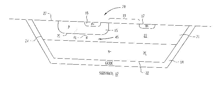
Figure 2 diagrammatically illustrates a first
embodiment of the present invention incorporated with a
dielectrically isolated island containing an NPN bipolar
transistor structure;
7zi

2033780
Figure 3 shows the incorporation of the embodiment of Figure
2 into an SOI architecture;
Figure 4 shows a modification of the embodiment of the
invention shown in Figure 2, in which the depth of the impurity
concentration-tailoring region is less than that of the base
region;
Figure 5 shows a second embodiment of the invention having a
deep semiconductor guard region contiguous with the base region;
Figure 6 is a sectional perimeter of a version of the second
embodiment of the invention having a deep guard region; and
Figure 7 shows a third embodiment of the invention, for
reducing the resistance of the drain-drift region of a DMOS
structure.
DETAILED DESCRIPTION
Referring now to Figure 2 a first embodiment of the present
invention is shown as comprising a bipolar (e.g. NPN) transistor
structure 20 formed within an (N type silicon) island region 21
dielectrically isolated from a (silicon) support substrate 12 by
means of an (oxide) insulator layer 14 at the bottom 22 and
sidewalls 24 of island region 21. (It should be noted that the
invention is not limited to a particular polarity type of device,
an NPN structure being shown and described merely as an example.)
As in the prior art configuration shown in Figure 1, discussed
above, transistor 20 contains a (P type) base region 15 disposed in
a first surface portion of N island region 21, such that the

2033780
semiconductor material of island region 21 extends beneath the
bottom 25 of base region 15 and thereby separates the bottom 25 of
the base region from the bottom 22 of the island region.
Support substrate 12 may surround dielectrically isolated
island 21, as shown in Figure 2, or it may be configured as a
semiconductor (silicon) on insulator architecture, diagrammatically
illustrated in Figure 3 as having a channel 31 of conductive (doped
polysilicon) material disposed adjacent to (the side surfaces of)
island region 21 and dielectrically isolated from both substrate 12
and island region 21 by insulator layer 34. Polysilicon channel 31
may be biased at a voltage different from that of substrate 12, so
that its bias does not influence that portion of island region 21
beneath base 15 (as the channel is not a boundary to that region).
As a consequence, the voltage applied to the polysilicon channel
need not be constrained.
NPN transistor 20 further includes an N+ emitter region 16
formed in a surface portion of base region 15, and an N+ collector
contact region 17 formed in a surface portion of the island region
spaced apart from base region 15 by a separation region 18
therebetween. In the embodiment illustrated in Figures 2 and 3, and
unlike the prior art architecture of Figure 1, an upper (N type)
portion 23 of island region 21, which extends from the top surface
27 of the island to a depth beneath the bottom 25 of base region
15, has an impurity concentration which is greater at its interface
with the base region than a lower (N- type) portion 26 adjacent to
the bottom 22 of the island. Region 23 may be formed (by ion

2033780
implant, diffusion) non-selectively, without the need for special
masking, or it may be selectively introduced into only specified
island regions within substrate 12, as required by a particular
design.
As described previously, this relatively higher impurity
concentration of upper portion 23 provides a low collector
resistance path through the (collector) island from a location 41
within the collectcr island beneath that portion of base region 15
which underlies emitter region 16 through the N type material of
the upper portion 23 of the island to collector contact region 17.
Normally, at a given collector voltage, this region of increased
doping would cause a higher electric field (resulting in a lower
BVCE0) in the base-collector depletion layer that is formed in the
portion 45 of island region 21 beneath base region 15 than would
occur in the absence of the increased doping. This unwanted
decrease in BVCE0 is obviated by biasing substrate 12 at a
potential, relative to the potential of the collector island region
21, such that, in the presence of a voltage bias differential
applied between the island (collector) region 21 and emitter region
16, that portion 45 of the collector island region 21 which extends
beneath base region 15 and separates the bottom 25 of the base from
the bottom 22 of the island region 21 becomes depleted of carriers
prior to the occurrence of a breakdown voltage field between the
collector island region 21 and emitter region 16. Namely, because
of the application of a substrate bias, that portion 41 of the
region 45 beneath the base becomes depleted of carriers, so that

2033780
its doping may be increased to a higher concentration than would be
possible in the absence of a substrate bias, while maintaining the
electric field at that location at less than the BVCE0 field. When
portion 45 of the collector island region 21 beneath base 15 is
fully depleted by the combined action of the substrate bias and
reverse base-collector junction bias prior to reaching the
breakdown field, the collector voltage may be increased further
until a breakdown field is reached in a lateral portion of the
base-collector junction (away from region 45).
As pointed out above, and as depicted in the embodiment of
Figures 2 and 3, the tailoring of the impurity concentration
profile of island region 21 for providing a reduced resistance path
between the base and the collector contact region 17 may be
s accomplished by introducing (ion implantation, diffusion)
impurities into the upper surface 27 of the island region 21, so
that higher (than the island) impurity concentration region 23
extends from the upper surface 27 of the island to a location some
defined distance deeper than the depth of base region 15, whereby
region 23 extends beneath the bottom 25 of the base region, yet
still leaving a lower N- portion 26 of increased resistivity
adjacent to the bottom 22 of island region 21.
This tailored doping may also extend completely through the
island region, so that the island region acquires a graded impurity
concentration profile decreasing from upper surface 27 and
extending to bottom 22 of island region. Again, the upper part of
the island will be more heavily doped, so that the lowest impurity

2033780
concentration of the collector island region occurs beneath the
bottom of the base region.
Where a lower reduction in collector resistance can be
tolerated as a tradeoff for purposes of gaining flexibility in
5 choice of island thickness for a given BVCEO, the depth of the
impurity concentration-tailoring region 23 may be relatively
shallow or less than that of base region 15, so that it terminates
at a side portion 51 of the base region, as illustrated in the
embodiment of Figure 4.
10In accordance with a second embodiment of the invention,
diagrammatically illustrated in Figure 5, reduced collector
resistance is achieved by forming a deep semiconductor guard region
61 of the same conductivity type as, contiguous with and having a
:. depth in collector island region 21 greater than that of base
15 region 15, so that the deep guard region 61 effectively interrupts
any surface path from that portion 41 of the collector island 21
underlying the emitter region 16 to collector contact region 17.
Substrate 12 is biased at a voltage which is less than the
collector voltage, such that the combined action of the base-
20 collector bias and the substrate bias depletes that portion 65 of
island region 21 between the bottom 63 of deep guard region 61 and
the bottom 22 of island region 21 of carriers prior to the
occurrence of a breakdown voltage field between the collector
island region and the base region. Once a depletion region has been
25 formed between the substrate and deep guard region 61, a further
increase in the base-collector voltage will cause little change in

2033780
the field underlying the emitter region 16 (namely within the
confines of the deep P type guard region, due to the screening
action of the depletion region. As a consequence, collector-to-
emitter voltage can be increased further, thereby achieving a
higher BVCE0 than would otherwise be obtainable in a collector of
the same doping and thickness.
To provide such a surrounding screen, deep guard region 61 may
be formed in the shape of a ring contiguous with the lateral
perimeter of the base, as indicated in Figure 5. It may also be
formed so as to be contiguous with one end of base region 15 and
extend across the width of the island region 21, so as to intersect
dielectric material 14 through which the island region is
dielectrically isolated from the substrate 12, as shown by the
sectional perspective illustration of Figure 6. Collector
resistance is kept low because thicker or more heavily doped
islands (which have lower collector resistance) can be used to
achieve the desired BVCE0 due to the deep P screening effect.
In addition, this second embodiment may be augmented by the
introduction of the impurity concentration-tailoring region 23,
described above. Preferably, N region 23 is no deeper than guard
region 61, as shown in broken lines in Figures 5 and 6, so that a
depletion region is formed between the guard region 61 and the
substrate 12 at the lowest possible voltage.
In accordance with a third embodiment of the invention, the
above-described impurity concentration-tailoring region may be
employed to reduce the resistance of the drain-drift region of a

2033780
DMOS structure, diagrammatically illustrated in Figure 7 as
comprising additional surface insulator and gate electrode
structure. More particularly, in the DMOS device shown in Figure 7,
N island region 21 acts as the drain, having an N+ surface drain
contact region 71. A channel-containing P type body region 72 is
formed in a surface portion of the island spaced apart from the
drain contact 71. An N+ source region 74 is formed in a surface
portion of body region 72 so as define the width of the channel
region 75 between the island 21 and the body region 72. Overlying
the channel is a thin gate insulator (oxide) layer 81. A layer of
gate conductor material (e.g. doped polysilicon, metal) 82 is
formed on the gate insulator layer and overlaps the source region
74 and island region 21, so as to extend over channel region 75.
As in the first two embodiments, a (drain drift) resistance-
reducing region 83 extends from the top surface 84 of the island to
! some defined distance deeper than the depth of the channel-
containing body region 72, so that it extends beneath the bottom 76
of the channel-containing body region and above the bottom 22 of
the lower impurity concentration island region. Again, the lowest
impurity concentration of the island region occurs beneath the
bottom of the body region. The support substrate is biased at a
voltage less than the drain voltage, so that the island region
between the body region and the underlying support substrate
becomes totally depleted of carriers before the breakdown field is
reached in that region.

2033780
In each of the foregoing embodiments, biasing of the substrate
12 may be accomplished by means of an ohmic contact to the
substrate or by a non-mechanical coupling mechanism, as long as the
substrate assumes a voltage less than the voltage of the collector
(island), so that the region between the base (or channel body in
the case of a DMOS device), and the substrate is fully depleted
before a breakdown field is reached. Such non-contact biasing of
the substrate may be effected by leakage current equalization (net
current to the substrate must be zero) or capacitive coupling.
Either technique will establish a substrate bias that is
intermediate the most negative and most positive voltages applied
to the integrated circuit.
As will be appreciated from the foregoing description of the
present invention, the considerable occupation area (and thickness)
of transistor structures that achieve low collector resistance by
means of a buried subcollector region at the bottom of the island
is substantially reduced by means of a thin dielectrically isolated
island structure, in which the impurity concentration of the
reduced thickness island region is tailored to provide a region of
reduced resistance for providing a low resistance current path from
an island location directly beneath the emitter region to the
collector contact. In addition, the potential of the support
substrate is established at a value which is less than the
collector voltage, so that the portion of the collector (island)
directly beneath the emitter projection onto the base is depleted
of carriers prior to the electric field at that location reaching

2033780
BVCEO, so as not to effectively reduce BVCEO. Since the support
substrate bias potential depletes some of the region of the island
beneath the base region of carriers, the doping of the island can
be increased compared to the case where the substrate is not
biased, while maintaining the electric field at this location less
than the BVCEO field.
While I have shown and described several embodiments in
accordance with the present invention, it is to be understood that
the same is not limited thereto but is susceptible to numerous
changes and modifications as known to a person skilled in the art,
and I therefore do not wish to be limited to the details shown and
described herein but intend to cover all such changes and
modifications as are obvious to one of ordinary skill in the art.
16

Dessin représentatif
Une figure unique qui représente un dessin illustrant l'invention.
États administratifs

2024-08-01 : Dans le cadre de la transition vers les Brevets de nouvelle génération (BNG), la base de données sur les brevets canadiens (BDBC) contient désormais un Historique d'événement plus détaillé, qui reproduit le Journal des événements de notre nouvelle solution interne.

Veuillez noter que les événements débutant par « Inactive : » se réfèrent à des événements qui ne sont plus utilisés dans notre nouvelle solution interne.

Pour une meilleure compréhension de l'état de la demande ou brevet qui figure sur cette page, la rubrique Mise en garde , et les descriptions de Brevet , Historique d'événement , Taxes périodiques et Historique des paiements devraient être consultées.

Historique d'événement

Description Date
Inactive : Demande ad hoc documentée 2018-08-16
Exigences relatives à la révocation de la nomination d'un agent - jugée conforme 2018-05-18
Exigences relatives à la nomination d'un agent - jugée conforme 2018-05-18
Inactive : CIB de MCD 2006-03-11
Le délai pour l'annulation est expiré 2004-01-08
Lettre envoyée 2003-01-08
Lettre envoyée 1999-01-21
Accordé par délivrance 1996-07-30
Demande publiée (accessible au public) 1991-07-09
Toutes les exigences pour l'examen - jugée conforme 1991-05-29
Exigences pour une requête d'examen - jugée conforme 1991-05-29

Historique d'abandonnement

Il n'y a pas d'historique d'abandonnement

Historique des taxes

Type de taxes Anniversaire Échéance Date payée
TM (brevet, 7e anniv.) - générale 1998-01-20 1997-12-31
TM (brevet, 8e anniv.) - générale 1999-01-08 1998-12-23
TM (brevet, 9e anniv.) - générale 2000-01-10 1999-01-06
TM (brevet, 10e anniv.) - générale 2001-01-08 2000-12-20
TM (brevet, 11e anniv.) - générale 2002-01-08 2001-12-20
Titulaires au dossier

Les titulaires actuels et antérieures au dossier sont affichés en ordre alphabétique.

Titulaires actuels au dossier
HARRIS CORPORATION
Titulaires antérieures au dossier
JAMES D. BEASOM
Les propriétaires antérieurs qui ne figurent pas dans la liste des « Propriétaires au dossier » apparaîtront dans d'autres documents au dossier.
Documents

Pour visionner les fichiers sélectionnés, entrer le code reCAPTCHA :


Pour visualiser une image, cliquer sur un lien dans la colonne description du document (Temporairement non-disponible). Pour télécharger l'image (les images), cliquer l'une ou plusieurs cases à cocher dans la première colonne et ensuite cliquer sur le bouton "Télécharger sélection en format PDF (archive Zip)" ou le bouton "Télécharger sélection (en un fichier PDF fusionné)".

Liste des documents de brevet publiés et non publiés sur la BDBC .

Si vous avez des difficultés à accéder au contenu, veuillez communiquer avec le Centre de services à la clientèle au 1-866-997-1936, ou envoyer un courriel au Centre de service à la clientèle de l'OPIC.

({010=Tous les documents, 020=Au moment du dépôt, 030=Au moment de la mise à la disponibilité du public, 040=À la délivrance, 050=Examen, 060=Correspondance reçue, 070=Divers, 080=Correspondance envoyée, 090=Paiement})


Description du
Document 
Date
(aaaa-mm-jj) 
Nombre de pages   Taille de l'image (Ko) 
Revendications 1996-07-29 49 1 820
Description 1996-07-29 51 1 855
Dessins 1996-07-29 7 83
Revendications 1994-02-25 9 275
Dessins 1994-02-25 7 84
Description 1994-02-25 16 563
Abrégé 1994-02-25 1 26
Abrégé 1996-07-29 1 30
Dessin représentatif 1999-07-18 1 7
Avis concernant la taxe de maintien 2003-02-04 1 174
Taxes 1997-12-30 1 49
Correspondance 1999-01-20 2 61
Taxes 1995-12-28 1 30
Taxes 1997-01-05 1 34
Taxes 1993-12-20 1 27
Taxes 1994-12-21 1 35
Taxes 1992-12-08 1 22
Courtoisie - Lettre du bureau 1991-07-28 1 21
Correspondance de la poursuite 1996-03-06 1 27
Courtoisie - Lettre du bureau 1996-06-02 1 69
Correspondance de la poursuite 1996-05-06 1 47
Correspondance de la poursuite 1995-07-12 2 69
Demande de l'examinateur 1995-04-12 2 89
Correspondance de la poursuite 1993-05-19 1 31
Demande de l'examinateur 1993-03-03 1 52
Correspondance de la poursuite 1991-01-07 60 1 950
Correspondance de la poursuite 1991-05-28 1 31