Note : Les descriptions sont présentées dans la langue officielle dans laquelle elles ont été soumises.
~035~.8
BACRGROUND OF TH~ INVENTION
The invention involves a chip carrier for a microwave
semiconductor component wherein four external electrical contacts
are provided including two external source terminals, one external
gate terminal, and one external draln ter~inal.
A chip carrier for microwave semiconductor components is for the
purpose of permitting an encapsulation of the microwave
semiconductor components which is suitable above 12GHz, thereby
preserving microwave-properties of the semiconductor component.
The carrier also serves the purpose of maintaining stability
(vibration prevention) and simultaneously largely suppressing
feedback, overcoupling, and undefined impedances.
A chip carrier should be suitable for surface-mountable microwave
semiconductor components.
A chip carrier should permit a favorable phase performance Sll
as well as a favorable reaction behavior S12, and have small
housing losses.
Even when a plastic housing is used, a chip carrier premits at
least the same favorable properties as are achieved with a
microwave semiconductor component in a ceramic housing.
8UMMARY OF~HE INVENTION
The present invention is based on the object of specifying a chip
carrier of the initially described type which permits favorable
operating and application behavior, even when a plastic housing is
used.
According to the invention, a chip carrier has at least first and
second external source terminals, an external drain terminal, and
an external source terminal. A first of the four source terminals
and the external drain terminal are arranged on a first side of the
20352~8
chip carrier and a second of the source terminal and an external
gate terminal are arranged on a second opposite side of the chip
carrier. With respect to a geometric line running in a plan view
across the chip carrier, the first external source terminal and the
external drain terminal are on one side of the geometric line and
the second external source terminal and the external gate terminal
are on a second opposite side of the chip carrier. The first
external source terminal and the second external source terminal
are located on different sides of the geometric line. The first
external source terminal is connected with the second external
source terminal as one piece via a cross member. A region on the
cross member is provided for fastening the semiconductor chip
thereon. The cross member substantially proceeds obliquely
relative to the geometric line.
The invention permits considerable improvements in the phase
performance S11 as well as in the reaction behavior S12, and
provides for low housing losses. The invention also permits the
use of a plastic housing even above 12GHz, thus permitting an
operating and application behavior which can be achieved with a
microwave semiconductor component in a ceramic housing, e.g. a
CEREC-70.
A chip carrier according to the invention is particularly
suitable for SMD (Surface mounted device) components. A chip
carrier according to the invention is particularly suitable for a
SOT143-component. A chip carrier according to the invention is in
particular also suitable for a Mini-SOT-component.
A chip carrier according to the invention is suitable for the
broadband matching circuits that are standard for CEREC-70-
housings.
A chip carrier according to the invention can be designed such
that it is PIN-compatible to the CEREC-70 housing.
~035~8
A chlp carrier according to the invention is particularly
suitable for a HEMT (High electron mobility transistor) component.
A chip carrier according to the invention is also suitable for
other microwave components.
A chip carrier according to the invention resul~s in a microwave
component which reacts in an insensitive manner to user circuits,
particularly to source-groundings, as they are provided by
different pc board materials.
The diagonal ground cross member between the two external source
electrodes permits, in the case of a chip carrier according to the
invention, the shortest possible gate connection to the outside
given the simultaneous accommodation of the source terminals. The
geometric and electrical length between the external gate terminal
and the semiconductor chip is advantageously reduced to a minimum.
The gate terminals of the semiconductor chip are advantageously
contacted in optimally short fashion, and if possible also in
double contacted fashion. The source terminal of the semiconductor
chlp is advantageously contacted in a four-fold fashion, and
likewise is contacted with optimally short bond wires. The gate
electrode of the chip carrier is advantageously widened. An
anchoring of the gate electrode and/or the drain electrode of the
chip carrier in a plastic cover of the component by means of a hook
and/or at least one breakthrough are advantageously designed such
that there are no disadvantageous electrical effects.
The source negative feedback due to the cross member or web in
the housing is low due to the low dielectric constant of the
plastic material of the cover of the component. The inner coupling
of the gate terminal and of the drain terminal of the component via
the source cross member to the end capacitances that are low
themselves is thus likewise low.
203~2~1.8
Advantageously, the gate electrode i~ cut in oblique fashion
where it is directly adjacent to the cross member. Thus, a shorter
running time of the microwaves results.
Advantageously, the gate electrode is cut in oblique fashion
where it is directly ad;acent to the cross member. Thus, a shorter
running time of the microwaves results.
Advantageously, the gate electrode is as closely adjacent to the
cross member as possible. Thus, snd capacities, scattering, and
tolerances for cutting tools must be taken into account, however.
A parameter for a very small distance between the gate electrode
and the cross member which, according to findings to date is
appropriate, is approximately O.l mm.
The external contacts of the chip carrier advantageously are at
an operating distance that is useful for the user so that no solder
bridges between ad~acent external contacts develop. A suitable
parameter for such a distance between two adjacent external
contacts is, for example, 0.6 mm. Given an increasing
miniaturization, these distances between adjacent external contacts
can be decreased.
A mini-SOT-housing has a shorter plastic body than a SOT143-
housing (in longitudinal direction). Even for such a plastic body,
a chip carrier according to the invention can be used.
When the semiconductor chip is placed obliquely to the
longitudinal axis or the transverse axis of the chip carrier, the
path from the gate electrode to the semiconductor chip gate
terminal can be shortened. Thus, a shorter length of the
contacting wires is possible.
A component with a chip carrier according to the invention is
user-friendly and permits a low phase rotation from the external
gate terminal and drain terminal to the semiconductor chi~.
;~03~i%~.8
In a simple manner, a chip carrier according to the invention
permits a four-fold contacting between the semiconductor chip and
the source electrode. A chip carrier according to the invention
permits in a simple manner a two-fold contacting between the
semiconductor chip and the drain electrode. A chip carrier
according to the invention permits in a simple manner a two-fold
contacting between semiconductor chip and gate electrode.
A chip carrier according to the invention gives better results
for a HEMT than a ceramic housing. In adaptability, a chip carrier
according to the invention can be at least compared to a ceramic
housing .
Advantageously, the external gate terminal is wider than the
external drain terminal. A Pavorable value for the width of the
external gate terminal lies between approximately 0.5 mm and 0.8
mm.
Advantageously, the drain electrode is arranged as close to the
cross member as possible in the direction toward the semiconductor
chip. Thus, short contacting wires and a short path for the
microwaves are provided.
The drain electrode can be contacted in single or double fashion.
The gate electrode can be contacted in single, double, or four-fold
fashion. The source electrode can be contacted in single, double,
or four-fold fashion.
The connection between the semiconductor chip and the gate
electrode is advantageously as short as possible. The connection
between the semiconductor chip and the gate electrode is
advantageously guided in low-ohmic fashion according to the wave
impedance to the external housing terminal.
For the anchoring of the gate electrode or the drain electrode
in a covering for the microwave component to be applied at a later
time, advantageously noses and/or breakthroughs in the respective
;~0352~
electrodes are provided. From this results a good mechanically
stab]e anchoring of these electrodes in the plastic body of the
component.
A microwave component with a chip carrier according to the
invention is SMD-capable. Such a SMD-microwave component with such
a SMD-housing fulfills microwaYe properties at least in a
satisfactory manner.
The different terminals (pads) on the semiconductor chip for
source, drain, and gate can be arranged on this semiconductor chip
in any way. Thus, even given a straight arrangement of the
semiconductor chip relative to the longitudinal axis or the
transversa axis of the chip carrier, favorable microwave properties
are achieved.
A microwave component with a chip carrier according to the
invention has favorable four-pole-S-parameters. A microwave
component with a chip carrier according to the invention has a
small phase rotation at S11. A microwave component with a chip
carrier according to the invention has a phase of almost 180.
Advantageously, the semiconductor chip is arranged on the cross
member as clo3e as possible to the gate electrode.
BRIEF_~E8QRIPTION OF_TH9 DRAWINGB
Figures l to 7 explain various embodiments of a chip carrier
according to the invention, or of a microwave component with a chip
carrier according to the invention:
Figure 8 shows a SMD-microwave component with a chip carrier
according to the invention;
Figure 9 shows phase behavior Sll of a micxowave component with
a chip carrier according to the invention; and
Figure lo shows the four-pole-S-parameters for a microwave
component with a chip carrier according to the invention.
;~0352~.~
DESCRIPTION OF THE PREFERRED EMBODIMEN~
Figures 1 to 7 explain various chip carriers or microwave
components with a chip carrier. The same parts are thus provided
with the same reference symbols. In the drawing, only chip
carriers with four external electrical terminals are shown. The
invention is also suitable, however, for chip carriers with more
than four external electrical terminals, e.g. for a MMIC-microwave
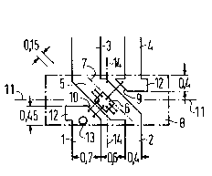
component. A chip carrier according to the drawing has one
external gate terminal 1, two external source terminals 2, 3 and
one external drain terminal 4. The external gate terminal 1 and
one external source terminal 2 are alongside of the chip carrier.
The other external source terminal 3 and the external drain
terminal 4 are located on an opposite side of the chip carrier.
The chip carrier has a longitudinal axis 11 and a transverse axis
14. The two external source terminals 2, 3 are located on opposite
sides of the longitudinal axis 11 as well as on opposite sides of
the transverse axis 14. The axis 14 of the chip carrier defines
a geometric line proceedlng on one side of the carrier between the
external gate terminal 1 and the external source terminal 2 and,
on the opposite side of the chip carrier, between the other
external source terminal 3 and the external drain terminal 4. The
two external source terminals 2, 3 are connected as one piece via
the cross member 5. The cross member 5 basically proceeds
obliquely to the axis (geometric line) 14. Within the cross member
5, a center line can be defined which connects the center line of
the external source terminal 2 with the center line of the external
source terminal 3. This center line 7 within the cross member 5
basically proceeds ohliquely to the axis (geometric line) 14. It
is favorable when the cross member 5 proceeds essentially at an
angle of 45 to the axis (geometric line) 14. The contacting wires
~035X~.8
between the semiconductor chip 6 and the gate electrode are to be
as short as possible. For this reason, the gate electrode has an
obllque ~order 10 where it i~ the most closely ad~acent to the
cross member 5. This oblique bordering 10 favorably proceeds
likewlse at an angle of 45 to the axis (geometrical line) 14. The
semiconductor chip 6 is likewise arranged in oblique fashion
relative to the axis (geometrical line) 14. The semiconductor chip
6 is as closely adjacent to the gate electrode as possible. The
axes of the semiconductor chip are at an angle of 45 to the axis
(geometric line) 14. Also the drain electrode is closely adjacent
to the cross member 5. The drain electrode, too, has a border 9
where it is most closely adjacent to the cross member, this border
proceeding obliquely to the axis (geometric line) 14.
A microwave component with a chip carrier is provided with a
covering 8. The covering 8 can correspond to the covering of a
SOT143-housing. When the covering 8 corresponding to the covering
of a SOT143-housing is shortened on both ends (relative to the axis
11), one obtains the covering of a mini-SOT housing.
The external gate terminal 1 is constructed wider than the
external drain terminal 4. In order to permit a mechanically
stable anchoring of the chip carrier in the covering 8, and in
order to avoid electrical disadvantages, the gate electrode has a
breakthrough 13 and a nose 12, and the drain electrode also has a
nose 12.
In the exemplary embodiment, the external gate terminal 1 has a
width of 0.7 mm and the external drain terminal 4 has a width of
0.4 mm. The external gate terminal 1 has a distance to the
external source terminal 2 of 0.6 mm. The gate electrode has a
distance to the cross member 5 along the border 10 of 0.15 mm. The
border of the gate electrode adjacent to the axis 11 has a distance
.8
of 0.45 mm to the border of the covering 8. The border of the
drain electrode that is most closely adjacent to the axis 11 has
a distance of 0.4 mm to the edge of the covering 8.
Figure 4 shows a chip carrier whereby the borders of the gate
electrode, the drain electrode, and of the cross member 5 have been
optimized. Thus, it is not necessary that the opposite borders of
the cross member 5, for example, proceed in parallel fashion to one
another. It suffices when the cross member 5 proceeds basically
obliquely to the axis (geometric line) 14.
Eigure 5 ~hows a microwave component with a chip carrier whereby
the semiconductor ~hip 6 is arranged such that its edges proceed
in parallel fashion to the axes 11, 14. Such a microwave component
is useful, for example, for an application at 8GHz. For an
application at higher frequencies, e.g. at 12GHz, an oblique
arrangement of the semiconductor chip 6 relative to the axes 11,
14 according to figure 6 is to be preferred.
Figure 7 shows a microwave component with a chip carrier whereby
the semiconductor chip 6 is arranged in oblique fashion relative
to the axes 11, 14. The semiconductor chip 6 is contacted in
double fashion with the gate electrode, in double fashion with the
drain electrode, and in four-fold fashion with the source
electrode.
A comparison of figure 4 with figure 7 shows that in the case of
a microwave component according to figure 4, the contacting wires
between the gate electrode and the semiconductor chip 6, and
between the semiconductor chip 6 and the drain electrode, are
shorter than in the case of a microwave component according to
figure 7.
Figure 8 shows the outside dimensions of a 12GHz-GaAs-microwave
component in a SMD-plastic housing. When used for a HEMT given a
frequency of 12 GHz, a voltage VDS of 2V, and a current ID of 12mA
;~03SX~.8
one obtains a noise factor F/dB/type of 1.3 and a gain at noise
matching Gass/d~/type of 10.5. Using a microwave component with
a chip carrier for a GaAs-field effect transistor given a frequency
of 12GHz, a voltage VDS of 3V, and a current ID of 15mA results in
a noise factor F/dB/type of 1.8 and a gain at noise matching
Gass/dB/type of 8.5.
Figure g shows the phase performance Sll of a microwave component
with a chip carrier with a plastic cover in a SOT143-housing at a
frequency of 12GHz. There, the semiconductor chip is contacted in
four-fold fashion with the source electrode. The point shows the
value for the phase performance S11 given a single contacting o~
the semiconductor chip with the gate electrode. The cross shows
the value for the phase performance Sll given a double contacting
of the semiconductor chip with the gate electrode.
Figure 10 shows the different four-pole-S-parameters for a
microwave component with a chip carrier whereby a HEMT as the
semiconductor chip is contacted in four-fold fashion with the
source electrode, in double fashion with the drain electrode, and
in double fashion with the gate electrode. The marking with the
number 4 thereby corresponds to a frequency of 12GHz.
~ chip carrier according to the invention can be modified in many
ways. For example, the entire chip carrier can be laterally
reversed relative to the axis 11. Then, the external terminals 1
and 3, and the external terminals 2 and 4, are respectively
exchanged with one another. For example, the entire chip carrier
can be laterally reversed relative to the axis 14. Then, the
external terminals 1 and 2 and the external terminals 3 and 4 are
respectively exchanged with one another. Also, the borders of the
cross member 5, and/or the gate electrode 15, and/or the drain
electrode 16 can be varied, for example.
11
~035~.8
Although various minor changes and modifications might be
proposed by those skilled in the art, it will be understood that
I wish to include within the claims of the patent warranted hereon
all such changes and modifications as reasonably come within my
contribution to the art.