Note : Les descriptions sont présentées dans la langue officielle dans laquelle elles ont été soumises.
CA 02035222 1998-OS-06
-1-
BACKGROUND AND SUMMARY
The invention relates to disconnect switches
for use with the start or auxiliary winding of a
capacitor-start capacitor-run single phase AC induction
motor.
The invention relates to continuing
development efforts and improvements over the circuitry
shown in Bossi et al U.S. Patent 4,782,278, assigned to
the assignee of the present invention. The
invention also arose from
continuing development efforts relating to U.S. Patents
4,604,563, 4,622,506, 4,658,195, 4,687,982, 4,670,697;
4,745,347, 4,751,449; 4,751,450, 4,782,278 and
4,786,850, also assigned to the_assignee of the present
invention.
A capacitor-start capacitor-run single phase
AC induction motor is subject to a phenomenon known as
"first cycle current spiking", and to another
phenomenon known as "cycle to cycle current spiking".
The first cycle current spiking is experienced in both
mechanical and solid state disconnect switches.
The present invention addresses and solves
the first cycle current spiking problem, and also
addresses and solves the cycle to cycle current spiking
problem.
As is known in the prior art, a single phase
AC induction motor has a main winding and an auxiliary
winding both connectable to an AC power source. A
start capacitor provides a phase shifted field for
starting torque. A semiconductor power switch
automatically connects and disconnects the start
capacitor to and from the AC source in starting and
running modes, respectively. The gate current for the
semiconductor power switch is derived through a
resistor, such as resistor 72 in the above noted Bossi
- 2 --
~~Ji~iv:~
et al patent, connected to a node common to the start
capacitor and a main terminal of the power switch.
This circuitry performs admirably on capacitor start or
split phase motors. However, when applied to
capacitor-start capacitor-run motors, a gate circuit of
this type is subject to the above noted first cycle
current spiking and cycle to cycle current spiking.
One solution to current spiking known in the
prior art is to provide a choke for the run capacitor, '
such as a large inductance or coil connected in series
with the run capacitor or an extended winding. The
choke is undesirable because it is massive and
expensive., Furthermore, the choke does riot solve the
first cycle current spiking problem. The choke does
reduce the current spike, but not enough to be
satisfactory. Another disadvantage of the choke is '
that it requires the insertion of an element in series
with the run capacitor, which is costly from a
manufacturing standpoint. Another disadvantage of the
choke is that it is in the circuit continuously.
The present invention provides a solution
which is particularly simple and effective, and
eliminates the need for a separate series connected
choke.
The present invention solves the first cycle
current spiking problem by controlling when, in
relation to the AC cycle, the power switch is allowed
to turn on, rather than just allowing the power switch
to turn on at random-~=during any point in the AC cycle
upon initiation of the starting mode. Instead, the
start switch may be turned on only within a known or
predictable range of voltage differential between the
run and start capacitors.
The present invention solves the cycle to
cycle current spiking problem by controlling phasing of
a:~~Ji~~~.,
gate current to the start switch to be in phase with
the voltage across the run capacitor and out of phase
with the current through the series connected start
switch and start capacitor.
BRIEF DESCRIPTION OF THE DRAWINGS
FIG. 1 schematically shows a typical
environment in which the preferred embodiment of the
present invention is used.
FIG. 2 is a circuit diagram illustrating
circuitry constructed in accordance with the invention.
FIG. 3 is a waveform diagram illustrating
operation of the invention..
DETAILED DESCRIPTION
As known in the prior art, a single phase AC
induction motor has a main winding for running the
motor, and a start or auxiliary winding together with
the run winding for starting the motor. The start
circuit is energized when starting the motor from rest
and then disconnected at a given motor speed. The
fields in the main and auxiliary windings are phase
shifted, for example by capacitance, inductance,
resistance or the like, to establish a rotating
magnetic field for starting and/or running torque.
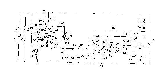
FIG. 1 shows a main winding 1 and auxiliary
winding 2 connectable through a main switch 3 to an AC
power source 4. Capacitors 5 and 7 provide the phase
shift for starting torque. When the motor reaches a
given threshold cut-out speed, switch 6 is opened to
disconnect start capacitor 5 from AC power source 4.
Capacitor 7 is a run~capacitor and provides phase shift
for running torque.
FIG. 2 shows circuitry for controlling start
switch 6. A main voltage detector circuit including
diode 10 is connected across AC source 4 for sensing
the input AC line reference voltage. Voltage from AC
~~~52~~
-4-
source 4 is sensed through resistor 12 and half wave
rectifying diode 10, and filtered by a capacitor 14.
Varistor 16 provides transient spike protection. An
NPN bipolar pass transistor 18 has its emitter-
collector circuit connected between the cathode of
diode 10 and node 19 which provides a DC power supply
for a pair of comparators 20 and 22, to be described.
The base circuit of transistor 18 includes a zener
diode 24 applying a limited voltage from AC source 4
through diode 10 to the base of transistor 18 to bias
the latter into conduction. Base drive current is
supplied through resistor 26.
An auxiliary voltage detector circuit
including diode 30 is connected across auxiliary
winding 2 for sensing auxiliary winding voltage. The
auxiliary winding voltage is reduced by the voltage
divider network provided by resistors 32 and 34 and
sensed through half wave rectifying diode 30 and
resistor 36 and filtered by capacitor 38, to provide
sensed auxiliary winding voltage at node 40.
Voltage comparators 20 and 22 are provided by
a dual comparator integrated circuit, provided by an
LM393 integrated circuit, where manufacturer assigned
pin number designations are shown to facilitate
understanding, having power supply voltage provided at
line 42 from node 19, and are connected by line 44 to a
common reference at ~~. Non-inverting input 46~ of
comparator 20 senses voltage from AC source 4 at node
48 as reduced by the voltage divider network provided
by resistors 50 and 52 from line 49 connected to the
cathode of diode 10, to provide floating line
compensation. inverting input 54 of comparator 20
senses auxiliary winding voltage at node 40.
Comparator 20 compares the auxiliary winding voltage
against the voltage from AC source 4. When the
CA 02035222 1998-OS-06
-5-
auxiliary winding voltage increases as a function of
motor speed to a predetermined cut-out value relative
to the voltage at node 48 from AC source 4, comparator
20 outputs a turn-off signal at output 56 causing
switch 6 to open and disconnect start capacitor 5 from
AC source 4, to be described. When the auxiliary
winding voltage decreases as a function of motor speed
to a predetermined cut-in value relative to the voltage
at node 48, comparator 20 outputs a turn-on signal at
output 56 causing switch 6 to close and connect start
capacitor 5 to AC source 4. The predetermined cut-in
value corresponds to a voltage derived from
rotationally induced voltage in the auxiliary winding
during overload or stall of the motor after starting.
At initial energization of the motor, the
scaled down auxiliary winding voltage at node 40 is
substantially smaller than the scaled down main winding
voltage at node 48, and hence the voltage at comparator
input 54 is less than that at comparator input 46, and
thus comparator output 56 is high, as referenced
through pull-up resistor 57 to node 19. Comparator
output 56 is connected to inverting input S8 of
comparator 22. When comparator output 56 is high,
comparator output 62 is low, which enables conduction
from node 19 through resistor 64 and light emitting
diode 66, which turns on switch 6 if certain conditions
are met, to be described.
Switch 6 is an optically triggered
semiconductor power switch, including a power triac 68,
a pilot triac 69, and ~a light responsive elenent
provided by a light responsive triac 71. LED 66 and
light responsive element 71 are provided by a P9otorola
MOC3063*integrated circuit, and manufacturer assigned
pin number designations are shown to facilitate
understanding. LED 66 and light responsive element 71
* trade-mark
' 6' ~~:3;~~~,
may alternatively be provided by a Siemens IL410
integrated circuit, or the equivalent. LED 66 is
optically coupled to light responsive element 71 to
optically drive the latter into conduction if the
voltage thereacross at pins 4 and 6, at respective
terminals 100 and 108, is below a given maximum
level. Conduction of light responsive element 71
supplies gate current to pilot triac 69 to trigger the
latter into conduction which in turn supplies gate
current to triac 68 to trigger the latter into
conduction. Upon conduction of triac 68, current flows
from AC source 4 through start capacitor 5 and combines
with the run capacitor current through auxiliary
wind ing 2 .
As motor speed increases, the sensed
auxiliary winding voltage at node 40 increases. At a
given cut-out value, the voltage at comparator input 54
increases as a function of motor speed above that at
comparator input 46. Comparator output 56 then goes
low, which low state is supplied to comparator input
58, which in turn causes comparator output 62 to go
high. The high state at comparator output 62 disables
conduction through LED 66, which terminates the
emission of light to light responsive element 71 such
that the latter turns off, which in turn removes the
gate drive from pilot triac 69 and power triac 68, such
that the latter turns~~_off. Turn-off of triac 6.8
disconnects start capacitor 5 from AC source 4.
Comparator output 56 is connected through
resistor 80 to comparator input 46 at node 48. When
comparator output 56 goes low at the noted cut-out
speed, the voltage at comparator input 46 is reduced
through the connection provided by resistor 80, i.e.
the voltage at input 46 is pulled low by its connection
through resistor 80 to low output 56. Output 56 is now
~~~J~~~
_?_
at approximately the same potential as reference 53.
The voltage at comparator input 46 is modified because
resistor 80 is now effectively in parallel with
resistor 52. Comparator output 56 will not transition
high again until the auxiliary winding voltage at input
54 decreases below the lowered and modified selected
reference voltage at input 46. Comparator output 56
then goes high again, to turn on start switch 6, under
given conditions to be described, and reconnect start
capacitor 5 to AC source 4. The connection through
resistor 80 provides hysteresis such that the cut-in
speed is always lower than the cut-out speed.
The connection through resistor 80 changes
the voltage at comparator input 46 according to the
voltage at comparator output 56 such that the auxiliary
winding voltage at comparator input 54 is compared
against different voltages at comparator input 46. A
lower comparison reference voltage is provided at input
46 when output 56 is low and outputting a turn-off
signal because resistor 80 is now effectively in
parallel with resistor 52. A higher comparison
reference voltage is provided at input 46 when output
56 is high and providing a turn-on signal. Auxiliary
winding voltage must decrease to a cut-in value
established by the new voltage divider ratio of
resistors 50, 52 and 80 which is less than the cut-out
value, whereupon comyarator output 56 changes states to
output a turn-on signal to comparator 22 to reconnect
start capacitor 5 to AC source 4.
Resistor 80 is connected between comparator
inputs 58 and 60 and provides a voltage drop
therebetween. Comparator input 60 is connected to node
48. When comparator output 56 is low, the voltage from
AC source 4 at node 48 is dropped across resistor 80 in
parallel with resistor 52 to low output 56, and the
~~35~M~
_$_
voltage at comparator input 60 is higher than that at
comparator input 58. When comparator output 56 is
high, the voltage at output 56 is dropped across
resistor 80 to node 48 and through resistor 52 to
common reference 53, and the voltage at comparator
input 58 is higher than that at comparator input 60.
Run capacitor 7 has first and second
terminals 86 and 88. Start capacitor 5 has first and
second terminals 90 and 92. Terminals 88 and 92 are
connected to each other at a common node 94 at terminal
T4. Start winding 2 has one side connected to termina l
T4 at node 94 and the other side connected to AC source
4 at terminal T1. Terminal 86 of run capacitor 7 is
connected at terminal T2 to the first main terminal 96
of power triac 68. Terminal 90 of start capacitor 5 is
connected at terminal T3 to the second main terminal 98
of power triac 68. Light responsive element 71 has a
first main terminal 100 connected through gate terminal
102 and main terminal 104 of pilot triac 69 to gate
terminal 106 of power triac 68. Light responsive
element 71 has a second terminal 108 connected to node
110. Resistor 112 has a first terminal 114 connected
at node 116 to terminal 90 of start capacitor 5 and to
main terminal 98 of power traic 68. Resistor 112 has a
second terminal 118 connected at node 110 to terminal
108 of light responsive element 71 and to main terminal
120 of pilot traic 6~- Resistor 122 has a first
terminal 124 connected to node 110, and a second
terminal 126 connected to node 94 common to terminals
88 and 92 of run and start capacitors 7 and 5.
Resistor 128 is connected between gate terminal 106 and
main terminal 96 for providing improved dv/dt
capability of power triac 68, as known in the art.
Resistor 130 is connected between gate terminal 102 and
main terminal 104 for providing improved dv/dt
capability of pilot triac 69, as known in the art.
_g_
~~J~~~
The capacitor-start capacitor-run single
phase AC induction motor thus has a main winding 1 and
an auxiliary winding 2 connected to an AC power source
4, a run capacitor 7 for providing a phase shifted
field for starting and running torque, a start
capacitor 5 for providing a phase shifted field for
starting torque, a start switch 6 for automatically
connecting and disconnecting start capacitor 5 to and
from AC source 4 in starting and running modes,
respectively. Run capacitor 7 and start capacitor 5
are connected in parallel in the starting mode such
that during the first cycle of AC source 4 upon
initiation of the starting mode, there is an .
equalization of capacitor voltages if there is charge
remaining on the capacitors from the previous running
mode. Due to this equalization of capacitor voltages,
there is an exchange of current between capacitors 7
and 5, resulting in current flow through the loop
including capacitors 7 and 5 and start switch 6. This
current flow may reach a high peak current spike if
there is a large magnitude voltage differential between
capacitors 7 and 5. If uncontrolled, this current
exchange and the resulting potential high peak current
spike can damage start switch 6 and/or start capacitor
5. As noted above, prior solutions include the
provision of a choke such as a large coil or inductance
in series with run capacitor 7, or an extended winding
thereof.
The present invention provides a simple,
inexpensive solution to the noted first cycle current
spike problem. Light responsive element 71 provides an
inhibit switch responsive to the magnitude of the
voltage differential between run capacitor 7 and start
capacitor 5 and preventing start switch 6 from
connecting start capacitor 5 to AC source 4 until such
-7.0-
A~0352F~
magnitude drops below a given maximum level, to reduce
the first cycle current spike and reduce damage to and
extend the life of start switch 6 and start capacitor
5.
In typical applications, at initial
application of power to the motor, start capacitor 5
may have a residual charge of 150 to 200 volts if the
motor was immediately re-energized after it was
previously energized, while run capacitor 7 may be at
an equal voltage of opposite polarity at the moment
start switch triac 6 turns on. The resulting current
spike under these conditions due to the noted voltage
differential and current exchange, referred to w s the
first cycle current spike, may theoretically reach
1,000 plus peak amperes. A current spike of this
magnitude may be nearly instantly destructive to triac
6 due to the severe di/dt stress. This problem is
solved by the present invention.
The gate circuit of power triac 68 is
connected through light responsive element 71 to the '
loop containing run and start capacitors 7 and 5 to
derive gate current therefrom for gating power triac 68
as controlled by light responsive element 71.
Conduction of light responsive element 71 is controlled
by light emitting element 66 when the voltage across
light responsive element 71, i.e. across terminals 100
and 108, is below a predetermined value. When the
voltage across light responsive element 71 is above the
predetermined value, light responsive element 71 cannot
be optically triggered into conduction, which in turn
prevents gate current flow to pilot triac 69 and power
triac 68, to prevent conduction of power triac 68, and
hence prevent connection of start capacitor 5 to AC
source 4 regardless of the condition of light emitting
element 66.
~~3~~~~
-11-
Terminal 108 of light responsive element 71
is connected through resistor 112 to start capacitor
terminal 90. Terminal 100 of light responsive element
71 is connected through gate terminal 102 of pilot
triac 69, main terminal 104 of pilot triac 69, gate
terminal 106 of power triac 68, and main terminal 96 of
power triac 68 to terminal 86 of run capacitor 7.
Resistors 112 and 122 form a voltage divider network
which provides a voltage level at terminal 108 of light
responsive element 7I proportional to the magnitude of
voltage across start capacitor 5. Thus, light
responsive element 71 detects the difference in voltage
between terminal 86 of run capacitor 7 and terminal 90
of start capacitor 5. If the magnitude of the voltage
differential is greater than the noted given maximum
level, then light responsive element 71 will remain
nonconductive and in an inhibit mode until such time
that the voltage differential drops below such level,
at which time light responsive element 71 will become
conductive if still receiving light from light emitting
element 66, which in turn permits gate current flow
through gate terminal 102 which triggers pilot triac 69
into conduction which in turn permits gate current flow
through gate terminal 106 to trigger power triac 68
into conduction. Hence, turn-on of power triac 68 is
accomplished within a known or predictable range of
voltage differential='bf run and start capacitors 7 and
5.
The invention also provides a simple,
inexpensive solution to the noted cycle to cycle
current spike problem. After initial turn-on during
the noted first cycle, power triac 68 needs to be
triggered into conduction by gate current from the gate
circuit during each half cycle of the AC source
following a zero-crossing of current through triac
-12- ~~35~Mw
68. In the prior art, it is typical to derive gate
current through a resistor, such as resistor 72 in the
noted Bossi et al patent, connected to a node common to
the start switch and the start capacitor. This allows
the use of a low wattage series limiting resistor such
as 72 in Bossi et al because, assuming that the LED 66
is illuminated sufficiently to allow conduction of the
light responsive element, as soon as sufficient current
flows through resistor 72 to the gate of triac 68, the
triac will switch to a conductive state and limit the
voltage drop across resistor 72 to a low value. Gate
dissipation of triac 68 is also minimized with this
approach. This type of circuitry performs admirably on
capacitor-start or split phase motors. However, when
applied to capacitor-start capacitor-run motors, such
circuitry results in the above noted phenomenon of
cycle to cycle current spiking. This is because a
voltage differential between run and start capacitors 7
and 5 provides a potential voltage source for driving
current spikes in the loop including run capacitor 7,
triac 68 and start capacitor 5, without any inductance
or significant resistance to slow current rise. In
contrast, in a capacitor-start motor, without run
capacitor 7, the only remaining loop through triac 68
and start capacitor 5 includes auxiliary winding 2,
which provides an inductance for modifying the rate of
change of current, fi5r reducing the rate of current
rise.
In capacitor-start capacitor-run single phase
AC induction motors, there is no inductance in the loop
including run capacitor 7, triac 68 and start capacitor
5, and hence even a small voltage differential between
run capacitor 7 and start capacitor 5 will produce high
current. As above noted, one solution known in the
prior art to prevent such high current is to provide a
-13- i~~a~Ji~~.:i~
choke or inductance in series with run.capacitor 7 to
retard such current flow. The present invention
provides a simpler solution to the cycle to cycle
current spike problem, without the expense of a choke
or inductance.
During the starting mode, the voltage across
run capacitor 7, as shown at waveform 140 in FIG. 3, is
in phase with the voltage across start capacitor 5, as
shown at waveform 142. The current through the series
connected triac 68 and start capacitor 5, as shown at
waveform 144, is 90° out of phase with the voltage
across run capacitor 7. In the present invention, gate
current, as shown at waveform 146 in FIG. 3, is
supplied to the gate circuit of triac 68 in phase with
the voltage 140 across run capacitor 7, and 90° out of
phase with the current 144 through the series connected
triac 68 and start capacitor S. This is desirable
because substantially maximum gate current is supplied
to gate terminal 106 of triac 68 at zero-crossing 148
of current 144 through triac 68 and at substantially
maximum voltage 140 from the AC source across run
capacitor 7. This minimizes turn-on delay of triac 68
following the zero-crossing, to minimize the magnitude
of cycle to cycle current spikes and di/dt stress of
triac 68 and start capacitor 5.
In contrast, if the gate current supplied to
triac 68 is in phase=iJith the current through the
series connected triac 68 and start capacitor 5, then
there will be a delay in turn-on of triac 68 following
the zero-crossing of current therethrough until the
gate current which is in phase therewith rises to a
sufficient triggering level. The longer the delay, the
greater the di/dt stress and the greater the magnitude
of the current spikes.
-14-
~~3~~~~
The present invention provides maximum gate
current at the very moment it is needed for best
performance of triac 68. When the main current throug h
triac 68 between terminals 96 and 98 is going through
zero, there is maximum gate current, which in turn
provides optimum current spreading in triac 68 to
utilize the maximum area of the triac,which minimizes
hot spots and current spikes. The proper phasing of
the invention applies maximum triggering gate current
at minimum main current through the main terminals of
the triac. P9aximum gate current is supplied to the
gate circuit at the zero-crossing of current through
the series connected power switch 6 and start capacitor
5, and at substantially maximum voltage from AC source
4 across run capacitor 7, and at substantially maximum
voltage from AC source 4 across start capacitor 5, Fig.
3.
The gate to main terminal junction 106 to 96
of triac 68 has a finite current required to cause
triac 68 to become conductive through main terminals 96
and 98. Typical triacs require between 20 and 100
milliamperes of gate current to become conductive. In
the prior art, a voltage will be developed across the
main terminals of the triac such as 68 in Bossi et al
prior to each half cycle of conduction and sufficient
to cause the required magnitude of gate current to flow
through resistor 72 in Bossi et al to the gate of triac
68. The rate of rise of this voltage is dependant on
line frequency. At the aforementioned gate current of
20-100 milliamperes,-this will result in a voltage drop
of 8-40 volts across the triac prior to conduction.
During this delay in turn-on of the triac between half
cycles of conduction, a run capacitor if present
assumes a voltage significantly different from that of
the start capacitor 5, since the run capacitor is
-15-
i~~a.~ ~i~R'~..~
permanently connected in series with auxiliary winding
2 across the AC source. When the triac becomes
conductive, connecting start capacitor 5 in parallel
with run capacitor 7, the equalization-of capacitor
voltages results in a circulating current flow, i.e. a
current spike. This current spike may be tens or even
hundreds of peak amperes, depending on the voltage
difference. Current spiking places severe di/dt stress
on trice 68, and may significantly reduce the life of
start capacitor 5. As known in the prior art, an
inductor may be placed in series with either trice 68
or run capacitor 7 to limit the di/dt stress within
this loop. Such inductors are bulky and expensive, and
are not as effective at limiting di/dt as the present
invention within the realm of practical inductor size.
The present invention provides proper phasing
to minimize current spikes. The run capacitor voltage
lags start capacitor current by 90°, i..e. reaches a
peak value at the instant that start capacitor current
is going through zero. The trice gate circuit is
essentially resistive, except for insignificant
component stray inductance and capacitance. zf trice
gate current is derived from the junction of the run
and start capacitors 7 and 5 at node 94 to gate trice
68 at terminal 106, then such gate current will be in
phase with run capacitor voltage 140 and will lag the
main current 144 by 90°. This has the effect of
minimizing trice turn-on delay and hence minimizing the
difference between t,h_e._start and run capacitor _.
voltages. Cycle to cycle current spiking is thus
significantly reduced.
Pilot trice 69 has a lower turn-on gate
current requirement and lower holding current than
power trice 68. Light responsive element 71 has a
lower holding current requirement than pilot trice
CA 02035222 2000-O1-28
- 16 -
69. A presently available light responsive element 71 provided
by the noted Motorola MOC3063 Integrated Circuit is not
capable of carrying the 80-90 rms milliamperes of current
typically required to gate triac 68, and hence pilot triac 69
is used. Power triac 68; pilot triac 69 and light responsive
element 71~a11 have a high enough dv/dt rating to be operated
without a snubber.
Resistors 112 and 122 provide an additional function in
that they form a discharge circuit for start capacitor 5,
eliminating the need for a customer added bleed resistor as
has been employed in the prior art. During the time that triac
68 is on, the potential difference across resistor 112 is very
small and a relatively low power resistor may be used. The
greatest power dissipation of resistor 112 is during start
capacitor discharge. Discharging the start capacitor reduces
the voltage stress across triac 68, triac 69 and light
responsive element 71 during motor running time.
It is recognized that various equivalents, alternatives
and modifications are possible within the scope of the
appended claims.