Note : Les descriptions sont présentées dans la langue officielle dans laquelle elles ont été soumises.
203s293
ARRANGEMENT FOR CONVERTING BINARY INPUT SIGNAL INTO
CORRESPONDING IN-PHASE AND QUADRATURE PHASE SIGNALS
BACKGROUND OF THE INVENTION
Fleld of the Invention
The present lnventlon relates to an arrangement for
convertlng a blnary lnput slgnal lnto correspondlng ln-phase
and quadrature phase signals, and more speclflcally to an
arrangement sultable for use ln GMSK (Gaussian mlnlmum shift
keying) modulation.
BRIEF DESCRIPTION OF THE DRAWINGS
The features and advantages of the present inventlon
wlll become more clearly appreclated from the followlng
descrlptlon taken in con~unction wlth the accompanying
drawings ln whlch llke elements are denoted by llke reference
numerals and in whlch:
Flg. 1 ls a block dlagram showlng a prlor art
arrangement for convertlng a binary input signal lnto
correspondlng two in-phase and quadrature slgnals, referred to
ln the opening paragraphs;
Fig. 2 is a sketch for describing the operation of
the Flg. 1 arrangement, referred to ln the opening paragraphs;
Fig. 3 is a timing chart depicting the operation of
the Fig. 1 arrangement, referred to ln the openlng paragraphs;
Fig. 4 is a block diagram showing the circult
arrangement which characterizes an embodlment of the present
lnvention; and
Fig. 5 is a timing chart depicting the operational
characteristics of the Fig. 4 arrangement.
71024-151
2~3~3
Descrlption of the Prior Art
It is known in the art to use an arrangement as
shown in Flg. 1 to convert a blnary lnput slgnal lnto ln-phase
and quadrature baseband slgnals for GMSK quadrature
modulatlon.
Before dlscusslng the known Fig. 1 arrangement ln
detail lt ls deemed advantageous to brlefly dlscuss the
prlnciple underlylng the same.
It ls known that a phase ~(t) of a GMSK modulating
slgnal ls represented by equatlon (1).
~t
~(t) = ~/4T ~ ai~ erf {1/ ~o (r/T-i+l/2))
i=-~ t=0
- erf{l/ ro(r/T-i-1/2))dr .... (1)
whereln T : blt perlod;
dl : l-th lncomlng data [0, 1];
ai i-th symbol [+1, -1] (= 1-2dl);
6 = v~ )/2~BT;
B : 3 dB cut-off frequency of GMSK baseband fllter;
and
rx
erf(x)(error function) = 2/¦~¦ exp[ (_Z2 ) dz
o
Equatlon (1) can be approxlmated as equatlon l2).
71024-151
2~3~2~3
M rl/ ~a(t/T-i+l/2)
~(t) = ~a~/4 ~ ai\ (erf(x) + 1) dx
i=-M Jl/l~a(t/T-i-l/2)
-M-l
+ ~/2 ~ ai (2)
i=--00
wherein M ls an approprlate natural number.
If M'2, a phase error uslng the approxlmatlon
equatlon (2) ls very small (vlz., wlthln +0.2 ). Equatlon (2)
can be rewrltten uslng a glven posltlve lnteger k lndlcatlng
the number of data as follows.
M fl/~~a(t/T-i-k+l/2)
(t) = ra~/4 ~ ak+i \ (erf(x) + 1) dx
i=-M J l/¦~a(t/T-i-k-1/2)
k-M-l
+ ~/2 ~ ai (3)
i =--00
where T(k-1/2) < t < T(k + 1/2).
~k(t) represents a phase of a symbol ak, vlz., the
phase durlng a tlme duratlon deflned between T(k-1/2) and
T(k+l/2).
Deslgnatlng the flrst and second terms of equatlon
(3) by Xk(t) and Yk respectively, the followlng equatlon is
glven
0k(t) = Xk(t) + Yk .-- (4)
It ls understood from equatlon (3) that Xk(t) ls determlned by
ak and N symbols precedlng and followlng ak (vlz., (N+l)
71024-151
J
203~293
symbols ln total). That ls to say, Xk(t) ls determlned by dk
and the M-blt precedlng and followlng dk (vlz., (M+l)-blt ln
total). On the other hand, Yk can be represented by
k k-l (~2) ak-M-l --- (5)
Accordlngly, Yk ls deflned by the past status of a symbol and
hence becomes uncertaln dependlng on lnltlal condltlons.
However, the GMSK modulatlon ls ln fact lmplemented by a phase
dlfference between ad~acent symbols and therefore, there ls no
need for conslderlng the absolute value of each phase. Thls
means that lf Yk satlsfies the dlfference equatlon (5), the
lnitlal value thereof can be set to an arbltrary one. Slnce
al takes an elther value of +l or -1, lf the lnltlal value ls
assumed 0, Yk assumes one of the four values as shown ln the
followlng.
Yk = ~ +n/2, ~ (radlan) .... (6)
Let us lntroduce two 2-blt varlables of state Pk~ qk and have
Yk correspond to them as follows.
Yk = ' Pk = ~ qk =
k ~/2 ' Pk = ~ qk = 1 ---- (7)
Yk = ~ Pk = 1, qk =
Yk = -~/2 ~ Pk = 1, qk = 1
Flg. 2 ls a sketch showlng the transltlons of the state of Yk
whlch can be obtalned from equatlons (5) and (7). In Flg. 2,
the values of Yk (~ +~/2, n and -n/2) are respectlvely
lndlcated wlthln clrcles. It ls understood from equatlons
(3), (4) and Flg. 2, that ~k(t) ls determined by the
followlng:
71024-151
f~
203~293
(a) dk;
~b) M bits whlch precede dk;
(c) M bits whlch follow dk; and
(d) Pk and qk deflned by equatlon (7).
On the other hand, the ln-phase slgnal (Ik(t)) and the
quadrature slgnal (Qk(t)) are glven by
Ik(t ) = cos 0k(t )
Qk(t) = -sln 0k(t) ....................... (8)
By deflnlng dlscrete values of tlme as shown ln equatlon (9),
tL = T(k-1/2) + (T/N)L + T/2N ................. (9)
whereln L ls a dlscrete varlable (L = 0, 1, ..., (N-l)), and N
is a posltlve integer.
Thus, we obtain
M (1/ ~a(L/N+l/2N-i)
Xk(tL) = ~a~/4 ~ ak+i~ (erf(x)+l) dx (10)
i=-M Jl/ ~a(L/N+1/2N-i-l)
Xk(tL) is determlned by ak_M, ak_M+l, ..., ak~ ' k+M-l
ak+M, and L. Accordlngly, each of 0k(tL), Ik(tL) and Qk(tL)
ls determlned by dk_M~ dk-M+l' --~ dk~ ~ dk+M_l, dk+M~ Pk~
qk and L.
It follows that the ln-phase and quadrature slgnals
(Ik(tL), Qk(tL)) can be obtalned by a blnary lnput data d
uslng two ROMs whlch respectlvely stored
IK(tL) = cos 0k(tL)
QK(tL) = sln ~k(tL).
In this case, the data wlthln the ROMs are derived uslng an
address determlned by dk_M, dk_M+l, ..-, dk~ ' k+M-l
71024-151
"~
2035293
k+M' Pk' qk
The above-mentloned princlple ls utillzed ln
conflgurlng the known arrangement shown ln Flg. 1 whereln lt
ls assumed that M=2 and N=8.
The Flg. 1 arrangement wlll be dlscussed with
reference to Flg. 3. A shlft reglster 20 recelves the blnary
lnput data dl vla an lnput termlnal 22 ln synchronism wlth a
clock slgnal /A2 and shlfts the data dl accordlng to the clock
slgnal /A2. Throughout the lnstant speclflcatlon and clalms,
the symbol "/" precedlng "A2" (for example) denotes an
lnverted "A2" and corresponds to a bar over "A2" ln the
drawlng. The clock slgnal /A2 ls derlved from an output
termlnal Q2 of an octal counter 24 vla an lnverter 26.
The shlft reglster 20 outputs dk_2~ dk-l' dk' dk+l
and dk+2 ln thls partlcular case (vlz., M=2) from flve shlft
stages, whlch are lnputted to each of two ROMs 28 and 30 as
the upper 5 blts (vlz., A5, A6, A7, A8 and A9) of a 10-blt
address slgnal (denoted by ADD-28, ADD-30). The ROM 28 pre-
stores the data of cos ~k(tL) whlle the ROM 30 pre-stores the
data of sln ~k(tL).
The varlables of state Pk and qk are obtalned by
Pk = Pk-l ~ qk-l ~ dk-M-l
qk = /qk-l ---- (ll)
whereln dk_M_l equals dk_3 (M=2) and ~ represents a loglcal
operatlon of excluslve-OR.
A sequentlal loglc 32 ls an arrangement for
lmplementlng the loglcal operatlons glven by equatlon (11)
71024-151
2035293
and which includes two exclusive-OR gates 34, 36 and two D-
type flip-flops 38, 40. The sequential loglc 32 is supplied
with dk 2 and the tlmlng clock /A2 and outputs the state
variables Pk and qk both of which are applied to the ROMs 28,
30 as address bits A3, A4. The operation of the sequential
logic 32 will readily be understood and hence further
descriptlon thereof will be omitted for brevity.
The octal counter 24 receives, via an input termlnal
28, a clock signal CLK whose timing chart is shown in a row
labelled CLK in Fig. 3. The counter 24 produces three address
bits A0, Al and A2 at the output terminals Q0, Ql and Q2,
whlch correspond to the dlscrete-tlme varlable L and which are
applied to the ROMs 28 and 30 as lower 3-bit of the addresses
(vlz., ADD-28, ADD-30).
Flg. 3 shows a tlmlng chart of each of the above-
mentioned slgnals. For the convenience of a better
understandlng, a logical equatlon Pk = Pk_l ~ qk-l dk-3
inserted in the drawlng.
Each of the ROMs 28, 30 outputs respectlvely the
data accordlng to the addresses ADD-28, ADD-30 applied
thereto. Two digital-to-analog converters (DACs) 42, 44 are
provided for converting the digital outputs of the ROMs 28, 30
lnto correspondlng analog slgnals, respectlvely. The analog
slgnals thus obtalned are derived vla output termlnals 46, 48
to an external clrcuit (not shown), and are used to modulate a
carrier slgnal as ls well known ln the art.
However, the aforesaid known technique has
encountered the problem in that each of the ROMs 28, 30 must
71024-151
~,
2035293
have an undeslrably large storage capaclty. More
speclflcally, the number of address blts for each of the ROMs
28, 30 ls ten (10) ln the Flg. 2 arrangement, and hence the
number of words requlred for each of the ROMs 28, 30 reaches
1024. In the case where the word length of each of the ROMs
28, 30 ls 8-blt, the total number of blts requlred for the
ROMs 28, 30 amounts to 16k-blt. Vlz.,:
(1024-word) x (8-blt/word) x 2 = 16k-blt
Accordlngly, requlrlng such a large memory leads to
undeslrably large memory chip slzes. It ls therefore highly
desirable to decrease the memory slzes of each of the ROMs 28,
30 for effectively reducing memory manufacturing costs, etc.
SUMMARY OF THE INVENTION
It is an ob~ect of the present invention to provide
an arrangement which features an effective reduction of memory
size required for each of the ROM(s) provided therein.
In brief, the above ob~ect is achieved by an
arrangement which includes a memory output controller and a
sequential logic. The arrangement is able to effectlvely
reduce a memory slze of each of two memories provided ln an
arrangement for converting a binary lnput data lnto the
corresponding ln-phase and quadrature slgnals. The memory
output controller includes two polarity control circuits and
two lnput data selectors. The two polarity control circuits
are respectlvely coupled to the two memorles, whlle the two
input data selectors are preceded by and coupled to both of
the two polarlty control circuits. Each of the two polarity
control circuits reverses the polarity of the output of the
71Q24-151
.~
~ i
2035293
assoclated memory accordlng to the output of the sequentlal
loglc. On the other hand, each of the two lnput data
selectors is arranged to selectlvely acquire the outputs of
the two polarlty control circults dependlng on the output of
the sequentlal loglc.
More speclflcally, the present lnventlon provldes an
arrangement for convertlng blnary lnput data lnto
corresponding ln-phase and quadrature slgnals, comprlslng: a
counter whlch recelves a flrst clock slgnal and counts clock
pulses of sald flrst clock slgnal up to N (N ls a natural
number), sald counter generatlng, at a glven tlme polnt, a
plurallty of counter outputs whlch lncludes a second clock
slgnal the frequency of whlch ls l/N of sald flrst clock
slgnal; a shlft register whlch lncludes a plurallty of shift
stages from which shlfted data are derlved, sald shlft
reglster being coupled to said counter so as to acquire the
binary input data and shifting same ln response to sald second
clock signal applied from said counter; a first memory section
having a look-up table lncludlng coslne data pre-stored
therein, sald flrst memory sectlon belng coupled to sald shlft
reglster and sald counter so as to recelve an address slgnal
which conslsts of flrst blt signals recelved from the shift
stages and second bit signals received as the counter output
from said counter, said first memory section produclng an
output deflned by sald address slgnal; a second memory sectlon
havlng a look-up table lncludlng sine data pre-stored thereln
said second memory sectlon belng coupled to sald shlft
reglster and sald counter so as to recelve sald address slgnal
71024-151
i~
~ ~r.
2035293
and produce an output deflned thereby; a sequential logic
coupled to sald counter and sald shift reglster, sald
sequentlal loglc produclng outputs ln response to both sald
second clock slgnal and one of the shlfted data of sald shift
register; and an output controller which includes first and
second output terminals and first and second memory output
polarlty controllers whlch are respectlvely coupled to receive
the outputs of said flrst and second memory sections, said
output controller also lncludlng first and second input data
selectors each of whlch is coupled to sald flrst and second
memory output polarlty controllers, sald flrst and second
input data selectors also belng coupled to sald flrst and
second output termlnals, sald output controller selectlvely
reverslng a polarlty of each of the outputs of sald flrst and
second memory sectlons under control of sald sequentlal loglc,
sald output controller selectlvely steering the outputs of
said flrst and second memory sections to sald flrst and second
output termlnals under control of said sequential logic.
DETAILED DESCRIPTION OF THE ~ K~V EMBODIMENTS
A preferred embodlment of the present lnventlon wlll
be dlscussed wlth reference to flgs. 4 and 5.
Before turnlng to Figs. 4 and 5 a prlnclple
underlylng the present invention wlll be dlscussed.
As previously mentloned, the ln-phase (Ik(tL) and
quadrature (Qk(tL) slgnals are represented by:
-- 10 --
71024-151
-
,
-- 2035293
Ik(tL) = cos ''PkttL)
COS {Xk(tL) + Yk}
Qk(tL) = -sin ~k(tL) (12)
= -sin {Xk(tL) + Yk}
wherein Yk = , +~/2 or ~.
Yk corresponds to the varlables of state Pkl qk as shown in
equatlon (7). Equation (12) can be rewrltten as follows
Ik (tL) = COS Xk (tL) COS Yk
-sin Xk(tL) sin Yk (13)
Qk(tL) = -cos Xk(tL)-sin Yk
-sin Xk(tL) cos Yk
Accordingly, we obtaln the followlng equatlon (14) from
equatlons (7) and (13).
Pk = , qk = ~ Ik(tL) = cos Xk(tL)
Qk(tL) = -sin Xk(tL)
Pk = , qk = l - Ik(tL) = -sin Xk(tL)
Qk(tL) = -cos Xk(tL) -- (14)
Pk = l, qk = ~ Ik(tL) = -cos Xk(tL)
Qk(tL) = sin Xk(tL)
Pk = 1, qk = 1 - IkltL) = sin Xk(tL)
Qk(tL) = cos Xk(tL)
It ls understood from equatlon (14) that lf a flrst ROM pre-
stores the data of cos Xk(tL) whlle a second ROM pre-stores
the data of sln Xk(tL), then the I and Q slgnals can be
derlved by lnvertlng the outputs of the flrst and second ROMs
71024-151
~. 2035293
and/or by exchanging the outputs thereof, both dependlng on
the varlables of state Pk~ qk-
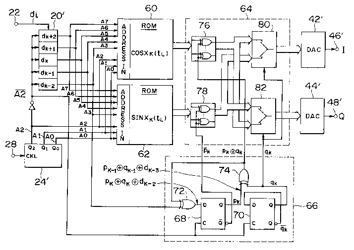
The arrangement shown ln Flg. 4 is based on theabove-mentloned prlnciple as expressed by equatlon (14), and
lncludes a shlft reglster 20', a counter 24', two ROMs 60 and
62, an output controller 64, a sequentlal loglc 66, and two
dlgltal-to-analog converters (DACs) 42', 44'. The blocks 20',
24', 42' and 44' are respectlvely ldentlcal wlth the blocks
20, 24, 42 and 44 ln Flg. 1 and hence wlll not be dlscussed ln
detall for brevlty. It should be noted that the Flg. 4
arrangement ls conflgured under the assumptlon of M=2 and N=8.
The ROMs 60 and 62 respectlvely pre-store the data
of cos Xk(tL) and sln Xk(tL).
The sequentlal loglc 66 comprlses two D-type fllp-
flops 68, 70 and two excluslve-OR gates 72, 74. As shown, the
shlfted lnput data dk 2 ls applled to one lnput terminal of
the exclusive-OR gate 72, whlle the clock slgnal /A2 ls
applled to a clock termlnal of each of the fllp-flops 66, 68.
The output of the excluslve-OR gate 72 ls deflned by
"Pk ~ qk ~ dk 2"' whlle one of the lnputs to the excluslve-OR
gate 74 ls deflned by Pk_l ~ qk-l k-3
The output controller 64 lncludes two output
polarlty controllers 76, 78 and two lnput data selectors 80,
82. The polarlty controller 76 ls supplled wlth the output of
the excluslve-OR gate 74 (vlz., Pk ~ qk) and reverses the
output of the ROM 60 ln the event that Pk ~ qk = 1. On the
other hand, the polarlty controller 78 reverses the output of
the ROM 62 ln response to the varlable of state /Pk whlch
- 12 -
71024-151
.,
-~ 2035293
assumes a loglc 1 (viz., ln the event that Pk = ) The
polarlty controller 76 lncludes a plurallty of excluslve-OR
gates arranged ln parallel, each of whlch ls supplled wlth the
output of the ROM 60 at one lnput termlnal thereof and each of
whlch ls supplled wlth the above-mentloned Pk ~ qk.
Slmllarly, the polarlty controller 78 lncludes a plurallty of
excluslve-OR gates arranged ln parallel, each of whlch ls
supplled wlth the output of the ROM 62 at one lnput terminal
thereof and each of which ls supplled wlth the varlable of
state /Pk. The number of the excluslve-OR gates of each of
the polarlty controllers 76, 78 ls equal to the output llnes
(elght for example) of the assoclated ROM.
The lnput data selectors 80, 82 respectlvely select
the outputs of the controllers 76, 78 ln the event that the
variable of state qk assumes a loglc 0. Otherwlse, the
selectors 80, 82 respectlvely select the outputs of the
controllers 78, 76.
It should be noted that each of the ROMs 60, 62 ls
provlded wlth elght address llnes lnstead of ten llnes as ln
the case of the prlor art referred to ln connectlon wlth the
Flg. 2. This means that the memory capacity can be reduced to
one-fourth as compared wlth the above-mentioned prlor art. By
way of example, ln the event that M=2, N=8 and the word length
ls 8-blt, the number of words requlred ls markedly reduced to
256 words from 1024 words ln the case of the above-mentloned
prlor art. Accordlngly, the number of blts requlred by each
of the ROMs 60, 62 ls
256 words x 8 blts/word x 2 - 4k blts.
71024-151
r
- 2035293
In the above descrlption, two separate ROMs 60 and
62 are provided. However, lt ls wlthin the scope of the
present lnventlon to prepare a slngle ROM whlch lncludes two
memory sectlons for respectively pre-storlng the data of
cos Xk(tL) and sln Xk(tL). Further, each of the ROMs 60 and
62 can be replaced wlth a random access memory (RAM), ln the
case of whlch the data (cos Xk(tL), sln Xk(tLl) should be
transferred to the assoclated RAM prlor to the operatlon.
Stlll further, the counter 24' ls not llmlted to a counter
whlch counts up to a multlple of two. The counter 24' may
take the form whlch counts up an approprlate natural number
(N), ln whlch case the shlft reglster 20' operates ln
synchronlsm of a clock slgnal whose frequency ls l/N. Flg. 5
is a tlmlng chart lllustratlng the tlmlng of the slgnals shown
in Flg. 4.
While the foregolng descrlbes only one embodlment
accordlng to the present lnventlon, the varlous alternatlves
and modlflcatlons posslble wlthout departlng from the scope of
the present lnventlon, whlch ls llmlted only by the appended
clalms, wlll be apparent to those skllled ln the art.
71024-151