Note : Les descriptions sont présentées dans la langue officielle dans laquelle elles ont été soumises.
-- Z035425
TITLE OF THE lNv~ ION
AN OVERDISCHARGE AND OVERVOLTAGE PROTECTION CIRCUIT FOR A
BATTERY IN A PORTABLE AND MOBILE COMMUNICATION SYSTEM
BACKGROUND OF THE lNv~r.lION
The present invention relates to an overdischarge and
overvoltage protection circuit for a battery in a portable,
mobile, and radio communication system, more particularly to an
overdischarge and overvoltage protection circuit which rings
alarming sounds and disconnects power supply for battery
(preferably Lead-Acid battery) protection when the battery
overdischarges, or automatically disconnects a power supply when
an overvoltage is supplied while using an exterior power supply.
In general, Ni-Cd and Lead-Acid batteries are used mostly
for a main power supply of a mobile communication system. By the
way, the Lead-Acid battery is more employed than the Ni-Cd
battery since the Lead-Acid battery is cheaper than the Ni-Cd
battery.
- 2 - ~ ~3S~2s
FIG. 1 is a diagram of a conventional circuit, which
consists voltage comparators (Al) and (A2) of a battery
protection (2) which detect a voltage-state and generate outputs
to a control unit(3) when a voltage of a Lead-Acid battery is
applied, and the control unit(3) which alarms and displays a
warning signal through a speaker (6) and a display unit (6)
respectively according to the detected voltage-state.
FIG. 2 is a diagram showing discharging characteristics of
the battery, and operational aspect will now be described with
reference to FIGS. 1 and 2. A voltage of the Lead-Acid battery
(1) is applied to non-inverting input terminals (+) of the
comparators (Al) and (A2). At this time, if the voltage of the
Lead-Acid battery is lower than a reference voltage, a signal
for a low-battery (hereinafter referred to as Low-Bat), which is
a logic low state of voltage of the battery, is generated by the
voltage comparator (Al) and applied to the control unit (3) in
order to generate a warning signal for recharge even though it
is possible to use as the present voltage. If a given voltage of
the Lead-Acid battery which is applied to non-inverting input
terminals (+) is lower than warning voltage, the voltage
comparator (A2) generates a warning signal for a battery
termination (hereinafter referred to a Bat-Term), that is a
logic low state which indicates the voltage of the Lead-Acid
battery (1) reached out of an usable limit, thus cutting off the
power supplying is necessary. This Bat-Term signal is applied to
the control unit (3). When the Low-Bat signal from the voltage
comparator (Al) is applied to the control unit (3), the control
3 ~3S425
unit (3) generates alarming sounds and a warning sign which
indicate a recharging is necessary since the voltage is low even
though it is still usable through the speaker (6) and the
display (5). However, if the Bat-Term signal from the voltage
comparator (A2) is applied to the control unit (3), the control
unit (3) generates alarming sounds and a warning sign, which
indicate that the voltage of the Lead-Acid battery (1) has
reached out of the usable limit and the main power supply has to
be turned off, through the speaker (6) and the display unit (5)
respectively. Also, in the mobile communication system, amounts
of power consumption from the Lead-Acid battery (1) at a stand-
by mode and a call mode are different. Especially, at the call
mode, a transmitter "Tx" which sends out a radio carrier
operates, thus more power is consumed than at the stand-by mode.
Lead-Acid battery (1) must be able to supply different amounts
of current for a warning level for Low-Bat and Bat-Term at the
stand-by mode and for a warning level for Low-Bat and Bat-Term
at the call mode according to the discharging characteristics
diagram as in FIG. 2. To perform the above-mentioned operation,
the control unit (3) shorts resistors "R3" and "R6" by switching
on switches "SWl" and "SW2" at the stand-by mode to increase
detection voltages of the voltage comparators (Al) and (A2). On
the other hand, at the call mode, by switching off the switches
"SWl" and "SW2", the detection voltages of the voltage
comparators (A1) and (A2) become different.
The conventional circuit as shown in FIG. 1 has a drawback
that there is no protection from overdischarge of the battery
- 4 - 2035425
when a malfunction occurs due to a shock by an exterior power
supply or a static electricity since it is not possible to
operate a switch to disconnect the main power supply in the
mobile communication system causing a short lifetime of a
battery. The other drawback is that there is no protection from
overvoltage when using an exterior power supply.
It is therefore an object of the present invention to
provide a circuit which protects a Lead-Acid battery from an
overdischarge state by alarming users by detecting an
overdischarge state of a Lead-Acid battery in two stages and by
disconnecting a power supply automatically when the power supply
is not disconnected.
It is another object of the present invention to provide a
circuit which protects a system from an overvoltage by
automatically disconnecting a power supply when the overvoltage
is supplied if an exterior power supply is used instead of an
internal battery.
BRIEF DESCRIPTION OF THE DRAWING8
For a better understanding of the invention and to show how
the same may be carried into effect, reference will now be
made, by way of example, to the accompanying diagrammatic
drawings, in which:
-- 5
20J54~
FIG. 1 is a conventional circuit;
FIG. 2 is a diagram showing discharging characteristics of
a battery;
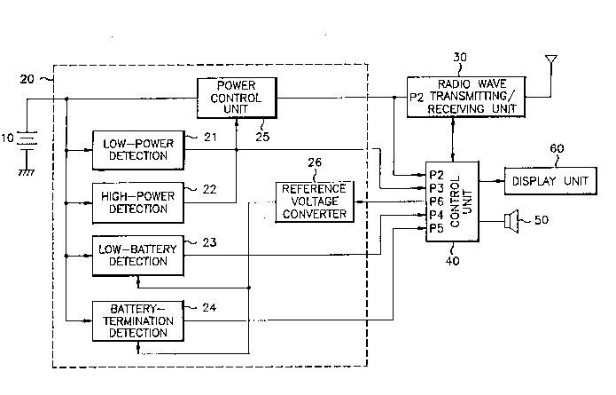
FIG. 3 is a system block diagram according to one embodimen~ of
the invention;
FIG. 4 is an embodiment of a circuit of an overdischarge and
overvoltage protection ~20); and
FIG. 5 is a flow diagram according to the embodiment of
FIG. 3.
DETAILED DE8CRIPTION
Referring to FIG. 3, a Lead-Acid battery (10) supplies a
power. A battery overdischarge and overvoltage protection (20)
generates an overdischarge warning signal according to a power
supply detection state when the Lead-Acid battery (10) is the
power source and cuts off power if an overvoltage state is
detected when using an exterior power supply. A control unit
(40) controls a system. A radio transmitting and receiving unit
(30) transmits and receives signals according to a controlling
signal from the control unit (40).
In the above-mentioned components, a formation of the
battery overdischarge and overvoltage protection unit (20) as
follows. A low-power detection unit (21) generates a control
signal for cutting off power when thç Lead-Acid battery (10) is
discharged to below a given reference voltage (9V). A high-
voltage detection unit (22) generates a controlling signal to
cutting off when an overvoltage above a given reference voltage
(17V) is detected when an exterior power supply is used. A low-
- 6 - 203S425
battery signal detection unit (23) generates a warning signal
for recharge when an voltage of Lead-Acid battery is below an
established reference warning voltage. A battery termination
detection unit (24) generates a signal to disconnect the power
supply when a voltage of the applied Lead-Acid battery is below
an established reference voltage of 9V. A power control unit
(25) disconnects the power supply according to controlling
signals from the low-power detection unit (21), the high-power
detection unit (22), the control unit (40). A reference voltage
converting unit (26) controls voltages through the low-battery
signal detection unit (23) and the battery termination detection
unit (24) by taking the controlling signal which distinguishes a
stand-by and a call modes from the control unit (40) as an
input.
Referring to FIG. 4, Between input terminals of a battery
power supply (P1) and a system power supply (P2), a MOSFET "Q1"
whose source and drain are connected by a diode (D1) is
connected, and a resistor "R22" is connected between a source
and a gate of the MOSFET "Q1". Between the gate of the MOSFET
"Q1" and a collector of a transistor "Q2", a resistor "R23" is
connected, and an emitter of the transistor "Q2" is grounded. A
resistor "R25" is connected between a base of the transistor
"Q2" and the ground, and a resistor "R24" is connected between
the base of the transistor "Q2" and a resistor "R25" which
connects to a 5V power supply. A resistor "R11" is connected
between the battery "P1" and a non-inverting input terminal (+)
of a first voltage comparator (All). A resistor "R12" is
~ 7 ~ Z03S425
connected between the ground and the non-inverting input
terminal (+) of the first voltage comparator (A11). To an
inverting input terminal (-) of the first voltage comparator
(A11), a reference voltage (5V) is applied. An output terminal
of the first voltage comparator (A11) is connected to a node
which connects to the resistor "R24" and the resistor "R26". A
resistor "R13" is connected between the input terminal of the
battery power supply "P1" and an inverting input terminal (-) of
a second voltage comparator (A12). A resistor "R14" is connected
between the ground and the inverting input terminal (-) of the
second voltage comparator (A12). To a non-inverting input (+)
terminal of the second voltage comparator (A12), a reference
voltage (5V) is applied. An output terminal of the second
voltage comparator (A12) is connected to the node which connects
to the resistor "R24" and the resistor "R26". The node which
connects to the resistor "R24" and the resistor "R26" is also
connected to a power control unit (P3) of the control unit (40).
A resistor "R15" is connected between the input terminal of the
battery power supply "P1" and an inverting input terminal (-) of
a third voltage comparator (A13). A resistor "R16" is connected
between the ground and the inverting input terminal (-) of the
third voltage comparator (A13), and an output from the third
voltage comparator (A13) is connected to an input terminal "P4"
of a low-battery signal. A resistor "R17" is connected between
the input terminal of the battery power supply "P1" and an
inverting input terminal (-) of a forth voltage comparator
(A14). Between the inverting terminal (-) of the forth voltage
comparator (A14) and the ground, a resistor "R18" is connected,
- 8 - ~ ~35425
and an output from the forth voltage comparator (A14) is
connected to an input terminal "P5" of a battery termination
signal. Between an input voltage "Vcc" of a power supply and the
ground, resistors "Rl9" through "R21" are connected in series,
and to a node which connects the resistors "Rl9" and "R20", non-
inverting input terminals (+) of the third and the forth voltage
comparators are connected. An input terminal of an inverter
(Il) is connected to an input terminal of a call/stand-by mode
control unit (P6), and an output terminal of the inverter (Il)
is connected to a node which connects to the resistors "R20" and
"R21". From the above stated components, a low-power detection
unit (21) which consists of the resistors "Rll" and "R12", and
the first voltage comparator (All) corresponds to the low-power
detection unit (21) in FIG. 3. A high-power detection unit (22)
which consists of the resistors "R13" and "R14" and the second
voltage comparator (A12) corresponds to the high-power detection
unit (22) in FIG. 3. A low-battery detection unit (23) which
consists of the resistors "R15" and "R16" and the third voltage
comparator (A13) corresponds to the low-battery detection (23)
in FIG. 3. A battery termination detection unit (24) which
consists of resistors "R17" and "R18" and the forth voltage
comparator (A14) corresponds to the battery termination
detection unit (24) in FIG. 3. A power control unit (25) which
consists of the resistors "R22" through "R26", the MOSFET "Q1",
and the transistor "Q2" corresponds to the power control unit
(25) in FIG. 3. A reference voltage converting unit (26) which
consists of the resistors "Rl9" through "R21" and the inverter
(Il) corresponds to the reference voltage converting unit (26)
- 9 - 203~;4Z5
in FIG. 3.
According to the above stated structure, an implementation
of the invention will be described with references to FIGS. 3
and 4. First, when the exterior power supply is used instead
of the Lead-Acid battery (10), due to a malfunction of the power
supply, if the overvoltage which is above the established
reference voltage (17V), is applied to the inverting terminal (-)
the second voltage comparator (A12) through the input terminal
of the battery power supply (P1), the second voltage comparator
(A12) generates a logic low signal as an output. Since the
second voltage comparator (A12) has an open collector
configuration, when the logic low signal from the second voltage
comparator (A12) is applied to the base of the transistor "Q2",
the transistor "Q2" turns itself off. When the transistor "Q2"
is off, a logic high signal is applied to the gate of the MOSFET
"Q1", and the MOSFET "Q1" turns itself off resulting in the
disconnection of the exterior power supply through the input
terminal of battery power supply (P1). At this time, a voltage
of power from the exterior power supply which is applied through
the input terminal of the battery power supply (P1) is divided
by the resistors "R13" and "R14". If the voltage divided by the
resistors "R13" and "R14" is called as VBH, then VBH = (R13 +
R14)*5V / R14. Here, the reference voltage is 17 Volts. When a
voltage higher than the reference voltage (17V) is applied to
the inverting terminal (-) of the second voltage comparator
(A12), the second voltage comparator (A12) recognizes above
station as the overvoltage, thus outputs a logic low signal.
- 2~35~25
However, when a voltage lower than the reference voltage is
applied to the inverting input terminal (-) of the second
voltage comparator (A12), the second voltage comparator outputs
a logic high signal. If a logic high signal is generated by the
second voltage comparator (A12), the power supply (5V) applies a
logic high signal to the base of the transistor "Q2" through the
pull-up resistor "R26" and the resistor "R24" causing the
resistor "Q2" to be on. If the transistor "Q2" turns on, the
exterior power supply which applies through the input terminal
of the battery power supply (Pl) flows through the resistors
"R22" and "R23". Because of this, a logic low signal is applied
to the gate of the MOSFET "Ql" turning the MOSFET "Ql" on. If
the MOSFET "Ql" is turned on, the exterior power which applies
through the input terminal of the battery power supply "Pl"
applies to input terminal "P2" of the system power supply.
On the other hand, when the Lead-Acid battery (10) is used
as a power supply, the power which applies through the input
terminal of the battery power supply "Pl" is applied to the non-
inverting input terminal (+) of the first voltage comparator
(All), and supplying power (5V) is applied to the inverting
input terminal (-) of the first voltage comparator (All). Here,
if the voltage which is divided by the resistors "Rll" and "R12"
is called as VBL, then VBL is (Rll+R12)*5Volts/R12. The
reference voltage is 9 Volts.
When a voltage lower than the reference voltage (9V) is
applied to the non-inverting input terminal (+) of the first
- 11 - 2Q35425
voltage comparator (A11), the first voltage comparator (A11)
estimates the voltage as a cut-off voltage, thus generates a
logic low signal. However, a voltage higher than the reference
voltage (9V) is applied to the non-inverting input terminal (+)
of the first voltage comparator (A11), the first voltage
comparator (A11) generates a logic high signal. When the first
voltage comparator (A11) generates a logic high signal, the
supplying power of (5V) applies to the base of the transistor
"Q2" through the resistors "R26" and "R24", therefore the
transistor "Q2" is turned on. When the transistor "Q2" turns on,
the exterior power supply which applies through the input
terminal (P1) of the battery power supply is applied through
the resistors "R22" and "R23". Also, a logic low signal is
applied to the gate of the MOSFET "Q1", turning on the MOSFET
"Q1". Here, a voltage between the source and the gate of the
MOSFET "Q1" is called as VGs, then VGs is -~R22/(R22+R23) * VB},
where VB is a voltage of the battery. When the MOSFET "Q1" turns
on, the power supplied by the Lead-Acid battery (10) applies to
the supplying power input terminal (P2) of the system, therefore
the power is applied to the radio transmitting and receiving
unit (30) and the control unit (40).
Referring to FIGs. 3 and 4, the reference voltage
converting unit (26) generates different reference voltages for
the stand-by mode and the call mode by taking a control signal
from the control unit (40) (as shown FIG. 3) which distinguishes
the call mode from the stand-by mode. During the call mode, a
logic high signal which is generated from the call/stand-by mode
- 12 - 2035425
control unit (P6) of the control unit (40) as shown FIG. 3, is
inverted to the logic low signal by the inverter (I1). Since the
inverter Il has an open drain configuration, when the output is
a logic low signal, the voltage VR generated through the line
"A" becomes {R20/(Rl9+R20))* 5 V. However, during the stand-by
mode, a logic low signal which is generated from the call/stand-
by mode control unit (P6) of the control unit (40), is inverted
to the logic high signal by the inverter (Il). Since the
inverter (Il) has an open drain configuration, when the output
is a logic high signal, the voltage VR generated through the
line "A" is {(R20+R21)/(Rl9+R20+R21)}* 5V. Therefore, the
reference voltages for warning from the low-battery detection
unit (23) and the battery termination detection unit (24) during
the call mode and the stand-by mode are different, and have four
different values as below.
VL-Bat(stby) = (R15+R16) * VR(stby)/R16
VL-Bat(call) = (R15+R16) * VR(call)/R16
VB-Trm(stby) = (R17+R18) * VR(stby)/R18
VB-Trm(call) = (R17+R18) * VR(call)/R18
where VL-Bat(stby) is the reference voltage for warning from the
low-battery detection unit (23) during the stand-by mode, VL-
Bat(call) is the reference voltage for warning from the low-
battery detection unit (23) during the call mode, VB-Trm(stby)
is the reference voltage for warning from the battery
termination detection unit (24) during the stand-by mode, and
VB-Trm(call) is the reference voltage for warning from the
- 13 - ~5425
battery termination detection unit (24) during the call mode.
However, since twelve volt Panasonic LCS2012APC Lead-Acid
battery is used in this embodiment, the reference voltages for
warning become as below.
VL-Bat(stby) = 11.5 V, VL-Bat(call) = 10.45 V,
VB-Trm(stby) = 10.65 V, and VB-Trm(call) = 9.7 V.
Therefore, a voltage divided by the resistors "R15" and
"R16" which applies through the input terminal (Pl) of the
battery power supply applies the inverting input terminal (-) of
the third voltage comparator (A13). Here, if the voltage which
applies the inverting input terminal (-) of the third voltage
comparator (A13) is lower than the reference voltage for warning
(11.5V for the stand-by mode and 10.45V for the call mode) which
applies the non-inverting input terminal(+) of the third voltage
comparator (A13), the third voltage comparator (A13) generates a
logic high signal. The logic high signal from the third voltage
comparator (A13) is applied to the input terminal (P4) of the
low battery signal in the control unit (40), and a warning sound
and a warning sign which indicate that a recharging of the Lead-
Acid battery (10) is necessary, are generated through the
speaker (50) and the display unit (60) by a software process
from the control unit (40). If the recharging of the Lead-Acid
battery (10) is not performed after the warning sound and the
warning sign from the speaker (50) and the display unit (60) are
generated, a voltage which applies through the input terminal
;~3S425
- 14 -
(P1) of the battery power supply is divided by the resistors
"R15" and "R16" and then is applied to the inverting input
terminal of the third voltage comparator (A13). Here, if the
voltage which generates the inverting input terminal (-) of the
forth voltage comparator (A14) is lower than the reference
voltage for warning (10.65V for the stand-by mode and 9.7V for
the call mode) which applies the non-inverting input terminal
(+) of the forth voltage comparator (A14), the forth voltage
comparator (A14) generates a logic high signal. The logic high
signal from the forth voltage comparator (A14) is applied to the
input terminal (P4) for the low-battery signal in the control
unit (40), and a warning sound and a warning sign which indicate
that a disconnection of the power supply from the Lead-Acid
battery (10) are generated through the speaker (50) and the
display unit (60) by a software process from the control unit
(40). If the power supply of the Lead-Acid battery (10) is not
turned off, even an established period (about 30 seconds) is
passed after the warning sound and the warning sign from the
speaker (50) and the display unit (60) are generated to notify
an user, then a logic low signal is generated through the power
supply control unit (P3) by the control unit (40). This turns
off the power supply control unit (P3) resulting in a
disconnection of the power supply of the Lead-Acid battery (10).
Referring to FIG. 5, the composition of the invention is as
follows. A first process determines the call mode or the stand-
by mode. A second process generates the warning sound and the
warning sign by detecting the low-battery warning signal which
- 15 - ~03S425
requires recharging of the battery after the call mode or the
stand-by mode is decided by the first process. A third process
generates a warning sound and a warning sign by detecting the
battery termination warning signal after the warning sound and
the warning sign are generated as in the second process. A forth
process turns the battery power off an establish time later by
resetting a timer after generating the warning sound and the
warning sign as in the third process.
According to the above-mentioned composition, an embodiment
of the present invention with a reference to FIG. 5. is as
follows. In a step 5A, the mode of the system is checked whether
the call mode or the stand-by mode. If the mode is the call
mode, in a step 5B, a call and stand-by mode control unit (P6)
of the control unit (40) generates a logic high signal, and if
the mode is the stand-by mode, in a step 5C a call/stand-by mode
control unit (P6) of the control unit (40) generates a logic low
signal. Also, in a step 5D, the low-battery signal is checked
whether the signal is a logic high signal or not. If the signal
is not a logic high signal, the step 5A is repeated, and if the
signal is a logic high signal, a step 5E is performed. In the
step 5E, the battery termination signal is checked whether the
signal is a logic high signal or not. If the signal is not a
logic high signal, a step 5F is performed, and if the signal is
a logic high signal, a step 5H is performed. In the step 5F,
the low-battery warning sign is indicated by the display unit
(60), and then a step SG is performed.
- 16 - 2~S425
In the step 5G, the warning sound is generated through the
speaker (50), and then the step 5A is repeated. In the step 5H,
the battery termination warning sign is indicated by the display
unit (60), and then a step 5I is performed. In the step 5I, the
warning sound is generated through the speaker (50), and in the
step 5J, the timer is reset, and then the step 5K is performed.
In the step 5K, the timer is checked whether the timer passes 30
seconds, and if the timer passes 30 seconds, a step 5L is
performed. In the step 5L, a logic low signal is sent to the
power supply control unit (P3) of the control unit (40) to turn
the power of the battery off.
As stated above, this invention is advantageous in such
ways as protecting the battery from an overdischarge state by
alarming users by detecting an overdischarge state of the
battery in two stages and by disconnecting a power supply
automatically when the power supply is not disconnected, and
protecting a system from an overvoltage by disconnecting a power
supply automatically when the overvoltage is supplied if an
exterior power supply is used instead of an inside battery.