Note : Les descriptions sont présentées dans la langue officielle dans laquelle elles ont été soumises.
GRADUATION CORRECTION APPARATUS 3 ~ ~ ~
The present invention relates to a gradation correcting
apparatus which is capable of correcting the gradation of
picture signals in picture apparatuses such as television
image receiving machines, video tape recorders and so on.
In recent years, the gradation correcting apparatus has
been regarded as important in terms of obtaining a more
dynamic expression of the picture signals on a cathode-ray
tube (CRT). This is especially so as television sets have
become larger in size, and higher in picture quality.
A conventional gradation correcting apparatus will be
described hereinafter in one example with reference to the
drawings.
Accordingly, an object of the present invention has been
developed with a view to substantially reducing the drawbacks
inherent in the prior art, and has for its object to provide
an improved gradation correcting apparatus.
Another object of the present invention is to provide an
improved gradation correcting apparatus, which detects that
portion of the picture having a particular color and
luminance. The histogram addition data in the generation of
the histogram is corrected so that the gradation of the
portion is enlarged.
In accomplishing these and other objects, according to
one preferred embodiment of the present invention, there is
provided an additional data summing controller and a color
correction detecting circuit, in addition to the conventional
construction. This new circuit is capable of controlling the
summing data for correcting the histogram in accordance with
the color component as well as in accordance with the
conventional luminance.
In accordance with the present invention there is
provided a gradation correcting apparatus comprising: a
histogram memory for obtaining a histogram of an input
luminance signal, wherein the histogram indicates how the
pixels per screen are distributed in accordance with the input
luminance signal; an arithmetic unit having the histogram data
outputted from said histogram memory as inputs, for
2 ~ Q ~
calculating a cumulative histogram and for normalizing the
cumulative histogram in accordance with a given luminance
level; an output circuit having the output of the arithmetic
unit as the input so as to synchronize said input luminance
signal with said normalized arithmetic unit output, outputting
output luminance data; a correction color detecting circuit
having at least one of an input color signal and the input
luminance signal as the input, for detecting a picture
component having at least either of a particular color and
luminance, and for outputting correction color detection data;
and a controlling circuit for correcting summing data in
accordance with the correction color detection data and for
adding the summing data to histogram memory output data to
obtain histogram memory input data to be stored in the
histogram memory.
The present invention will be described in detail
hereinbelow with the aid of the accompanying drawings, in
which:
Fig. 1 is a block diagram of a gradation correcting
apparatus in accordance with one embodiment of the present
invention;
Fig. 2 are graphs for illustrating the operation of
Fig. 1;
Fig. 3 is a block diagram of the conventional gradation
correcting apparatus; and
Fig. 4 are graphs for illustrating the operation of
Fig. 3.
Before the description of the present invention proceeds,
it is to be noted that like parts are designated by like
reference numerals throughout the accompanying drawings.
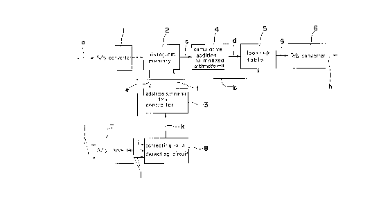
Fig. 3 is a block diagram of a conventional gradation
correcting apparatus. In Fig. 3, reference numeral 1 is an
analog to digital (AD) converter for converting an input
luminance signal, a, which is an analog signal into digital
data so as to output a luminance data signal, b. Reference
numeral 2 is a histogram memory. The histogram memory is a
memory where a memory address is set corresponding to the
B
luminance data signal, b. The address data is a histogram
which corresponds to the respective input luminance. The
luminance is read as histogram memory output data, e, in
accordance with the input luminance. In the histogram memory
2, after a particular summing data has been calculated into
the histogram memory output data, e, by an externally provided
adder 9, it is stored in an address corresponding to the
luminance of the input luminance signal (histogram memory
input data f). Here the particular summing data means, for
example, a "1".
Reference numeral 4 is a cumulative addition normalized
arithmetic unit, which cumulatively adds, as an input, the
histogram data, c, from the histogram memory 2. The output is
normalized to provide a maximum value of the output luminance.
This normalized signal is output as normalized histogram data,
d. Reference numeral 5 is a look up table which has memories
therein. The look up table 5 has addresses established in
accordance with the luminance of the luminance data b, and
stores the cumulative normalized histogram data, d, in the
address. The table then reads the data of the address
corresponding to the luminance data so as to be synchronized
with the input of the luminance data b, and outputs it as an
output luminance signal data, g. Reference numeral 6 is a
digital to analog converter (DA), which converts the output
luminance signal data, g, into an output luminance signal, h.
The operation of this gradation correcting apparatus will
now be described with reference to Fig. 3 and Fig. 4.
The input luminance signal, a, is converted into the
digital luminance data signal ,b, by the AD converter 1. The
data of the address of the histogram memory corresponding to
the luminance signal data, b, (luminance thereof) is selected
and becomes the histogram data memory output, e. Data, e, has
the addition data (1) added by the adder 9, and becomes
histogram memory input data, f, which is stored in the
previous address of the histogram memory 2. The histogram
contains or covers one or several frames of pictures in this
manner. The histogram obtained in this manner is shown in,
2~3~00
for example, Fig. 4 (a). After the histogram has been
provided, the data (histogram data c) from the histogram
memory 2 is read into the cumulative addition normalized
arithmetic unit 4 in order from the smaller address 5 (smaller
input luminance). The cumulative histogram is calculated in
the arithmetic unit 4, and the maximum value of the cumulative
value is normalized so that it becomes the maximum value of
the input luminance signal data. This is shown in Fig. 4 (b).
The normalized data is input into the look - up table 5 as the
cumulative normalized histogram data, d. The look - up table
5 is composed of a random access memory (RAM), where the
address is used as the input luminance and the data of the
address is used as the cumulative normalized histogram data,
d. When the data, d, is set into the look up - table 5, the
gradation correction is effected. In the gradation
correction, the input luminance signal data, b, is input into
the look - up table 5, an address is set in accordance with
the data, b, to read the data of the address. The data stored
at the address becomes an output luminance signal data, g,
(Fig. 4 (c)). The data, g, is input into the DA converter 6,
and is converted into an analog signal which is the gradation
corrected luminance signal, h. The above described processing
is generally called histogram conversion processing in the
field of the picture processing.
In such a conventional gradation correcting apparatus, no
problems are caused in the processing of white and black
signals. However, when this type of processing has been
applied to color picture signals, problems have arisen in that
the portion where the gradation which must to be actually
enlarged. That portion near the I shaft of the NTSC system
which is color sensitive are not sufficiently enlarged in
gradation. For example, the human face and eyes are not
sufficiently enlarged in gradation, because the color
information is not input.
The present invention will now be described.
5 ~Q~OO
In Fig. 1, a block diagram of a gradation correcting
apparatus according to one preferred embodiment of the present
invention is shown. The figure consists of an AD converter 1,
a histogram memory 2, a cumulative addition normalized
arithmetic unit, a look - up table 5, and a DA converter 6,
all of which are similar to those in the conventional
embodiment described in Fig. 3. Reference numeral 3 is a
summing data controller, which is adapted to add addition data
corresponding to color correction detecting data, k, into the
histogram memory output data, e, so as to output the histogram
memory input data, f. Reference numeral 7 refers to an AD
converter, which is adapted to effect the AD conversion of an
input color signal, i, (color carrier wave signal, color
difference signals R-Y, B-Y, G-Y or I, Q signals) so as to
output an input color data signal, j. Reference numeral 8
refers to a color correction detecting circuit, where the
input luminance data signal, b, and the input color data
signal, j, are provided as inputs, and a color portion for
strengthening the gradation correction is detected from the
size of these signals and output. The detected result is
color correction detection data, k.
The operation of the gradation correcting apparatus of
the present invention will now will be described with
reference to Fig. 1 and Fig. 2.
Fig. 2 shows the histogram conversion of the present
embodiment in the order of (a) (b) (c). The difference
between the conventional embodiment and the present embodiment
is the summing data controller 3, instead of the adder 9.
Summing data controller 3 is provided with the color
correction data signal, k, and histogram memory output data,
e. The color correction data signal, k is derived from the
luminance data signal, b, and the color data signal, j, which
is derived from the input color signal, i, via the AD
converter 7.
The input color signal data, j, and the input luminance
signal data, b, are input into the correcting color detecting
circuit 8 so as to detect a portion having the particular
color and luminance. In order to detect, for example, the
portion of the flesh tint, the computation of
a * (R - Y) - b * (B - Y )................. (1)
where the input color signal, i, shows the color difference
signals (R - Y) and (B - Y) where a, b are assumed to be
positive constants. When the result in the equation is large,
it is judged to be close to the flesh tint. As the flesh tint
is comparatively high in luminance, a judgment result that the
luminance is bright is added to the judgment result. Namely,
a portion where the size of the input luminance data signal,
b, input into the correction color detecting circuit 8 is
large is detected through the construction of a comparing
circuit and so on, so that the detecting result becomes
correct. In this manner, in the portion having the particular
color and luminance, the detection of the portion is effected
so as to output the correcting color data signal, k. This
signal, k, is input into the summing data controller 3. The
summing data controller 3 decides the summing data for adding
into the histogram memory data output, e, in accordance with
the correcting color data signal, k. Although, in the
conventional embodiment, a value 1 has been added, in the
present embodiment, the summing data is controlled so that it
may become larger when the particular portion has been
detected. Therefore, the summing data of the histogram memory
becomes larger in the portion detected by the color correction
detecting circuit 8. As a result, the cumulative normalized
histogram data, d, obtained through the cumulation and
normalization of the histogram obtained as described above
becomes larger in its inclination (variation amount) in the
portion detected by the color correcting detecting circuit 8
as described in Fig. 2 (b). As a result, the luminance in
that portion is enlarged as shown in Fig. 2 (c).
B
According to the present embodiment, a color signal AD
converter 7 for AD converting the color signal is provided. A
portion having a particular color is detected by the
corréction color detecting circuit 8 from the color signal
data, j, to be obtained by it and the input luminance data
signal, b, existing from the conventional embodiment. When
the summing data of the histogram memory 2 is added by the
results, the histogram summing data of the luminance portion
becomes larger by the provision of the summing data controller
3 for having the larger value, instead of the conventional 1,
as the addition data. As a result, the variation amount of
the luminance portion becomes larger when the cumulative
normalizing operation is effected, so that the gradation may
be enlarged.
Although the color difference signal have been used in
equation (1), the present invention can be implemented using
I, Q signals or the color carrier wave signal.
Although discrete circuits have been shown in the present
embodiment, it should be understood that a general purpose
arithmetic apparatus such as microprocessor or the like may be
used to implement the invention. Also, although the histogram
memory 2 and the look - up table 5 are shown separately, they
may use one memory in common.
B