Note : Les descriptions sont présentées dans la langue officielle dans laquelle elles ont été soumises.
RCA 85,411~~~~~~
- -1-
DIGITAL INTERPOLATION CIRCUITRY
This invention relates to circuitry for generating signal
values between known values as for example in expanding or
compressing video images.
In video signal expansion and compression systems it
is desired to perform a time scaling of discrete-time signals.
However, in order to realize a general scaling of the discrete-time
axis for the transformation y(m) = x(a~m), a major problem arises;
the input signal x(a ~ m) is undefined for non-integral values of its
index (a~m). Interpolation is the solution to this problem. When
the output requires a sample of the input at a time index with an
undefined input value, an interpolated value must be supplied. A
large body of literature exists on the topic of interpolation, but
several points are worth noting: a) interpolation which uses a
large number of input samples weighted with a sin(x)/x function
provides accurate results but is costly to implement for consumer
apparatus; b) sample-and-hold interpolation is the easiest to
implement but has generally poor performance; c) linear
interpolation is relatively easy to implement and provides
2 0 superior performance to the sample-and-hold technique, but
exhibits increasing attenuation with increasing signal frequency;
and d) higher order interpolation provides superior performance
to linear interpolation but exhibits nonlinearities.
T. J. Christopher in U.S. Patent No. 4,694,414 described
2 5 a relatively non-complex interpolator which exhibits relatively
accurate performance and which is realized with a parallel
combination of a two-point linear interpolator and a phase
compensation filter. The compensation filter has a transfer
function H(z) given by
3 0 H(z) _ -1 + z-1 + z-2 - z-3) ( 1 )
where z is the conventional "z" transform variable and the
exponents thereof correspond to the number of sample intervals.
It should be noted that the weighting coefficients are either plus
or minus one. The amplitude characteristic of the filter A(~) is
3 5 given by
A(~) = 2 cos (~/2) - 2 cos (3~/2)
where ~ represents frequency in radians per second.
RCA 85,411
-2-
The compensation filter is cascaded with a gain
element programmed with estimated gain values corresponding to
the possible positions at which the system is designed to produce
interpolated values. These gain values are derived by calculating
the response error at a particular signal frequency. Since these
gain values are not a function of frequency the response of the
Christopher system contains residual errors.
The present invention is directed to provision of a
relatively simple interpolation circuit, which has a substantially
accurate response characteristic for all signal frequencies up to
the Nyquist sampling limit of the system.
The present invention is a signal interpolator including
the parallel combination of a linear interpolator and a
compensating filter. The compensating filter is a finite impulse
response filter including tap weights, successive ones of which
follow a modified sin(x)/x function.
Brief Description of the Drawings
FIGURE 1 is a waveform diagram illustrating a sinc
sampling function.
2 0 FIGURE 2 is a graphical representation of a normalized
sinc function which may be utilized in an embodiment of the
invention.
FIGURE 3 is a block diagram of an interpolator system
embodying the invention.
2 5 FIGURE 4 is a block diagram of a compensating filter
which may be implemented for the filter 22 in FIGURE 3.
It is well known that ideal interpolation can be
achieved by convolving an input signal with a function S which
expresses the impulse response of an ideal low pass filter. For
3 0 continuous signals the function S is defined
S(t) = sin (2n(3t)/2n~it (3)
where ~i is equal to the Nyquist frequency and the function of
equation (3) is defined as the sinc function. The function S(t) is
illustrated in FIGURE 1. The discrete time interpolated value
3 5 corresponding to a particular time may be calculated from a
discrete time or sampled signal using the convolutions of S(t) and
the sampled signal g(Tn). That is, an interpolated sample value
g(to) for sample time to may be calculated from the sum of
RCA 85,411
-3-
products g(Tn) x Sn(to) where Sn(to) corresponds to a discrete
time version of the function S and is given by
Sn(t) = sin(2n(3(t-nT))/(2n(3(t-nT)) (4)
S More particularly, the interpolated value g(to) is given by
g(to) = E { g(Tn) x Sn(to) } (5 )
n=-
Note however that it is not practical to perform the computation
for all of the assigned values.
In order to implement the function in realizable
hardware the following constraints are used. 1) The number of
interpolated values between two sample points is limited to N
(e.g., N=64). 2) Only M samples preceding and M samples
following the point for which an interpolated value is to be
calculated are used in the calculation. In the embodiment shown
1 5 M is equal to four, thus a total of eight samples are used for each
calculation.
The sampling function Sn(t) is divided into a linear
part and a nonlinear part. More particularly the terms
S0(t) = F0(t) + (1-t/T) (6)
S 1 (t) = F1 (t) + t/T ( ~ )
and Sn(t) = Fn(t) for values of n except zero and
one.
2 5 The functions Fn(t) are further defined.
FO(t) = F1 (t) = k0 F(t) ( g )
F-1(t) = F2(t) = kl F(t) (9)
F-2(t) = F3 (t) = k2 F(t) ( 10)
F-3(t) = F4(t) = k3 F(t) ( 1 1 )
and
3 5 k0 = SO(T/2)-0.5 ( 12)
k1 = S1(T/2)-0.5 (13)
and the remaining kn are given by
RCA 85,411 '~ ~ ~~
-4-
kn = Sn(T/2) ( 14)
The function F(t) is defined
F(t) _ {S-1(t) + S2(t))/(2S2(T/2)~ (15)
where the argument t in equation 15 corresponds to the position
in time between the input sample points for which an interpolated
value is calculated and the terms S_1 and S2 in equation 15
conform to the sinc function as defined in equation 4. For
example, assume that the point for which an interpolated value is
to be calculated is between successive samples Sa and Sb and is a
1 0 distance (R/N)T from the first occurring sample Sa. The value
( 1-R/N)T is substituted for the argument t in equation 15 where
R/N(T) defines the fractional portion of the sample period T. The
values of F(t) for N equal to 64 are shown graphically in FIGURE 2.
Substituting equations 6-14 into equation S results in
1 5 g(to) _ (1-R/N)g(0) + R/N g(T) +
F(to)~{k3~g(-3T) + k2~g(-2T) + kl~g(-T)
+k0~g(0) + kl~g(T) + k2~g(2T) + k3~g(3T)
+k4~g(4T) } ( 16 )
The first two terms correspond to linear interpolation.
2 0 The latter terms correspond to a finite impulse response filter
function multiplied by the variable gain function F(t). The values
kn represent weighting coefficients applied to respective samples
g(nT). Table I illustrates the respective values of kn for an eight
tap filter.
2 5 TABLE I
k-3 = -2/(7n) _ -0.0909
k-2 = 2/(Sn) = 0.1273
k-1 = -2/(3n) _ -0.2122
k0 - 2/~- 0.5 = 0.1366
3 0 k 1 - 2/n-0.5 = 0.1366
k2 = -2/(3n) _ -0.2122
k3 = 2/(Sn) = 0.1273
k4 = -2/(7n) _ -0.0909
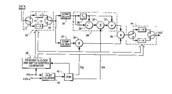
The interpolation system is shown in FIGURE 3. In this
3 5 embodiment it is in the environment of a video signal raster
mapper where for example compressed widescreen image
information is reformatted for widescreen image reproduction. It
is assumed that each horizontal line of video information consists
RCA 85,411 ~~~'~,~4~
-5-
of a sequence of compressed left side panel information, slightly
expanded center panel information, and compressed right side
panel information. The interpolator in this instance expands the
right and left sidepanel information and compresses the center
panel information to provide non-compressed/expanded lines of
horizontal information for utilization by a widescreen display
apparatus.
In FIGURE 3 the compressed/expanded video
information is applied to a data input terminal which is coupled to
1 0 a data buffer 10. The data buffer 10 includes a demultiplexing
switch 12, two one-horizontal line buffer memories 14 and 16 and
a multiplexing switch 18. The data buffer is controlled by a
control signal generator 38 to load incoming data in one buffer
memory while at the same time providing data (representing a
1 S previously stored line of information) from the second buffer
memory to the interpolator circuitry. The two buffer memories
alternate between receiving and outputing data. The receiving
memory is clocked at the rate of occurrence of incoming samples
while the outputing memory is clocked at a rate determined by
2 0 the interpolation function. The output clock rate may in fact be
the same as the input rate but operated in start/stop fashion.
A similar data buffer 44 is coupled at the output of the
interpolator to receive interpolated samples at one rate and to
provide interpolated samples at an output terminal OUT at a
2 5 constant rate.
The control of the entire system is provided by a
counter 40 and a read only memory 42, which provide control
signals to the clock control generator 38, the values F(t) to the
nonlinear portion of the interpolator and the values R/N to the
3 0 linear portion of the interpolator. At the beginning of each
horizontal line interval, the counter 40 is reset to a predetermined
value (e.g., zero), by a horizontal synchronization signal HORIZ.
Thereafter the counter 40 begins counting cycles of a clock signal
(4fsc) which is synchronous with the incoming data signal and has
3 5 a frequency at least as high as the incoming data rate. Each count
value provided by the counter corresponds to a known position on
the horizontal line of video information. The count values
provided by the counter 40 are coupled as address values to the
RCA 85,411 ' ~ r~ y, -;
_6-
ROM 42. The ROM is preprogrammed at its respective address
locations to provide the appropriate control signals to the
generator 38 and to provide the appropriate values corresponding
to F(t) and R/N.
The actual interpolator includes: a non-linear signal
path consisting of a compensation filter 22 and a multiplier 34; a
linear signal path including a compensating delay element 20 and
a linear interpolator 24; and a summing circuit 36 for adding the
signals processed in the two signal paths. Signal from the data
buffer 10 is coupled to both the linear and non-linear signal paths.
In the nonlinear signal path the signal is filtered in the
compensating filter 22 which is a finite impulse response filter
having symmetrical tap coefficients corresponding to the values
kn. Output signal from the filter 22 is coupled to the multiplier 34
1 5 wherein it is multiplied by the values F(t). Scaled values from the
multiplier 34, which conform to the non-linear portion of equation
16, are coupled to one input terminal of the summing circuit 36,
the output of which is coupled to the data buffer 44.
In the linear signal path, the input signal is coupled to
2 0 a delay element 20 which compensates for the difference in
processing delays between the linear and non-linear signal paths.
The output terminal of the delay element 20 is coupled to a one
sample delay element 26 and the minuend input terminal of a
subtracter 28. Delayed samples from the delay element 26 are
2 S coupled to the subtrahend input terminal of the subtracter 28.
Output differences from the subtracter are coupled to a multiplier
30 wherein they are multiplied by the value R/N. Respective
output samples from the multiplier 30 and the delay element 26
are coupled to first and second input terminals of an adder 32. If
3 0 the current sample provided by the delay element 20 is g( 1 ) then
the current sample provided by the delay element 26 is g(0). The
output signals provided by subtracter 28, multiplier 30 and adder
32 are (g( 1 )-g(0)); R/N(g( 1 )-g(0)); and R/N(g( 1 )-g(0)) + g(0)
respectively. The terms of the output signal from the adder 32
3 5 may be rearranged to R/N(g( 1 ) + g(0) ( 1-R/N) which conforms to
the linear response portion of equation 16. These sums are
coupled to a second input terminal of the s~imming circuit 36.
RCA 85,411 2 ~ '~ ~;
_7_
FIGURE 4 illustrates exemplary circuitry for realizing
the compensating filter 22. Since pairs of samples are weighted
with like coefficients, these pairs are first combined and then
weighted to reduce hardware. The particular filter shown is an
eight tap filter, however a filter of more or less taps may be used.
In FIGURE 4 input signal is applied to the cascade
connection of seven one-sample delay elements 52-64. Input
signal and delayed signal from delay element 64 are coupled to
respective input terminals of an adder 76. Output sums from
adder 76 are coupled to a multiplier 86 wherein they are
multiplied by the coefficient k4 to generate the sum of products
k4~g(4T) + k4~g(-3T) which is equal to k4~g(4T) + k_3~g(-3T) . The
sum of products provided by the multiplier 86 is coupled to an
adder 90 which provides the filter output signal corresponding to
1 5 the term in brackets in equation 16.
Delayed signals from delay elements 52 and 62 are
coupled to respective input terminals of an adder 74, the output
of which is applied to a multiplier 84. Sums of signals provided
by adder 74 are multiplied by the coefficient k3 in multiplier 84
to produce the sum of products k3~g(3T) + k3~g(-2T) which is
equal to k3 ~g(3T) + k_2~g(-2T). Output signals from multiplier 84
are coupled to the adder 90.
Delayed signals from delay elements 54 and 60 are
similarly coupled to an adder 72 and multiplier 82 combination
2 5 which provide the sums of products k2~g(2T) + k_ 1 ~g(T) to the
adder 90. Similarly, delayed signals from delay elements 56 and
58 are applied to an adder 70, multiplier 80 combination which
provide the sums of products kl ~g(T) + k0~g(0) to adder 90.
Adder 90 sums the output signals provided by the multipliers 80-
3 0 86 to produce the filter output signal.
It should readily be appreciated that the compensating
delay element 20 in FIGURE 3 may be eliminated by obtaining the
signal which is applied to the linear interpolator from the
appropriate delay element of the filter illustrated in FIGURE 4
3 5 (e.g., signal from delay element 56).
In addition the coefficients, kn, listed in Table I may
be modified slightly to facilitate hardware realization of the
multipliers by using the closet binary ratio to the coefficient. For
-8- ~U~~~~9 RCA85,411
example, kl, k2, k3 and lc4 may be 9, 14, 8 and 6 sixty fourths respectively,
or 17,
27, 17 and 12 one-twenty-Bights respectively. Similarly, the values of F(t)
may be
adjusted to equal a binary ratio. As such the multiplier may be realized with
shift-
and-add circuitry.
While the invention has been described in the environment of video
processing, it is to be understood that it is applicable to processing any
sampled
data signal.