Note : Les descriptions sont présentées dans la langue officielle dans laquelle elles ont été soumises.
11RC~4812
2U38~13
TRANSFORMER DIFFERENTIAL RELAY
Hackctround of the Invention
This invention relates to protective relay circuits for
use in AC power distribution systems and more particularly to
transformer differential relays.
As part of the protection scheme for AC power distribu-
tion systems, it is desirable to detect faults occurring within
the transformers used in the system. Upon detection of a fault
within the transformer, circuit breakers are operated to discon-
nect the input and/or the output of the transformer thereby pro-
tecting the transformer as well as those portions of the power
distribution system connected to the transformer.
Transformer differential relays have been used in the
past to detect faults within a transformer. Such relays operate
upon the theory that, in an unfaulted transformer, the current Ip
in the input windings is equal to the current Is in the output
windings multiplied by the output to input winding turns ra'io
Rt; that is, Ip = Rt Is. Upon occurrence of an internal fault,
the quantities Ip and Rt IS are no longer equal. Accordingly, a
transformer differential relay continuously compares the magni-
tude of the quantities Ip and Rt Is and will generate a trip
signal when the difference between the quantities Ip and Rt Is
exceeds a predetermined maximum. The trip signal is used to
operate one or more circuit breakers in order to disconnect the
11RC04812
2d3'~21'~
input and/or the output of the faulted transformer from the power
distribution system.
Although transformer differential relays work well to
detect the occurrence of internal faults, they have been known to
erroneously generate a trip signal as a result of transformer
inrush current. Transformer inrush current occurs as a result of
the application of voltage to the input windings. Voltage is
applied to the transformer input windings when, for example, the
system is initially powered or following the clearance of a fault
in the system. The presence of inrush current causes a differ-
ence to occur in the quantities Ip and Rt Is. When the differ-
ence exceeds the predetermined maximum, occasionally the relay
will generate a trip signal even thought the difference was
caused by inrush current and not by an internal fault. As a
result, the reliability of the relay and consequently the reli-
ability of the entire AC power distribution system incorporating
such a relay is diminished.
Therefore, it is an object of the present invention to
provide a method and apparatus for enhancing the reliability of
transformer differential relays.
It is another object of the present invention to pro-
vide a method and apparatus which enable transformer differential
relays to provide better discrimination between transformer
-2-
11RC04812
current differentials due to transformer inrush current and cur-
rent differentials due to the occurrence of a fault.
It is yet another object of the present invention to
provide a method and apparatus which enable transformer differen-
tial relays to prevent the occurrence of a trip signal based
solely on inrush current having a magnitude less than a predeter-
mined value.
It is still another object of the present invention to
provide a method and apparatus for generating additional trip
signal restraint in a transformer differential relay upon occur-
rence of an external fault.
It is a further object of the present invention to
provide a method and apparatus for increasing the reliability of
the transformer differential relay in the presence of current
transformer saturation on either internal or external faults.
It is yet a further object of the present invention to
provide a method and apparatus for generating an additional trip
signal operate quantity in a transformer differential relay when
transformer differential current exceeds a predetermined maximum
value.
These and other objects of the present invention will
become apparent to those skilled in the art upon consideration of
the following invention.
-3-
11RC04812
Summary of the Invention
The present invention comprises a transformer differen-
tial relay which includes means.for inhibiting generation of a
circuit breaker trip signal based solely upon transformer inrush
current having a magnitude which is less than a predetermined
maximum value. The trip signal inhibiting means comprises means
for generating a vector sum of signals related to currents in the
input and output windings of the transformer; means for measuring
the magnitude of the positive portions of the vector sum and the
negative portions of the vector sum; means for producing a re-
straint signal that is proportional to the absolute value of each
of the input and output signals related to the currents in the
input and output windings of the transformer; and means for pro-
viding a trip signal when the magnitude of the positive portions
of the vector sum exceed a first predetermined maximum value plus
the value of the restraint signal and the magnitude of the nega-
tive portions of the vector sum exceed a second predetermined
maximum value, plus the value of the restraint signal.
In the preferred embodiment, the vector sum of quanti-
ties relating to currents flowing in the windings of the trans-
former is generated as an operate signal. This vector sum operate
signal is applied to the input of a positive half wave rectifier
and the input of a negative half wave rectifier. The output of
the positive half wave rectifier is applied to an operate input
-4-
11RC04 ~~
of a summing and integrating amplifier. The output of the nega-
tive half wave rectifier is applied to the input of an inverter,
the output of which is applied to an operate input of a second
summing and integrating amplifier. The output of the first and
second summing and integrating amplifiers are applied to the
inputs of a first and second level detector respectively. The
first and second level detectors each generate an output signal
when the magnitude of the net input signal applied thereto ex-
ceeds a predetermined value.
The outputs of the first and second level detectors are
applied to the inputs of a two input and gate. Upon coincidence
of signals on the inputs of the and gate, an output trip signal
is generated. Consequently, a trip signal is generated when the
output of the first summing and integrating amplifier, Which is
related to the magnitude of the positive half wave rectified
vector sum operate signal less the restraint signal, exceeds the
predetermined threshold of the first level detector; and the out-
put of the second summing and integrating amplifier, which is
related to the magnitude of the negative half wave rectified
vector sum operate signal less the restraint signal, exceeds the
threshold of the second level detector.
Detailed Describtion of the Drawincts
While the specification includes claims particularly
pointing out and distinctly claiming that which is regarded as
-
11RC04812
2U38~1~
the present invention, the objects and advantages of this inven-
tion can be more readily ascertained from the following descrip-
tion of a preferred embodiment when read in conjunction with the
accompanying drawings in which:
FIGURE 1 is a schematic diagram of a step down trans-
former having a star connected side and a delta connected side.
FIGURE 2 is a schematic block diagram of a preferred
embodiment of an input portion of a transformer differential
relay in accordance with the present invention.
FIGURE 3 is a schematic block diagram of a preferred
embodiment of a harmonic restraint portion of the transformer
differential relay in accordance with the present invention.
FIGURE 4 is a schematic block diagram of a preferred
embodiment of the remaining portion of the transformer differen-
tial relay in accordance with the present invention.
FIGURE 5 is a schematic block diagram of a preferred
embodiment of a summing and integrating amplifier.
FIGURE 6 is a depiction of an exemplary waveform char-
acteristic of transformer inrush current.
Detailed Description of the Preferred Embodiment
The preferred embodiment of the transformer differen-
tial relay of the present invention is preferably used to protect
-6-
11RC04812
2U~8~~~
transformers which are utilized in three phase alternating cur-
rent electrical power distribution systems. The three phases are
typically referred to as phase A, phase B and phase C. The type
of transformers typically protected by transformer differential
relays include three phase step up and step down power trans-
formers. Such power transformers typically have a star connected
winding and a delta connected winding but may have two star con-
nected windings, a tapped star connected winding and a delta con-
nected winding (autotransformer), two delta connected windings,
or other combinations of star and delta connected windings.
Figure 1 schematically depicts an exemplary step down trans-
former, generally designated 10, which transforms a higher
voltage applied to its input windings, generally designated 12,
to a lower voltage produced at its output windings, generally
designated 14. It should be noted that the transformer depicted
in Figure 1 is merely exemplary for purposes of this detailed
description. Other types of transformers known by those skilled
in the art to be usable in electrical power distribution systems
are also protectable by the transformer differential relay of the
present invention.
As shown in Figure 1, the input windings 12 are con-
nected in a star configuration and the output windings 14 are
connected in a delta configuration as is known to those skilled
in the art. The input windings 12 are connected to phases A, B
and C of, for example, a high voltage transmission line; and the
11RC04812
~~~~~~.;~
output windings 14 are connected to phases A, B and C of, for
example, a low voltage distribution line. Current transformer
16, 18 and 20 are coupled to the phase A, B and C input windings
respectively; and each produces 'an output which is representative
of current flowing in the phase to which it is coupled. On the
output side, a current transformer 22 is coupled to the phase A
and phase H output windings: and produces and output signal which
is representative of the vector sum of the current -IA flowing in
the A phase output winding minus the current -IB flowing in the B
phase output winding. Similarly, current transformer 24 produces
an output signal which is representative of the vector sum of the
current -IB minus the current -IC flowing in the C phase output
winding; and current transformer 26 produces and output signal
which is representative of the vector sum of the current -IC
minus the current -IA. The use of such current transformers to
produce the signals indicated is well known to those of ordinary
skill in the art.
As pr wiously mentioned, transformer differential relays
operate on the principal that, in an unfaulted transformer, the
input current Ip is equal to the output current IS multiplied by
the output to input turns ratio Rt. In a three phase system, the
difference between the Ip and Rt Is quantities is usually mea-
sured for each phase current. For protected transformers having
delta connected windings, the individual phase currents IA, IB
_g_
11RC04812
and IC are beneficially resolvable into three vector sum currents
-IA +IB, -IB +IC and -IC +IA since such are relatively easy to
monitor using three current transformers coupled to the delta
windings as depicted in Figure l and described above.
Since it is necessary to monitor corresponding currents
on both the input and output sides of the protected transformer
in order that the difference between the Ip and Rt Is quantities
have the proper significance in determining transformer faults,
the_individual phase currents monitored by the current transformers
on the star connected side of the transformer will also be re-
solved into vector sum currents IA -IB, IB -IC and IC -IA as will
be subsequently described. In this regard, it should be noted
that the following detailed description is set forth with refer-
ence to one (IA -IB) of the three vector sum currents. Accord-
ingly, the preferred embodiment described herein is one of three
units, the other two units being associated with the IB -I~ and
I~ -IA vector sum currents in this example.
It has been foun.i in that transformer inrush current is
characterized by a substantially unipolar waveform which is es-
sentially a portion of a sinusoid. See, for example, the wave-
form depicted in Figure 6. This is to be contrasted with a fault
current which generally has a bipolar sinusoidal waveform. The
transformer differential relay of the present invention operates
on the principal that a circuit breaker trip output signal will
be generated upon sensing a current having a bipolar waveform,
-g-
11RC04~~~
the magnitude of which exceeds a first predetermined maximum
value; and inhibiting the generation of a circuit breaker trip
signal when the transformer current is substantially unipolar
with a magnitude less than a second predetermined maximum value.
Referring now to Figure 2, there is shown a schematic
block diagram of the preferred embodiment of an input portion of
a transformer differential relay in accordance with the present
invention. The input portion, generally designated 30, comprises
a first current transformer 32: a second current transformer 34;
and a third current transformer 36. In the preferred embodiment
described herein, these current transformers provide isolation
and internal phase shift. The most economical method of pro-
viding the ratio balancing taps should be determined in accor-
dance with the standard relay design practices as is known in the
art. Each current transformer has an input winding and an output
winding. A first resistor R1, is connected between a first ter-
urinal of the output winding of each current transformer and ref-
erence; and a second resistor R2 is connected between a second
terminal of the output winding and reverence such that the signal
present at the second terminal has an inverted polarity with re-
spect to the signal present at the first terminal.
The input winding of the first current transformer 32
is connected to a current transformer (not shown) coupled to the
phase A winding of the star connected side of the transformer
protected by the transformer differential relay. Accordingly,
-10-
11RC~
the signal present at the first terminal of the output winding of
the first current transformer 32 is related to the current IA
flowing in the phase A winding of the star connected side of the
protected transformer; and the signal present at the second ter-
urinal is a signal -IA having an inverted polarity with respect to
the signal IA. The input winding of the second current trans-
former 34 is connected to a current transformer (not shown) cou-
pled to the phase B winding of the star connected side of the
transformer. Consequently, the signal present at the first ter-
urinal of the output winding of the second current transformer 34
is related to the current IB flowing in the phase B winding of
the star connected side of the protected transformer; and the
signal present at the second terminal is related to -IB.
The signal IA from the first current transformer 32 is
coupled to one input of a first summing amplifier 38. The signal
-IB from the second current transformer 34 is coupled to a second
input of the first summing amplifier 38. Although the embodiment
described employs resistors connected between the tEr-minals of
the output windings and reference to obtain signals of inverted
polarity, a second winding on the current transformer (or a
tapped winding) could be beneficially employed instead. Alterna-
tively, an invertor might be used to obtain a signal of inverted
polarity although such might have a possible detrimental effect
of clipping on high currents.
-11-
11RC04812 ~
The input winding of the third current transformer 36
is connected to a current transformer (not shown) which is cou-
pled to the phase A and phase B windings of the delta connected
side of the protected transformer. The output of the current
transformer coupled to the phase A and phase B delta windings is
a signal related to the phase A current IA flowing in the phase A
delta winding minus the phase B current IB flowing in the phase B
delta winding. Accordingly, the output of the third current trans-
former 36 is related to the -IA +IB current flowing in the delta
connected side of the associated transformer. The output of the
third current transformer 36 is coupled to the input of a second
summing amplifier 42. The connection to the primary current
transformer (not shown) is such that on external fault currents,
or on load currents, the output of the summing amplifier 38 will
be equal (or almost equal) and approximately 180° out of phase
with the output of summing amplifier 42.
In those cases where the protected transformer includes
more than two windings, or in those cases where there is more
than one current transformer associated with each winding of the
protected transformer, it is preferred that additional signals
relating to the -IA +IB current be generated and coupled to the
input of additional summing amplifiers, a representative one
being shown as summing amplifier 44 in Figure 2.
The output of the summing amplifiers 38, 42 and 44 are
coupled to the inputs of a fourth summing amplifier 46. The
-12-
11RC04812
2~3~21~
output of the fourth summing amplifier 46 is a signal related to
the vector sum of the inputs and is utilized as a vector sum
operate (VSO) signal as will be subsequently described. The
outputs of the summing amplifier's 38, 42 and 44 are also coupled
to the inputs of absolute value circuits 48, 50 and 52 respec-
tively. Each of the absolute value circuits 48, 50 and 52 com-
prise a full wave rectifier. Accordingly, the output of each
absolute value circuit is a signal related to the full wave rec-
tified input signal. The outputs of the absolute value circuits
48,- 50 and 52 are coupled to the inputs of a fifth summing ampli-
fier 54.
The gain of the fifth summing amplifier 54 is selected
to have a magnitude of less than one such that the output signal
has a magnitude which is less than, or as will hereinafter be
referred to as a percentage of the total sum of the full wave
rectified outputs of the summing amplifiers 38, 42 and 44. The
output signal is utilized as a percentage restraint (PR) signal
as will be subsequently described. In the preferred embodiment,
the magnitude of the PR signal is, for example, 25% of the total
sum of the full wave rectified outputs of the summing amplifiers
38, 42 and 44. However, it should be noted that the percentage
could be less than or greater than 25% and could be adjustable,
for example over a range of from 15% to 40%. In addition, since
the present invention utilizes half-wave summing and integrating
amplifiers as will be subsequently described, the weighting of
-13-
11RC04812
2o~~z~~~
the percentage restraint will be a little more than one-half the
weighting that would be used on full wave summing and integrating
amplifiers.
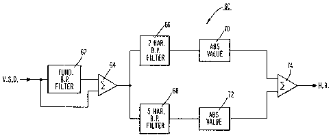
Referring now to Figure 3, there is shown a schematic
block diagram of a preferred embodiment of a harmonic restraint
portion of the transformer differential relay. The harmonic re-
straint portion, generally designated 60, comprises a first band
pass filter 62 having a Q on the order 1 to 2, a gain of minus 1
and a band pass center frequency tuned to the fundamental power
frequency, typically 60 Hz or 50 Hz. The vector sum operate
(VSO) signal from the fourth summing amplifier 46 of the input
portion 30 (previously described with respect to Figure 2) is
coupled to the input of the first band pass filter 62 and one
input of a sixth summing amplifier 64. The output of the first
band pass filter 62, which is the inverted fundamental frequency
of the VSO signal, is coupled to the other input of the sixth
summing amplifier 64. The sixth summing amplifier 64 sums the
algebraic values of the input signals; consequently, the output
of the sixth summing amplifier 64 is the VSO signal with the fun-
damental frequency removed. Accordingly, the output signal from
the sixth summing amplifier 64 includes the second and higher
order harmonics of the VSO signal.
The output of the sixth summing amplifier 64 is coupled
to the input of a second band pass filter 66 and the input of a
third band pass filter, 68. The second band pass filter 66 has a
-14-
11RC04812
Q approximately equal to 2: and a band pass center frequency
tuned to the second harmonic of the VSO signal. Consequently,
the output signal of the second band pass filter 66 is substan-
tially equal to the second harmonic of the VSO signal. This out-
put is coupled to the input of a fourth absolute value circuit
70. The third band pass filter 68 has a Q approximately equal to
2 and a band pass center frequency tuned to the fifth harmonic of
the VSO signal. Consequently, the output signal of the third
band pass filter 68 is substantially equal to the fifth harmonic
of VSO signal. This output is coupled to the input of a fifth
absolute value circuit 72.
The fourth 70 and fifth 72 absolute value circuits are
essentially full wave rectifiers whose output is substantially
equal to the full wave rectified input. The output of the fourth
absolute value circuit 70 is coupled to one input of a seventh
summing amplifier 74 and the output of the fifth absolute value
circuit 72 is coupled to the other input of the seventh summing
amplifier 74. The output of the seventh summing amplifier 74 is
a signal which comprises the algebraic sum of the input signals.
Consequently, the output of the seventh summing amplifier 74 com-
prises the algebraic sum of the full wave rectified values of the
second and fifth harmonic components of the VSO signal. The out-
put of the seventh summing amplifier 74 will be hereinafter re-
ferred to as the harmonic restraint (HR) signal.
-15-
11RC04812
20~~~~~
Referring now to Figure 4, there is shown a schematic
block diagram of a preferred embodiment of the remaining portion
of the transformer differential relay. The remaining portion,
generally designated 80, comprises a first level detector 82, a
first analog switch 84, a first summing and integrating amplifier
86 and a second summing and integrating amplifier 88. The first
86 and second 88 summing and integrating amplifiers each prefer-
ably comprises an operational amplifier 120 having a feed-back
circuit connected between its output and input as shown in Figure
5. The feedback circuit comprises a resistor 122 and a capacitor
124 connected in parallel. Each of the inputs to the summing and
integrating amplifier is connected to one side of a resistor 126.
The other side of each resistor 126 is connected to the input of
the operational amplifier 120 as depicted in Figure 5. The values
of the resistor 122 and capacitor 124 are selected such that the
summing and integrating amplifiers have a fairly long time con-
stant in order that the restraint built up in one half cycle does
not decay substantially to the next half cycle. A time constant
of approximately 1.5 cycles is preferred. The output of the opera-
tional amplifier 120 is the output of the summing and integrating
amplifier.
The summing and integrating amplifiers 86 and 88 are
utilized in the preferred embodiment of the present invention in
order to produce signals which are related to operate energy when
the magnitude of the sum of the operate signals applied to the
-16-
11RC0481~~~~~~~
operate inputs of the summing and integrating amplifier exceeds
the magnitude of the sum of the restraint signals applied to the
restraint inputs; and to produce signals which are related to
restraint energy when the magnitude of the sum of the restraint
signals applied to the restraint inputs exceeds the magnitude of
the sum of the operate signals applied to the operate inputs.
Although operate and restraint signals could be summed to produce
a net operate or restraint output signal, and such is considered
within the scope and contemplation of the present invention, it
is preferred to utilized operate and restraint energy, which is
the integration of the net operate or restraint output signal
over time, in order to eliminate erroneous, instantaneous re-
sponses.
The percentage restraint (PR) signal from the fifth
summing amplifier 54 of the input portion 30 (previously de-
scribed with respect to Figure 2) is coupled to the input of the
first level detector 82, the first analog switch 84, a negative
(or restraint) input of the first summing and integrating ampli-
fier 86 and a negative (or restraint) input of the second summing
and integrating amplifier 88. In this detailed description, the
terminology of a negative input implies a restraint signal into
the summing and integrating amplifier and a positive input im-
plies an operate signal. The magnitude of the sum of the re-
straint signals applied to the negative inputs must be exceeded
by the magnitude of the sum of the operate signals applied to the
-17-
11RC04~~~ ~ ~3 V
positive inputs of the summing and integrating amplifier in order
to generate a signal corresponding to net operate energy output
from the summing and integrating amplifier.
The first level detector 82 produces and output signal
when the input signal exceeds a predetermined maximum value. The
output of the first level detector 82 is coupled to the input of
a time delay circuit 90. The time delay circuit 90 produces an
output after the input signal has been applied for a predeter-
mined minimum period of time. In the preferred embodiment, this
predetermined period of time is approximately 110 degrees of the
360 degree period of the fundamental frequency; or, in the case
of a 60 Hz fundamental, the time delay circuit 90 will produce an
output after the input has remained applied for approximately 5.3
msec. The output of the time delay circuit 90 is applied to the
switch control input of the analog switch 84. Analog switch 84
couples the signal present at its input to its output upon re-
ceipt of a signal at its switch control input. The output of
analog s~Titch 84 is coupled to a restraint input of the first
summing and integrating amplifier 86 and a restraint input of the
second summing and integrating amplifier 88.
The output of the time delay circuit 90 is also coupled
to an inverted input of a first AND gate 92. The vector sum
operate (VSO) signal from the fourth summing amplifier 48 of the
input portion 30 (previously described with respect to Figure 2)
is coupled to the input of a first half wave rectifier 94 and a
_18_
11RC04812
203~2~3
second half wave rectifier 96. The output of the first half wave
rectifier 94 is the positive portion of the half wave rectified
input VSO signal. The output of the second half wave rectifier
96 is the negative por~ions of the half wave rectified input VSO
signal. The positive half cycles of the VSO signal are used as
an operate quantity of the first summing and integrating amplifier
86; and the negative half cycles of the VSO signal are used as an
operate quantity of the second summing and integrating amplifier
88 as will subsequently be described. The output of the half
wave rectifier 94 is coupled to the input of a comparator 98 and
a second analog switch 100 through a first diode 102. The output
of the first half wave rectifier 94 is also coupled to an operate
input of the first summing and integrating amplifier 86.
The output of the second half wave rectifier 96 is cou-
pled to the input of an inverter 104. The output of the inverter
104, which is the inverse of the negative portions of the half
wave rectified VSO signal coupled to the input, is coupled to the
input of the comp~~rator 98 and the second analog switch 100
through a second diode 106. The output of the inverter 104 is
also coupled to an operate input of the second summing and inte-
grating amplifier 88. A signal from an inrush set circuit 108,
which is representative of the maximum magnitude of transformer
inrush current expected for the protected transformer, is coupled
to the comparator input of the comparator 98. The inrush set
signal is also coupled to the other two phase units. The output
-19-
11RC04812
~~~~~~i
of the comparator 98, which occurs when the input exceeds the
signal level applied at the comparator input, is coupled to the
second input of the AND gate 92.
The output of the AND gate 92, which is produced when
there is a coincidence of a signal output from the comparator 98
and no signal output from the time delay circuit 90, is coupled
to the control signal input of the second analog switch 100. The
second analog switch 100 switches the signal at its input to its
output upon receipt of a signal at its control input. The output
of the second analog switch 100 is coupled to an operate input of
the first summing and integrating amplifier 86 and an operate
input of the second summing and integrating amplifier 88.
A bias voltage is coupled to a restraint input of the
first summing and integrating amplifier 86 and a restraint input
of the second summing and integrating amplifier 88. The magni-
tude of the bias voltage is selected to establish a minimum sen-
sitivity and to establish a restraint level in the summing and
integration stage in the qui,~scent state. The harmonic restraint
(HR) signal is coupled to a restraint input of the first summing
and integrating amplifier 86 and a restraint input of the second
summing and integrating amplifier 88. Although use of harmonic
restraint in the context of the present invention may not be nec-
essary, it is expected that CT saturation or transformer inrush
might require it. Consequently inclusion of harmonic restraint
-20-
11RC04812
203213
is preferred. The weighting of harmonic restraint will preferably
be established by test and may require field selection.
The output of the first summing and integrating ampli-
fier 86, which is a signal having a magnitude equal to the inte-
grated algebraic sum of the magnitudes of the input signals, is
coupled to the input of a second level detector 110. The output
of the second summing and integrating amplifier 88, which is a
signal having a magnitude which is substantially equal to the
integrated, algebraic sum of the magnitudes of the input signals,
is coupled to the input of a third level detector 112. The
second 110 and third 112 level detectors each produce an output
when the input signal exceeds a predetermined value. The output
of the second level detector 110 is coupled to one input of a
second AND gate 114. The output of the third level detector 112
is coupled to the other input of the second AND gate 114.
The output of the AND gate 114, which is produced
upon coincidence of a signal from th~ second level detector 110
and the third level detector 112, is hereinafter referred to as a
circuit breaker trip signal and is coupled to the circuit breakers
which are associated with the protected transformer. The second
110 and third 112 level detectors each preferably include a reset
timer with an estimated setting of approximately one cycle so as
to provide an overlap between the outputs when the inputs occur
-21-
11RC04812
during alternate half cycles; resulting in a nominal one cycle
operating time.
The transformer differential relay of the present in-
vention operates as follows. On external fault currents, or
heavy load currents, the transformer differential relay should
not operate. As previously stated, the connections to the relay
are such that, for example, on a two winding transformer, the
output of summing amplifiers 38 and 42 (see Figure 2) will be
approximately equal and 180 degrees out of phase. Thus, there
will be a percentage restraint signal into the summing and inte-
grating amplifiers 86 and 88 (see Figure 4); however, there will
be essentially no operate signal since the VSO signal will be
essentially zero.
Assuming that there is a fault current in the protected
transformer, the VSO signal will be a bipolar sinusoid as previous-
ly described. Consequently, there will be a positive output sig-
nal from the first half wave rectifier 94 and a positive output
signal from the inverter 104 which signals are applied to posi-
tive inputs of the first 86 and second 88 summing and integrating
amplifiers respectively. Accordingly, there will be an output
signal from both the first 86 and second 88 summing and integrating
amplifiers if the magnitude of the signals applied to the positive
inputs (operate signals) of the summing and integrating amplifiers
exceeds the magnitude of the signals applied to the negative in-
puts (restraint signals). Assuming that the magnitude of the
-22-
11RC04812
output signals from the first 86 and second 88 summing and inte-
grating amplifiers exceeds the levels set in the third 110 and
fourth 112 level detectors, the second AND gate 114 will produce
a circuit breaker trip signal. Thus, it can be seen that the
transformer differential relay of the present invention will pro-
duce a circuit breaker trip signal upon detection of an internal
fault current.
As previously stated, the transformer inrush current is
characterized by a signal having a waveform which is substantially
a portion of a sinusoid having a single polarity. Assuming the
presence of a transformer inrush current, the VSO signal, which
is representative of the vector sum of the currents IA -IB in the
transformer windings, will be in the form of a unipolar signal of
a portion of a sinusoid. Similarly, PR signal, which is related
to the vector sum of the absolute values of the IA -IB currents
in the transformer windings, will also be in the form of a
unipolar signal of a portion of a sinusoid. Assuming that the
half wave rectified VSO signal is unipolar in the positive direc-
tion an output will appear from the first half wave rectifier 94
which is applied to a positive input of the first summing and
integrating amplifier 86. However, no output will appear from
the second half wave rectifier 96 and consequently no output will
appear from the inverter 104 which is applied to the positive
input of the second summing and integrating amplifier 88.
-23-
11RC04812
Assuming the magnitude of the inrush current did not
exceed the maximum value set by the inrush current set circuit
108, there will be no output from the first AND gate 92. Conse-
quently, there will be no output from the second analog switch
100 which is applied to the positive inputs of the first 86 and
second 88 summing and integrating amplifiers. Since no positive
input signals have been applied to the second summing and inte-
grating amplifier 88, the output signal therefrom will not exceed
the predetermined level set in the third level detector 112.
Consequently, there will be no output from the third level detec-
for 112 and therefore no trip signal generated from the second
AND gate 114.
Assuming that the magnitude of the transformer internal
fault current is substantially larger than the expected maximum
value set by the inrush current set network 108, the comparator
98 will generate an output signal which is coupled to one input
of the first AND gate 92. The magnitude of PR signal will exceed
the level set in the first level detector 82. However, until tr.~
PR signal exceeds that level for more than 110 degrees, there
will be no output from the time delay circuit 90. Accordingly,
since there is no output initially from the time delay circuit 90
and there is a coincident output from the comparator 98, there
will be an output from the first AND gate 92 which will cause the
second analog switch 100 to couple the output signals from the
first half wave rectifier 94 (or the inverter 104) to positive
-24-
11RC04812
~03~~ I3
inputs of both the first 86 and second 88 summing and
integrating amplifiers. Such will cause the outputs of the
first 86 and second 88 summing and integrating amplifiers to
exceed the levels set in the second 110 and third 112 level
detectors respectively before time delay circuit 90
operates. Consequently, coincident outputs will appear at
the inputs of the second AND gate 114 causing the second AND
gate 114 to produce a trip signal. Thus, as can be seen
from the above description, the transformer differential
relay of the present invention will produce a very fast
output as a result of very large fault currents in the
protected transformer.
There is a possibility, albeit relatively remote, that
there will be an inrush to all three windings of a
transformer bank which will result in a dual polarity inrush
current in one of the three relays. For this reason, the
harmonic restraint utilized in prior art transformer
differential relays, has been retained in the relay of the
present invention. However, it is much lower in magnitude
than in prior art relays because dual polarity inrush
currents have a much higher percentage of harmonic currents.
See for example the paper entitled "A Dissertation on Power
Transformer Excitation and Inrush Characteristics", by J.
Berdy et al, presented to the Western Systems Coordinating
Council Relaying Committee, San Francisco, Calif . , Mar. 17,
1976.
-25-
,~;~.
11RC04~~~~~
In applications where one winding of the transformer is
connected to more than one set of current transformers, there is
a distinct possibility that one set of current transformers may
saturate on an external fault due to a difference in residual
flux level in the current transformers. The current transformer
with a residual flux in the same direction as that produced by
the first half cycle of fault current will most likely be the one
to saturate. To insure that the transformer differential relay
of the present invention does not produce a false trip output, a
variable restraint circuit is provided by level detector 82, time
delay circuit 90, and analog switch 84 (see Figure 4). In the
first part of the first half cycle of a fault current, before any
current transformer saturates, a restraint signal will build up
in the summing and integrating amplifiers 86 and 88 because the
percentage restraint signal (PR) will be large while the VSO
signal will be approximately zero. When one current transformer
saturates, the PR signal will be reduced and the VSO signal may
become substantially larger than the PR signal. However, before
the summing and integrating amplifiers 86 and 88 can reverse
their restraint energy, the time delay circuit 90 operates to
remove the additional operate signal via analog switch 100 and
increase the restraint signal via analog switch 84.
By contrast, on an internal fault the effect of current
transformer saturation is to permit a large relaying current in
the first part of the first half cycle of fault current; and,
-26-
11RC04812
2~13~~ ~.~
after the current transformer saturates, to substantially reduce
both the PR and VSO signals. Thus, on very large internal fault
currents, where current transformer saturation is probable, the
relay can operate in the first part of the first half cycle of
fault current, as previously described.
In view of the above, it can be seen that the present
invention enhances the reliability of transformer differential
relays by providing a method and apparatus for enabling the
transformer differential relays to discriminate between trans-
former current differentials due to transformer inrush current
and current differentials due to the occurrence of a fault.
While the present invention has been described with
reference to a specific embodiment thereof, it will be obvious to
those skilled in the art that various changes and modifications
may be made without departing from the invention in its broader
aspects. It is contemplated in the appended claims to cover all
variations and iuodifications of the invention that come within
the true spirit and scope of my invention.
-27-