Note : Les descriptions sont présentées dans la langue officielle dans laquelle elles ont été soumises.
203~3~
PHN 13.281 1 28.09.1990
Digltal recording and reproducing system.
The invention relates to a digital recording and
reproducing system, which system comprises a device for recording a
digital electric signal in a longitudinal track on a record carrier and
a device for reproducing the digital electric signal from the track on
the record carrier, which recording device has an input for receiving
the digital electric signal with a specific sample rate and is adapted
to convert the applied digital electric signal into a form in which it
can be accomodated in consecutive frames at a specific bit rate, which
frames can be recorded in the track on the record carrier, the
reproducing device being adapted to read the frames from the track on
the record carrier and being adapted to decode the information contained
in the frames into the digital electric signal having substantially said
sample rate and to supply said electric signal to an output, and the
invention also relates to a recording device and a reproducing device
for use in the digital recording and reproducing system, and to a record
carrier obtained by means of the recording and reproducing system in
accordance with the invention.
A recording and reproducing system of the type defined in
the opening paragraph is known, for example from the book ~The art of
digital audio~ by J. Watkinson, Focal Press 1988, Chapter 9. Chapter
9.20 of this book describes, for example, a system known as SDAT. In
this system a digital audio signal is recorded in a plurality of
juxtaposed tracks formed or to be formed on the record carrier in the
longitudinal direction of this record carrier. The recording device is
intended for recording a digital signal, such as a digital audio signal
originating from a digital signal source such as a Compact Disc audio
player, on the record carrier. For this purpose this digital signal
having a specific sample rate fs, which is fs = 44.1 kHz if the digital
~0 source is a CD player, is applied to the recording device. In the
recording device the digital electric signal is converted into a form in
which it can be recorded on the record carrier. Recording in the track
2~3.,~7~
PHN 13.281 2 28.09.1990
is effected at a bit rate which is neither equal to nor locked to the
salmple rate fs. For this purpose the recording device comprises a
se~parate frequency source ~crystal). However, now the problem may arise
that the sample rate at which the digital electric signal is applied to
the recording device varies. Moreover, the frequency supplied by the
frequency source may vary. The last-mentioned frequency variations may
be caused, for example, by temperature fluctuations affecting the
frequency source.
The recording device also has an analog input. An analog
electric signal applied Yl~ this input is sampled at a sample rate of
44.1 kHz and is digitized. In order to enable the analog signal to be
sampled at 44.1 kHz it is generally necessary to have a second frequency
source (crystal) to supply the sampling frequency of 44.1 kHz. However,
the frequency supplied by the second source may also vary. If the
digital signal is to be recorded correctly on the record carrier the
variations in the sample rate and the clock frequency of the first-
mentioned frequency source should be allowed for and should be
compensated for.
In the prior-art devices this is realised inter alia
by loading the samples of the digital signal, which are received with a
variable sample rate, into a memory and by reading them out of this
memory at a fixed frequency. Moreover, transport speed control is
applied to compensate for the variable bit rate with which the signal
processor in the recording device supplies the information in the frames
for recording on the record carrier.
It is an object of the invention to propose a digital
recording and reproducing system which in a different manner allows for
the variations in the sample rate with which the digital signal is
applied to the recording device and the bit rate with which the
information converted in the signal processor is applied to the write
head(s).
To this end the recording and reproducing system in
accordance with the invention is characterized in that the recording
device is adapted to record the frames alternately with interframe gaps
in the track on the record carrier, the reproducing device is adapted to
read the frames alternating with interframe gaps, and in that the
interframe gaps as recorded in the track on the record carrier have a
203~
P~N 13.281 3 28.09.1990
variable length. The recording and reproducing system may be
characterized further in that the frames as recorded in the track on the
record carrier have a variable length. The recording and reproducing
system may be characterized further in that the frames as recorded in
the track on the record carrier have a variable length.
The step underlying the invention is to refrain fIom
correcting for said variations at the recording side. This means that
the frames are recorded on the record carrier alternately with an
lnterframe gap having a specific nominal length. Variations in the
sample rate and the bit rate lead to variations in the length of the
interframe gaps, an increase (decrease) of the sample rate relative to a
nominal value of this sample rate (i.e. the 44.1 kHz) resulting in a
smaller (larger) interframe gap and in a smaller (greater) length for
the frame and a subsequent interframe gap. Moreover, an increase
(decrease) of the bit rate relative to a nominal value for the bit rate
leads to a larger (smaller) interframe gap, the overall length of a
frame and a subsequent interframe gap remaining the same.
The fact that no correction for bit rate variations is
applied during recording obviously does not mean that the recording
device does not require tape transport speed control. A control system
ensuring tape transport with a fixed nominal tape speed is always
needed. A correction for variations in the sample rate and the bit rate
at the recording side is now possible at the reproduction side by the
variations in the length of a frame and a subsequent interframe gap on
the one hand and by the variations in the length of the interframe gap
only on the other hand. At the reproduction side the digital electric
signal should, of course, be supplied with the sample rate of 44.1 kHz.
For this purpose the reproducing device comprises a frequency source
supplying a frequency which is related to the sample rate of the digital
electric signal appearing at the output of the reproducing device. This
frequency source may also supply a clock frequency which varies as a
result of inter alia temperature fluctuations to which the frequency
source is subject.
This means that in any case a compensation for said
frequency variations must be applied at the reproduction side. The
compensation means required for this purpose can then also be used to
compensate for the variations in the length of a frame and/or a
2 ~
PHN 13.281 4 28.09.1990
~subsequent) interframe gap of the signal read from the record carrier.
The interframe gap may comprise channel bits which
alternate with each bit cell. This means alternately ~zeros~ and
"ones". As already stated, the interframe gap should have a nominal
length to enable the length of this interframe gap to be increased or
reduced. Obviously, this nominal length depends on the nominal value of
the sample rate of the digital electric signal applied to the recording
device, on the nominal value of the bit rate with which the signal is
eventually recorded on the record carrier, and on percent variations
relative to these nominal values.
In the present example the nominal length of the
interframe gaps is selected to be 64 channel bits. In the case of a
maximum permissible variation of + 0.2% of the sample rate the
length of the interframe gaps then varies between 32 and 96 channel
1~ bits. If after conversion and insertion in the frames the digital signal
is recorded in a plurality of longitudinally juxtaposed tracks on the
record carrier, the frames will be recorded in the tracks in such a
manner that the interframe gaps of adjacent tracks are situated at
substantially the same positions, viewed in the longitudinal direction
of the record carrier and that adjacent interframe gaps have the same
length.
The recording device, comprising an input for receiving
the digital signal having the said sample rate, conversion means having
an input coupled to the input of the device, which means are adapted to
convert the digital electric signal into a form enabling it to be
accommodated in consecutive frames and to be supplied to an output at a
specific bit rate, which output is coupled to write means, for recording
the frames in the track on the record carrier, and a source for
supplying a clock signal of a certain clock frequency to an output,
which output is coupled to a clock signal input of the conversion means,
which clock frequency is in a fixed relationship to the bit rate at
which the signal is recorded in the record carrier, is characterized in
that the conversion means are adapted to generate alternately frames and
interframe gaps, which interframe gaps have a variable length related to
the variations in the sample rate and the clock frequency.
The reproducing device, comprising read means for reading
information from a track on the record carrier, decoding means for
~3~7~
PHN 13.281 5 28.09.1990
decoding the information accommodated in the frames into the digital
e:lectric signal having substantially said sample rate, which decoding
means have an input coupled to an output of the read means and have an
output for supplying the digital electric signal with a sample rate
substantially equal to said sample rate during recording, and a source
for supplying a clock signal of a specific clock frequency, which clock
frequency is related to the sample rate of the digital electric signal
supplied to the output, is characterized in that the device comprises
compensation means to compensate for the relative variations in the
length of a frame and a succeeding interframe gap in the signal recorded
on the record carrier and for the relative variation of the clock
frequency. In this way it is achieved that at the recording side no
correction is applied for the variations in the sample rate and the bit
rate, whilst at the reproduction side a correction is provided both for
the variations in the length of the frames and their succeeding
interframe gaps and the variations in the interframe gap itself and for
variations of the various clocX frequencies generated in the reproducing
device.
The reproducing device may be characterized further in
that the compensation means comprise a synchronizing-signal detector, a
phase comparator and tape-transport means, in that an input of the
synchronizing-signal detector is coupled to an output of the read means,
an output of the synchronizing-signal detector is coupled to a first
input of the phase comparator, an output of the clock-frequency source
is coupled to an input of the frequency converter, which has an output
coupled to a second input of the phase comparator, an output of the
phase comparator is coupled to a control input of the tape-transport
means, in that the phase comparator is adapted to generate a control
signal for the transport means to control the transport speed of the
record carrier in such a way that in the case of a deviation of the
clock frequency relative to the nominal clock frequency in a positive or
a negative sense the transport speed of the record carrier relative to a
nominal transport speed is varied in a positive sense and a negative
sense respectively, and in that in the case of a deviation of the length
of a frame and a succeeding interframe gap relative to a nominal length
of the frame and a succeeding interframe gap in a positive or a negative
sense the transport speed of the record carrier relative to the nominal
- ~3~7~
PHN 13.281 6 28.09.1990
transport speed is also varied in a positive sense and a negative sense
respectively.
Embodiments of the invention will now be described in
more detail, by way of example, with reference to the following
Figures. In the Figures
Fig. 1 shows an example of the recording device,
Fig. 2 illustrates the process of recording the
information on the record carrier depending upon variations in the
sample rate and the bit rate,
Fig. 3 shows the device of Fig. 1 in more detail,
Fig. 4 shows an example of a reproducing device,
Fig. 5 illustrates the process of reading the information
from the record carrier depending upon variations in ~he sample rate,
the bit rate and the length of the interframe gap,
Fig. 6 shows the reproducing device of Fig. 4 in more
detail, and
Fig. 7 shows some signal waveforms appearing in the
reproducing device shown in Fig. 6.
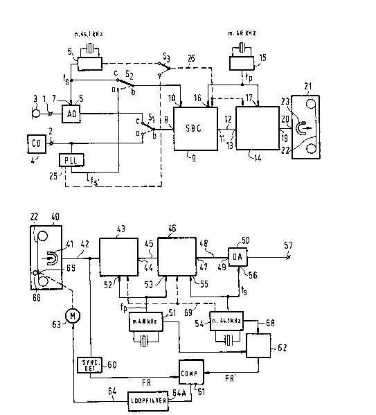
Fig. 1 shows diagrammatically an embodiment of the
recording device in accordance with the invention. The device comprises
an analog input 1 and a digital input 2. An analog audio signal, for
example generated by a microphone 3, can be applied to the device Y~a
the analog input 1. In the analog-to-digital converter 5 the analog
audio signal is sampled at a sample rate fs equal to 44.1 XHz, after
which the samples are digitized. For this purpose clock pulses of a
frequency equal to the sample rate fs are generated by the frequency
source 6, which comprises a crystal operating at a frequency which is a
multiple n of 44.1 kHz and which is applied to the clock signal input 7
of the A/D converter 5. In the present example n is 512. The crystal
then operates at a frequency of 22.579 MHz. The selector switch S1,
which is in position c-b, transfers the samples to an input 8 of a
coding unit 9, for example a subband coding unit S~C. Subband coding
units are described comprehensively in the literature, so that the
subband coding unit will not be described in further detail. The samples
from the A/D converter 5 are read into the subband coding unit 9 at a
~3~
P~N 13.281 7 28.09.1990
frequency corresponding to the sample rate fs. Therefore, the clock
pulses from the source 6 are applied to a clock pulse input 10 of the
coding unit 9 Yl~ the selector switch S2, which is in position c-b.
If a digital audio si~nal is applied to the input 2 the
S selector switches S1 and S2 are both in position a-b. ~y means of a
phase-locked loop 25 the sample rate fs~ is derived from the digital
signal. The digital signal is read in at this sample rate fs~ and is
transferred to the subband coding unit 9.
The subband coded signals are applied to the output 11
and are transferred to the input 13 of a digital signal processing unit
(or signal processor) 14 vra the line 12. The bit rate at which the
subband signals are applied to the signal processor 14 via the line 12
is, for example, 384 kbit/s. In order to realise this, clock pulses of a
frequency fp of m x 48 kHz are generated in a clock generator 15 and are
applied to clock pulse inputs 16 and 17 of the coder unit 9 and the
signal processor 14 respectively. A bit rate of 38q kbit/s cannot be
derived simply from the clock generator 6, which has a crystal operating
at 512 x 44.1 kHz. For this purpose the clock generator 15 is employed.
This generator 15 has a crystal operating at m x 48 kHz. In the present
example m is also 512, so that the clock frequency of the crystal is
24.576 MHz. The bit rate of 384 kbit/s can be derived simply from
frequency, namely by division by the number 64. In the signal processor
14 the signal i5 converted, for example, in an 8-to-10 con~erter. An 8
to 10 converter is described, for example, in the Applicant s European
25 Patent Application no. 150,082 (PHN 11.117). In this converter 8-bit
data words are converted into 10-bit code words. Furthermore, the signal
processor 14 can apply interleaving. All this serves to enable an error
correction to be applied to the received information at the receiving
side.
The error correction as applied in the system described
herein is described in the Applicant s prior European Patent Application
no. 90200128.8 (PHN 13.213).
As a result of this, the information stream (and hence
the bit rate) at the output 19 of the signal processor 14 is larger than
the information stream (bit rate) at the output 13. The information thus
obtained is accommodated in frames. 5ubsequently an interframe gap is
inserted between every two successive frames. The length of the
2~38~7~
P~N 13.281 8 28.09.1990
interframe gap will appear to be variable. In the present example the
nominal value for the interframe gap is taken to be 64 channel bits,
which value is subject to variations, as will become apparent
hereinafter. The signal thus obtained is supplied to the output 19. The
signal processor 14 converts the signal applied to the input 13 in such
a way that the bit rate at the output 19 is 768 kbit/s, i.e. twice the
bit rate at the input 13.
The output signal of the signal processor 14 is applied
to an input 20 of write means 21, by means of which the signal is
recorded in a longitudinal track on the record carrier 22. The write
means 22 may comprise one head or a plurality of heads, for example 8
juxtaposed heads, by means of which the information is recorded in 8
longitudinally juxtaposed tracks on the record carrier. In the last-
mentioned case a signal having a bit rate of 96 (= 768/8) kbit/s is
applied to each head.
A track now contains frames having a fixed information
content of 16320 bits, alternating with interframe gaps having a nominal
length of 64 channel bits. This means that one frame and a successive
interframe gap of nominal length situated in one track contain 16384
bits in total. This follows directly from the fact that in the present
example the frame period is 170~ ms. In the case of an in-track
bit rate of 96 kbitts it follows that a frame including an interframe
qap has a nominal length of 16384 bits.
The sample rates fs and fsl may vary. Similarly, the
frequency fp may vary. As a result of this there will be variations in
the length of the interframe gap (having a nominal length of 64 channel
bits) in the track, the length of the frame (which always contains 16320
channel bits) in the track, the bit rate at the output of the signal
processor 14 (having a nominal value of 768 kbit/s), and the frame rate
at the output of the signal processor 14 (having a nominal value of
375/64 = 96000/16384 frames/s).
When it is assumed that the maximum permissible variation
of the sample rate fs is 0.2% this means that the overall length of a
frame and a successive interframe gap in a track may exhibit a maximum
variation of 0.2% of 16384. This means a variation of 32 channel bits.
Consequently, the interframe gap, which contains a nominal numbeI of 69
channel bits, may have a length between 32 and 96 channel bits.
~3~7~
PHN 13.281 9 28.09.1990
The operation of the device will now be described in more
detail with reference to Fig. 2.
Fig. 2a illustrates a situation in which there are no
variations in the sample rate fs, i.e. fs is equal to the nominal
sample rate fsn, and in the clock frequency fp, i.e. fp is equal to
the nominal clock frequency fpn. On the upper line in Fig. 2a the
(nominal) program cycles in the microprocessor 19 are represented as a
function of time. The program cycles comprise program blocks Pn and
intervals T2. The upper line in Fig. 2b represents the data stream as
recorded in a track on the record carrier as a function of time, it
being assumed hereinafter that eight of these tracks extend parallel
adjacent one another on the record carrier. Since the record carrier is
moved at a constant speed this upper line also represents the physical
position of the data stream in the track on the record carrier.
The program blocks in the processor 14 have a length T1.
~etween two blocks a time interval T2 is interposed. In a program block
Pn the processor 14 prepares the data for recording: l~Ç~
interleaving, Reed-Solomon coding, and 8-10 modulation.
In a program block Pn the processor 14 processes the
information contained in 2048 information packets (slots) of 32 bits
each, which are supplied by the subband coder 9. As already stated, a
double amount of information is produced on the output, i.e. 2048 x 32
x 8 = 131072 bits. These bits are divided among 8 tracks and are stored
in these tracks. This means 16384 bits per track. However, the storage
of the actual information requires only 16320 bits per track, as already
stated above. This information is stored in one frame in the track. The
processor 14 interposes 14 interframe gaps In between the frames, which
interframe gaps have a nominal length of 64 (= 16384- 16320) channel
bits. At a bit rate of 96 kbitls this means that Tb is 0.66 ms. This
means that the connection between the output 19 of the processor 14 and
the input 20 of the write means 21 in fact comprises eight signal lines
for the transfer of the 8 signals to be recorded in the eight tracks.
The frames are recorded in the tracks in such a manner that adjacent
interframe gaps in the eight tracks all have the same length. The same
applies to the adjacent frames in the eight tracks.
Fig. 2b illustrates a situation in which the sample rate
fs deviates from the nominal value in such a manner that fs > fsn. This
- 2~3~
PHN 13.281 10 28.09.1990
means that the crystal in the generator 6 operates at a frequency higher
than n x 44.1 kHz. All the other parameters have not changed. Since fp
has not changed the processing time in the program block Pn remains the
same and is consequently equal to Tn. Similarly, the bit rate at which
the information is recorded in the track remains the same. This means
that the length of the frames Fn, viewed in time, is equal to the
nominal length Ta of the frames. Since fs > fsn the information stream
applied to the input 9 of the subband coder 9 i5 larger. Nevertheless,
the device should process this larger information stream. Eventually
this results in a larger information stream to be recorded in the
track. This is achieved in that the program cycles now succeed one
another more rapidly. The intervals T2' between the program blocks in
Eig. 2b are smaller than the intervals T2 in ~ig. 2a. Moreover, the
frames Fn succeed one another more rapidly, i.e. the frame rate has
increased. This is realised at the same bit rate by making the
interframe gaps smaller (I < In). Thus, the processor 14 inserts
interframe gaps of a length smaller than 64 channel bits in such a
manner that after processing exactly the increased information stream on
the input 8 can be recorded in the track on the record carrier. This
will be explained later with reference to Fig. 3. However, it is to be
noted here that variations in the crystal frequency n x 44.1 kHz of the
generator 6 affect the rate of information transfer between the coder
unit 9 and the processor 14 and, moreover, affect the starting instants
of the signal processing in the program blocks P in the processor 14.
This effect is represented diagrammatically by means of the broken line
26 in Fig. 1 and effect will be explained with reference to Fig. 3. The
variations of fs and fs~ are applied to the unit 6 and the processor
14 v a the switch S3, which should be in the appropriate position, and
the line 26.
Fig. 2c illustrates the situation in which the sample
rate fs is smaller than fsn, the other parameters again being the same.
Since fp is again equal to fpn, the program cycle Pn again has a length
of T1 and the bit rate at which the information is recorded in the track
is unchanged. This means that the length of the frames Fn is equal to
the nominal length Ta.
Since fs < fsn a smaller information stream is applied to
the input 8 of the subband coder 9. This also means that a smaller
~3nj ~7~
PHN 13.281 11 28.09.1990
information stream is to be recorded in the track. The program cycles
now succeed one another less rapidly. The intervals between the program
blocks of P are then larger, i.e. T2" > T2. Moreover, the frame
rate is reduced. This is achieved at the same bit rate by inserting
longer interframe gaps (I > In) between the frames. Thus, the processor
14 inserts interframe gaps of such a length that, after processing, the
information stream at the input 8 can be recorded exactly in the track.
Consequently, the interframe gaps become longer than 64 channel bits.
Fig. 2d illustrates a situation in which the clock
frequency fp is higher than the nominal clock frequency fpn. Again fs is
equal to fsn. The processor 14 now operates at a higher clock
frequency. The program blocks P are now shorter than T1. Moreover, the
bit rate at which the information is recorded in the track increases.
Since the information stream applied to the input 8
corresponds to the nominal information stream (fs is equal fsn) the
frame rate remains equal to the nominal frame rate of 375/64 frames/s.
Moreover, the overall cycle time in the processor 14, 1~
T1'+T2" ' remains equal to the nominal cycle time, i.e. T1tT2.
In the case of a higher bit rate of the information
stream on the record carrier an equal frame rate means that the physical
length of the frames in the track becomes smaller (F < Fn) and that the
length of the interframe gaps increases (I > In) in such a way that
Ta'+Tb' = Ta+Tb. The interframe gaps now contain more than 64
channel bits.
Fig. 2e illustrates the situation in which the clock
frequency fp is smaller than the nominal clock frequency fpn. In this
case fs is equal to fsn. The processor 14 now operates at a lower clock
frequency. The program blocks P are now longer than T1. Moreover, the
bit rate at which the information is recorded in the track decreases.
In the same way as in the situation illustrated in Fig.
2d the frame rate now also remains equal to 375/64 frames/s. The total
program cycle time, T" +T2"', is again equal to the nominal cycle
time T1+T2. This means that the intervals are smaller, T2'~ < T2.
In the case of a lower bit rate of the information stream
on the record carrier the equal frame rate results in an increased
physical length of the frames in the track F > Fn, and a reduced length
of the interframe gaps (I < In), in such a way that:
2 ~
P8N 13.281 12 28.09.1990
Ta "+Tb~ = Ta+Tb. From the above it also follows that the length of
the interframe gap as recorded in a track on the record carrier is
related to the ratio between fs and fp. If fs and fp both increase or
decrease, whilst their ratio remains the same, the length of the
interframe gap will not change. This can be demonstrated in qualitative
terms by comparison between Fig. 2b and Fig. 2d.
The operation of the device shown in Fig. 1, for
obtaining the output signals as illustrated in Fig. 2, will now be
explained with reference to Fig. 3.
Fig. 3 shows the frequency source 6, which comprises a
crystal 31 operating at a freguency of 512 x 44.1 kHz, i.e. 22.5792
MHz. In a divider 32, which forms part of the frequency source 6, this
frequency is divided by 512, yielding a frequency fs which is 44.1 kHz
in the nominal situation. It is obvious that in the case of the
frequency source 25, this source should comprise a PLL operating at a
~nominal) frequency of 512 x 44.1 kHz. For simplicity, however, the
second circuit shown in Fig. 1, including the switch S1, is not shown in
Fig. 3.
The 22.5792 MHz clock frequency is applied to a counter
33 ~}~ a frequency divider 32A, which divides the frequency of the
crystal 31 by four. The frequency source 15 in Fig. 1 comprises a
crystal 34 operating at a frequency of 512 x 48 kHz, i.e. 24.576 MHz.
This clock frequency is applied to a counter 35 yLa a frequency
divider 37, which divides the frequency of the crystal 34 by N. In the
nominal case N is 4, as will become apparent hereinafter. In a
comparator 36 the counts of the two counters 33 and 34 are compared with
each other in the following manner. The counters 33 and 35 are both 10-
bit counters. Counter 33 counts cyclically from 0 to 881 inclusive and
the counter 35 counts cyclically from 0 to 959 inclusive. ~oth counters
are started at the same instant and have a start value of zero. When the
counter 35 reaches the count ~69Y ~decimal) the count of the counter 33
is used for determining N in the divider 37. If this count is
substantially "0~ (decimal) N in the divider 37 is set to 4. If the
count of the counter 33 has not reached the value ~0~ at that time, N
will be taken equal to 6. If the count of the counter 33 is larger than
0, this results in N = 3. After this, the cycle is restarted, the value
for N obtained in a preceding cycle being stored in the divider 37, and
2~3~3~
PHN 13.281 13 28.09.1990
the counter 33 is not reset to zero but continues counting starting from
the value reached. In this way a phase-locked loop has been realized in
which fi is locked in phase to f5.
In this way the comparator 36 each time compares the
S count of the counter 33 with the value 882 and supplies a signal A to
define the value N in a manner as described above.
When both crystals 31 and 39 operate at their nominal
values N will be 4. A frequency f equal to 6.144 MHz then appears on the
output 39.
A variation of the clock frequency of the crystal 31 in a
positive sense (i.e. the crystal supplies a clock frequency higher
than 22.5792 MHz) means a higher count of the counter 33 and hence
another value of the control parameter A, i.e. such as to decrement
the value of N in the divider 37. The clock frequency fi supplied by
the divider 37 is then higher than 6.144 MHz. A variation of the clock
frequency of the crystal 31 in a negative sense then means that the
clock frequency supplied by the divider 37 is lower than 6.144 MHz. On
an average a variation in the clock frequency of the crystal 34 will not
result in a long-term variation in the clock frequency fi of the divider
37. Nevertheless, the clock frequency at the input 38 increases. For the
generation of the control parameter A an increase of the clock frequency
of the crystal 34 (while the frequency of the crystal 31 remains the
same) has the same effect as in the case that the clock frequency of the
crystal 31 decreases (while the frequency of the crystal 34 remains the
same). This means that the value N in the divider increases. Over a
longer period these two effects substantially cancel one another.
Therefore, it may be considered to derive fi only from the clock
frequency of the crystal 31. However, preferably this is not done
because deriving fi directly from the clock frequency of the crystal 31,
without allowing for the clock frequency of the crystal 34, requires the
use of inconvenient and difficult to realise dividing factors.
The nominal value of 6.144 MHz for fi can be derived
simply from the clock frequency of the crystal 34, namely by a division
~y four. Moreover, variations in the clock frequency of the crystal 34,
as explained hereinbefore, do not affect fi. In addition, the variations
in the clock frequency of the crystal 31 result in variations of fi, as
is desired.
2 ~ '3
PHN 13.281 14 28.09.1990
The clock signal from the divider 37 is applied to a
divider 71, which divides the clock frequency is by 512 so that a clock
signal of a nominal frequency of 12 kHz appears on the output. This 12
kHz frequency is applied to the subband coder 9' and to the processor
14. This frequency defines the data transfer between the subband coder
and the processor 14 and the data rate at which this transfer takes
place. This is because this 12 kHz frequency dictates the frequency at
which the information packets of 32 bits length are transferred to the
processor 14~ by the subband coder 9' YL~ the connection 12. This
results in a data transfer rate of 384 kbit/sec. For a further
explanation of the format of the signal applied to the line 12 by the
subband coder 9~ reference is made to the prior Netherlands Patent
Applications 89 01 401 ~PHN 12.967) and 90 00 338 ~PHN 13.241). This 12
kHz frequency is also applied to a divider 72, which divides the clock
frequency by 2048. This yields a nominal clock frequency of 375/64 at
the input 73. This clock frequency dictates and is equal to the frame
rate, and it is applied to the processor 14.
The 24.576 MHz clock frequency fro~ the crystal 34 is
also applied to the processor 14~ ~Ll a divider 74, which divides
the clock frequency by four. The processor now bears the reference
numeral 14~ to indicate that the unit 14~ represents that section of
the processor 14 which performs the signal processing upon the
information stream. Consequently, the processor 14 in Fig. 1 comprises
the section 14~ and some peripheral parts, such as some of the
counters and frequency dividers shown in Fig. 3. In fact the same
applies to the subband coder section which bears the reference numeral
9~ in Fig. 3.
The clock frequency of nominally 6.144 MHz from the
divider 74 is also applied to a divider 75, which divides the clock
frequency again by 128, so that a clock frequency of 48 kHz is generated
on the output. The output of this divider 75 is coupled to the c-
terminal of a switch S2. The output 76 of the processor 14~ is coupled
to the a-terminal of the switch 52. The processor 14~ further has an
output 77 on which a control signal is produced which is applied to the
control signal input of the switch S2. The b-terminal of the switch S2
is coupled to the output 19.
The device operates as follows. Again it is assumed that
2~3~37~
P~N 13.281 15 28.09.1990
all the parameters have their nominal values as illustrated in Fig. 2a.
The data is read in at 44.1 kHz, is processed in the subband coder 9
and is loaded into the signal processor 14~ at a bit rate of 384
kbit/s. This is effected under control of the 12 kHz clock frequency
from the divider 71. The clock frequency from the divider 72 dictates
the starting instants t1, t3, t5, see Fig. 2a, of the program blocks Pn,
in which the information applied to the signal processor 14 is
processed. The frequency fj from the frequency divider 74 dictates the
operating speed in the processor 14~ and thus determines the length
(t1, t2) of a program block. In a program block Pn a fixed amount of
information is processed in conformity with a fixed algorithm, so that
the frequency fj from the divider 74 dictates the length of the program
block. As soon as said fixed amount of information has been processed,
e. at the instant t2, which is ascertained internally in the
processor 14~, the processed information is output vla the output 76.
The processor 14' again ascertains internally when all the information
has been supplied to its output. This is at the instant t6, see Fig. 2a,
the lower line. In the time interval t2, t6 the switch S2 is position a-
b, so that the information from the processor 14~ can be applied to
the output 19. At the instant t6 the prscessor 14~ generates an IFG
control signal on the output 77, under the influence of which signal the
switch is set to position c-b. This IFG control signal remains available
on the output 77 until the processor 14' has internally ascertained
the termination of the next program block at the instant t4, so that the
IFG control signal disappears again. In the time interval t6, t4, in
which the switch S2 is consequently in position c-b, clock pulses having
a frequency of 48 kHz and supplied by the divider 75 are applied to the
output. In the nominal situation there are 64 clock pulses.
Consequently, the time interval t6, t4 has a nominal length of 0.66 ms.
At the instant t4 another program block is carried out. The amount of
information processed in this program block, during the time interval
t3, t4, is applied to the output 76 and is transferred to the recording
device 21 v a the switch S2, which is again in position a-b, in which
device said information is recorded on the record carrier in the time
interval Ta following t4.
Fig. 2b illustrates the situation in which fs is higher
than 44.1 kHz. This is because the frequency of the crystal 31 is higher
2~3~3~
PHN 13.281 16 28.09.1990
than 22.5792 MHz. This means that the information appears on the input 8
of the subband coder 9~ at a higher sampling frequency and is
consequently processed at a higher clock frequency, i.e. with a higher
speed, in this sùbband coder 9~. The frequency at the output of the
divider 71 is now higher than 12 kHz. This also means that the data
transfer rate to the processor 14 is now higher than 384 kbit/s. The
frequency generated by the divider 72 is also higher. This means that
the program blocks P succeed one another more rapidly. This can be seen
in Fig. 2b in that the time interval t1, t7 is smaller than the time
interval t1, t3 in Fig. 2a. Since the frequency fj, which is applied to
the input 17 of the processor 14~ and which dictates the speed of the
signal processing in the processor 14~, has not changed the processing
time in the processor 14~ has not changed. Viewed in time the length
of the program blocks has remained the same as in the situation
illustrated in Fig. 2a. The processor 14~ again internally detects the
instants t2, t8 at which the fixed amount of information has been
processed, so that it can be applied to the output. The switch S2 is in
position a-b, so that the information can be transferred to,the output
19. The processor 14~ further detects the instant t6 at which the
information is applied to the output 76. At this instant the IFG control
signal is applied internally to the output 77, so that the switch S2 is
set to position c-b and the 48 kHz clock pulses from the divider 75 can
be applied to the output 19 to produce the interframe gap. At the
instant t8 the processor 14~ detects the end of the next program
block. At this instant the IFG control signal is terminated, so that the
switch 52 is reset to position a-b. The information processed in the
next program block can then be applied to the output 19. The recording
time t2, t6 for the information in the record carrier is equal to the
recording time in Fig. 2a. Since the total time of a program cycle t2,
t8 is smaller than in Fig. 2a, the interframe gap is consequently
shorter.
The description of the operation of the circuit in the
situation illustrated in Fig. 2c can now be brief. If fs is smaller than
44.1 kHz the speed of information processing in the subband coder 9
and the speed of data transfer to the processor 14~ i5 lower.
Moreover, the frequency supplied to the processor 14~ by the divider
72 is lower. The clock pulses from this divider 72 dictate the
203~7~
PHN 13.281 17 28.09.1990
beginnings of the program blocks at the instants t1, t11, t13, see Fig.
2c. The time interval t1, t11 is now longer than the time interval t1,
t3 in Fig. 2a. However, for the remainder the signal processing in the
processor 14~ has not changed. This means that the switch S2 is in
position a-b during the time interval t2, t6 and in position c-b in the
time interval t6, t12.
Fig. 2d now illustrates the situation in which the clock
frequency fp from the crystal 34 is higher than 24.576 MHZ. AF stated
hereinbefore, these variations do not affect the clock frequencies
supplied by the dividers 71 and 72. However, the clock frequency
supplied by the frequency divider 74 changes. This clock frequency
increases. This means that the speed of signal processing in the
processor 14~ has increased. The length of the program blocks P has
consequently become shorter. In Fig. 2d this is visible in that the time
intervals t1g, t2 and t15, t4 are shorter than the time intervals t1, t2
in Fig. 2a. The pulses from the frequency divider 72 again dictate the
beginningc of the program blocks at the instants t14, t15, t16. The time
intervals t14, t15 and t15, t16 are equal to the time interval t1, t3.
This is because the crystal 31 again has its nominal frequency value and
the variation in the resonant frequency of the crystal 34 has no effect.
At the instant t2 the operation in program block P has
ceased and the information can be applied to the output 76 of the
processor 14'. Since fp is now larger than the nominal value fpn the
information is supplied more rapidly to the output 76 This means that
the information processed in a program block is recorded more rapidly
and hence in a shorter time interval t2, t17, on the record carrier. In
Fig. 2d this is visible in that the time interval t2, t17 is shorter
than the time interval t2, t6 in Fig. 2a.
At the instant t17 the processor 14~ again produces the
IFG control signal on the output 77, causing the switch S2 to change
over to position c-b. At this instant the clock pulses from the
frequency divider 75, which form the interframe gap, are recorded on the
record carrier. Since the frequency of the crystal 34 is higher than the
the nominal value of 24.576 MHz the frequency of the clock pulses
supplied by the divider 75 will be higher than 48 kHz. The bit rate of
the data supplied to the output 76 by the processor 14 and recorded on
the record carrier is now higher than the nominal bit rate of 96 kbit/s
2~3~37~
PHN 13.281 18 28.09.1990
per track.
Fig. 2e illustrates the situation in which the clock
frequency fp of the crystal 34 is lower than 24.576 MHz. Again this
variation has no effect on the clock frequencies supplied by the
S frequency dividers 71 and 72. However, the clock frequencies supplied by
the frequency dividers 74 and 75 change, i.e. decrease. This means that
the speed of signal processing in the processor 14~ is lower.
Consequently, the length of the program blocks P is greater than the
nominal length. In Fig. 2e this is visible in that the time intervals
t18, t2 and t19, t4 are longer than the time interval t1, t2 in Fig.
2a. The pulses from the frequency divider 72 again dictate the instants
t18, t19, t20 at which the program blocks P begin. The time intervals
t18, t19 and t19, t20 are equal to the time interval t1, t3.
At the instant t2 processing in the program block P is
completed and the information can be supplied to the output 76 of the
processor 19~. Since fp is now smaller than the nominal value fpn the
information is supplied more slowly to the output 76. This means that
the information processed in a program block is recorded more slowly,
i.e. in a longer time interval t2, t21, on the record carrier. In
20 Fig. 2e this is visible in that the time interval t2, t21 i5 shorter
than the time interval t2, t6 in Fig. 2a. At the instant t21 the
processor again produces the IFG control signal on the output 77, so
that the switch S2 is set to position c-b.
Since the frequency of the crystal 34 is lower than the
25 nominal value of 24.576 MHz the frequency of the clock pulses supplied
by the frequency divider 75 becomes smaller than 48 kHz. Moreover, the
bit rate of the data transferred to the output 76 by the processor 14~
and recorded on the record carrier is lower than the nominal bit rate of
96 kbit/s in a track.
Fig. 4 shows diagrammatically an embodiment of the
reproducing device in accordance with the invention. The device
comprises read means 40, comprising at least one read head 41, for
reading the information recorded by means of the device in Fig. 1 from a
track on the record carrier ~2. If the record carrier 22 again comprises
a plurality of tracks which are juxtaposed in the longitudinal direction
on this record carrier, for example 8 tracks, the read means will
comprise 8 read heads 41. The serial data stream read from the track
, 3 7 ~
PHN 13.281 19 28.09.1990
(tracks) is applied to a signal processing unit (or signal processor) 43
vla the line 42. In this signal processor 43 the information contained
in the frames is processed inversely to the manner in which the
information has been processed in the processor 1g shown in Fig. 1. This
means that deinterleaving and an error correction can be applied, and
that the 10-bit channel words are reconverted into 8-bit information
words in a 10-8 converter. This yields the subband signals, which are
applied from the output 44 to the decoder unit 46, in the present case
the subband decoder unit 46, via the line 45. In this subband decoder
unit 46 the subband signals are recombined to form a wide-band digital
signal. This wide-band digital signal is applied to the output 47 and,
YL~ the line 48, to the input 49 of the digital-to-analog converter
50. The device comprises a first frequency source 51, which supplies a
(nominal) clock frequency fp to a clock signal input 52 of the processor
43 and to a clock signal input 53 of the subband decoder unit 46. In
this case fp is equal to m x 48 kHz or 24.576 MHz. The clock frequency
at which the program in the processor 43 runs is derived from fp and the
~nominal) bit rate of 384 kb/s with which the information is applied to
the subband decoder unit 46 YL~ the line 45 is also derived from this
frequency fp.
The device further comprises a second frequency source
54, which generates a nominal sampling frequency fs and supplies it to a
clock signal input 55 of the subband decoder unit 46 and to a clock
signal input 56 of the D/A converter 50. Again this frequency fs is 44.1
kHz and is the frequency with which the samples are applied to the D/A
converter. For this purpose the frequency divider 54 again comprises a
crystal operating at a frequency of n x 44.1 kHz, where n is again 512,
so that the crystal operates at a frequency of 22.5792 MHz.
Subsequently, the analog signal appears on the output 57. The device
further comprises a speed control for the tape transport. This speed
control comprises a synchronizing-signal detector 60, a phase comparator
61, a frequency converter 62 and a control device for controlling the
transport speed of a motor 63 by means of a control signal which is
generated by the phase comparator 61 and is applied to the motor v'a a
loop filter 64A, comprising an integrator. This motor 63 drives a
capstan 64 which cooperates with a pressure roller 66 to provide the
transport of the record carrier 22.
2~3~37~
PHN 13.281 20 28.09.1990
~ y means of the sync detector 60 a f.eequency signal
related to the frame rate FR (in frames/s) in the signal being read is
derived from the signal read from the record carrier. The frame rate FR
can be derived from the serial oùtput signal supplied by the read means
40 in a manner as described with reference to Fig. 6. By means of the
frequency converter 62 a frequency FR' which is in a fixed
relationship to the desired frame rate is derived from the clock
frequency m.48 kHz from the frequency source 51. For deriving the
frequency FR~ the frequency converter 62 also receives the frequency
fs of n . 44.1 kHz from the frequency source 54, via the line 68. This
is necessary because variations of fs influence the value FR'. If fs
has exactly the nominal value of 44.1 kHz, F~' will be a multiple of
the nominal frame rate of 376/64. However, variations of the frequency
m.fp do not result in variations of FR'. In the comparator 61 the two
frequencies FR and FR' are compared with each other. From the
difference a control signal is derived for controlling the motor speed,
and hence the transport speed of the record carrier, Y~a the line 64.
The operation of the device shown in Fig. 4 will be described in more
detail with reference to Fig. 5.
Fig Sa is based on the no~inal situation. This means
that the sample rate fs is exactly equal to the nominal value fsn (=
44.1 kHz), the clock frequency fp is exactly equal to the nominal value
fpn ~= 24.576 MHz), the interframe gaps on the record carrier have
exactly their nominal length In (= 64 channel bits), and the frame rate
25 FR is exactly equal to the nominal frame rate FRN of 375/64 frames/s.
The tape transport is then effected at a speed Vt equal to the nominal
transport (or read) speed Vn. Fig. 5a therefore in fact corresponds to
Fig. 2a. The upper line represents the serial data stream of the frames
alternating with the interframe gaps in the time sequence in which they
are read. Since Vt = Vn this means that this line also represents the
physical position of the frames and the interframe gaps on the record
carrier.
The second line in Fig. 5a shows the program cycle
comprising program blocks Pn of a length T1 and intervals of a length
T2.
Fig. 5b represents the situation in which the sample rate
fs produced by the frequency source 54 is higher than the nominal sample
2~3~37~
P~N 13.281 21 28.09.1990
rate fsn, the other parameters being unchanged. Since fp has not changed
the processing time in the program block Pn remains the same and is
consequently T1. The higher sample rate for the samples applied to the
D/A converter 50 means that a larger data stream is applied to this D/A
converter 50. This also means that a larger data stream is to be read
from the record carrier 22.
Now a control signal is generated on the line 64 such
that the transport speed Vt increases (Vt > Vn). The frames Fn thus
recorded on the record carrier as illustrated in Fig. 5a are now read at
a faster rate. This is represented by means of the upper line in Fig.
5b. This line indicates how the information read from the record carrier
is applied to the signal processor 93, as a function of time.
As is apparent from Fig. 5b, the frames now succeed each
other more rapidly (Tal+Tbl < Ta+Tb). Similarly, the program blocks,
which basically have the same length as in Fig. 5a, now succeed one
another more rapidly viewed in time (T2' < T2). Consequently the
program cycle is shorter. Both the frame rate and the bit rate of the
signal read from the record carrier are higher than the nominal frame
rate and the nominal bit rate respectively. It is obvious that the
transport speed is increased exactly as much as is necessary to allow
for the increased data stream at the input of the D/A converter 50~.
Fig. 5c illustrates the situation in which fs is smaller
than the nominal sample rate fsn, the other parameters being unchanged.
In the same way as in Fig. 5b the processing time in the
program blocks Pn remains the same, i.e. T1.fp is equal to fpn. The
lower frequency at the input 49 of the D/A converter 50 means that the
data stream at this input 49 is smaller than the nominal data stream at
this point. This also requires a smaller data stream on the line 42.
Consequently, a control signal is generated on the line 69 such that the
transport speed Vt of the record carrier 22 is reduced (Vt < Vn). The
frames, which have been recorded on the record carrier 22 in a manner as
illustrated in Fig. Sa, are therefore read with a delay. This is
represented by the upper line in Fig. 5c. The frames now succeed each
other more slowly (Ta~'+Tb'~ ~ Ta+Tb). Similarly, the program blocks
Pn succeed one another more slowly (T2" > T2). ~oth the frame rate
and the bit rate in the signal read from the record carrier 22 are
therefore smaller than the nominal frame rate and the nominal bit rate
2Q~837~
PHN 13.281 22 28.09.1990
re!spectively.
Again the reduction of the transport speed of the record
carrier is exactly as much as is necessary to allow for the reduced data
stream at the input 49 of the D/A converter 50~.
Fig. Sd illustrates a situation in which only the clock
frequency fp deviates from the nominal value, i.e. fp > fpn.
Since fs is equal to fsn the transport speed Vt remains
equal to the nominal transport speed Vn. The information read from the
record carrier, see the upper line in Fig. 5d, is the same as in the
situation illustrated in Fig. 5a. Only the program blocks P are shorter
(T1~ < T1). However, the total program cycle does not change
(T1'+T2''' = T1+T2).
Fig. 5e illustrates the situation in which fp < fpn. Now
the program blocks P are longer: T1'~ > T1. Conversely, the intervals
are smaller, e. T2~ < T2. However, the total program cycle has
not changed: T1"+T2" " = T1+T2.
Fig. 5f illustrates a situation in which the interframe
gaps on the record carrier are larger than the nominal interframe gaps,
i.e. I > In. On the record carrier an interframe gap larger than the
nominal interframe gap can be obtained in two manners, namely in that
during recording fs < fsn, see Fig. 2c, or in that during recording fp >
fpn, see Fig. 2d.
Starting from the situation of Fig. 2c, in which the
frames have been recorded on the record carrier in such a way that the
overall length of a frame and an interframe gap on the record carrier is
greater than the nominal length, the motor control in the reproducing
device will be such that in this case the read time for one frame and
one interframe gap corresponds exactly to the nominal read time Ta+Tb.
This means that the transport speed is increased (vt > vn). Since the
frame length on the record carrier in Fig. 2c is equal to the nominal
frame length this means that during reproduction at a speed vt > vn the
read time Talll for a frame is smaller than the nominal read time Ta.
This means that the read time Tb~ for the interframe gaps during
reading is longer than the nominal read time for said interframe gap
Tb. This is illustrated in Fig. 5f.
Starting from the situation in Fig. 2d, in which the
frames and interframe gaps are arranged on the record carrier in such a
2~3~37~
PHN 13.281 23 28.09.1990
manner that the total length of a frame and an interframe gap i5 exactly
equal to the nominal length Ta+Tb, this means that during reproduction
the transport speed Vt of the record carrier is selected to be equal to
the nominal transport speed vn.
During reading the data stream therefore comprises frames
of a length smaller than the nominal frame length and an interframe gap
of a length greater than the nominal interframe gap length. This is
exactly as illustrated in Fig. 2d. The data stream being read, as
represented by the upper line in Fig. 5f, consequently also applies to
the reproduction of a signal recorded in a manner as illustrated in
Fig, 2d.
The program blocks have a duration equal to the nominal
program duration T1, because fp is equal to t,he nominal clock frequency
fpn.
Fig. 5g represents the situation in which a record
carrier is read with frames and interframe gaps such that the length of
the interframe gap on the record carrier is smaller than the nominal
interframe gap length. This is the situation as illustrated in Figs. 2b
and 2e. It is now assumed that the situation is as illustrated in Fig.
2b, where the total length of a frame and an interframe gap is smaller
than the nominal length. In the reproducing device the motor control
will control the motor transport in such a way that the total read time
for a frame and an interframe gap becomes equal to the nominal read time
Ta+Tb, see Fig. 5a, This means that the transport speed vt is smaller
than the nominal transport speed vn. Since the length of the frame in
Fig. 2b is equal to the nominal frame length, this means that the read
time for a frame is greater than the nominal read time Ta and the read
time for an interframe gap is smaller than the nominal read time Tb,
In the situation illustrated in Fig. 2e the total length
of a frame and an interframe gap on the record carrier is equal to the
nominal length. During reading the transport speed of the record carrier
will therefore be equal to the nominal transport speed. This means that
also in this case the read time for the frame is longer than the nominal
read time Ta and that the read time for an interframe gap is smaller
than the nominal read time Tb. In both cases a situation as illustrated
by the upper line in Fig. 5g is obtained. Since the clock frequency fp
is equal to the nominal clock frequency fpn the duration of the program
2&~33~ i~
~HN 13.281 24 28.09.1990
b:Locks is equal to the nominal program duration T1.
It is evident that variations of the crystal frequency,
n x 44.1 kHz of the generator 54 influence the speed of information
transfer between the processor 43 and the decoder unit 46 and also
influence the starting instants of the signal processing in the program
blocks in the processor 43, see Figs. 5b and c. This influence is
indicated diagrammatically by a broken line in Fig. 4 and will be
explained with reference to Fig. 6.
Fig. 6 shows the reproducing device of Fig. 4 in greater
detail, the operation of the device, as already illustrated by means of
Fig. 5, being described in more detail. The circuit shown in Fig. 6
comprises many parts also used in the circuit shown in Fig. 3. In Fig. 6
these parts bear the same reference numerals but primed.
The operation of the parts bearing primed reference
numerals is identical to the operation of the corresponding parts in
Fig. 3. This means that the frequency divider 71~ supplies a nominal
frequency of 12 kHz, which nominal frequency is not influenced by
variations of the frequency of the crystal 34~ but is affected by
variations of the frequency of the crystal 31~. Variations in the
frequency of the crystal 31~ in a positive sense (the value
increases) result in a higher frequency at the output of the divider
71~ and variations in a negative sense (the frequency of the crystal
31~ decreases) result in a lower frequency at the output of the
divider 71~. The frequency of this divider 71~ dictates the bit rate
of the information transfer between the processor 43~ and the subband
decoder unit 46~. In the nominal situation this bit rate is again
(12,000 x 32) = 384 kb/s.
The device further comprises a counter 80, a sampler 81
and the sync detector 60, as also shown in Fig. 4. The counter 80 and
the sampler 81 together constitute the phase comparator 61 in Fig. 4.
The counter 80 is an 8-bit counter which, under the
influence of the clock pulses supplied by the crystal 34~, counts from
0 to 255, after which it is restarted. At the instant at which a frame
starts, which instant is dictated by a clock pulse supplied by the
frequency divider 72~, the counter 80 is set to a specific starting
value, after which this counter proceeds to count under the influence of
the clock pulses from the crystal 34~. This is illustrated in Fig.
20~75
PHN 13.281 25 28.09.1990
7a. This Figure shows that the appearance of a pulse from the divider
72~, indicated by "strtfrm", causes the counter to be set to the count
~56~ ~decimal). The reason for this will become apparent hereinafter.
The sync detector 82 is adapted to derive the sync words
from the serial information stream being read. These sync words are the
block sync words in the signal. Each frame of the information signal as
recorded on the record carriér comprises a plurality of frame blocks.
Netherlands Patent Application no. 9001038 (PHN 13.314) states that a
frame in a track comprises 32 frame blocks. Each block comprises 51 10-
bit words. Consequently, a frame comprises 32 x 510 = 16.320 bits intotal. Each block comprises one block sync word. Consequently, the
detector 82 detects 82 block sync words in a frame. Fig. 7b shows the
output signal of the detector 82. It is evident that the detector 82
generates 8 pulses per frame at the output. In fact, this means that the
detector 82 detects every fourth block sync word, upon which it produces
a pulse on its output.
Each time that a pulse from the detector 82 appears on
its input 83 the sampler 81 takes over the count of the counter 80
applied to its input 84 and generates a control signal corresponding to
this count, which signal is applied, vla the line 64, to the motor 63
for driving the capstan 65. In the nominal situation, i.e. the
frequencies of the crystals 31~ and 34~ and the interframe gap
length on the record carrier all have their nominal value the pulses in
Fig. 7b are situated at such instants that the count is the stored in
the sampler 81 halfway the counts 0 and 255 (decimal), i.e. the count
127 or 128. The control signal on the line 64 is then such that the
motor control corrects the transport speed of the record carrier to be
exactly equal to the nominal speed vn, see Fig. 5a, so that the actual
frame rate FR corresponds exactly to the desired frame rate FR~, see
Fig. 4.
The instant at which a frame begins, which is the instant
of the first STRTFRM pulse in Fig. 7a, and the initial count to which
the counter 80 should then be set should of course be such that at a
clock frequency of 12 kHz, with which the counter 80 is driven after the
frequency division by 2048 in the divider 95, the counter has reached
the count 127 or 128 at the instant at which the first pulse appears on
the output of the block sync detector 82, i.e. the first pulse P1 in
2~3~7~
PHN 13.281 26 28.09.1990
Fig. 7b.
The pulses STRTFRM generated by the divider 72~ dictate
the instants t1, t2, t3, see Fig. Sa. If the information read from the
record carrier is adequate to enable the signal processing in the
S processor 43~ to be started, which is at the instant t4, this signal
processing is started until the entire operation in a program block is
completed. This is at the instant t2. At this instant the processor
43~ starts to accept information of a subsequent frame, so that
processing of this information can be started at the instant t5.
It is to be noted that in the present case the processor
bears the reference numeral 43~ and the decoder unit bears the
reference numeral 46~. The reason for this is that the unit 43~
forms that section of the processor 43 which performs the signal
processing upon the information stream. This means that the processor 43
in Fig. 4 comprises the section 43~ and some peripheral devices, such
as some of the counters and frequency dividers shown in Fig. 6. The same
applies to the subband decoder section 46~ in Fig. 6.
It is now assumed that the situation is obtained for
which fs ~ fsn. This means that the crystal 31~ operates at a higher
frequency than 22.5792 MHz, see Fig. 5b. As a result of this, the
frequency of the pulses on the output of the divider 72~ increases.
Therefore, the STRTFRM pulses succeed one another more rapidly. This
means that the counter 80 is sooner reset to the initial count and that
upon the next pulse, which is the pulse P1 in the signal shown in Fig.
7b, the count of the counter 80 is higher than 127 or 128. The sawtooth
curve shown in Fig. 7a has not changed because the counter 80 is driven
with a frequency derived from the crystal 34~ which still operates at
its nominal value. Thus, on the line 64 a control signal is generated
which causes the transport speed to increase until the pulses of Fig. 7b
appear at such instants that averaged over one frame the counts at the
instants of the pulses Pi in Fig. 7b, which are now spaced more closely
in time, are 127 or 128. This means that at the instants at which the
pulses P1, P2, P3, P4 appear the counts are larger than 127 or 128 and
at the instants at which the pulses P5, P6, P7 and P8 appear the counts
are smaller than 127 or 128. In more general terms this means that the
counts decrease each time at those instants at which the successive
pulses P1 to P8 appear within two consecutive STRTFRM pulses. Since the
2~3~7~
PHN 13.281 27 28.09.1990
motor control is an integrating control, see the loop filter 64A in
Fi.g. 4, the transport speed at said increased speed vt ~> vn) is
maintained and the count of the counter 80 remains 127 or 128 averaged
over a ~plurality of) frame~s).
Consequently, the frames as well as the interframe gaps
are read within a shorter time. This is illustrated by the upper line in
Fig. 5b. Since the processor 43 is opeIated at a nominal frequency of
6.144 MHz the signal processing performed in a program block takes the
same time as in the nominal situation.
Now it is assumed that the situation is obtained for
which fs < fsn see Fig. 5c. This means that the crystal 31~ operates
at a frequency below 22.5792 MHz. The frequency divider 72~ now
supplies the STRTFRM pulses at a frequency lower than the nominal
frequency of 375/64. This means that viewed in time the counter 80 is
reset to the initial count at a later instant and that upon the next
pulse, which is the pulse P1, in the signal shown in Fig. 7b the count
of the counter 80 is smaller than 127 or 128. Now a control signal is
generated on the line 64, which signal ensures that the transport speed
is reduced until the pulses shown in Fig. 7b, which are now spaced
further apart viewed in time, appear at such instants that considered
over one frame the counts still average 127 or 128. This means that at
the instants at which the pulses p1, p2, p3 and p4 appear the counts are
smaller than 127 or 128, whilst at the instants at which the pulses p5,
p6, p7 and p8 appear the counts are larger than 127 or 128. This is
because viewed in time the sawtooth curve shown in Fig. 7a has not
changed since the crystal 34~ operates at its nominal frequency. In
more general terms this means that the counts each time increase at
those instants of the successive pulses p1 to p8 which appear within two
consecutive STRTFRM pulses.
Since the motor control is an integrating control the
transport speed is maintained at the reduced speed vt (< vn) and,
averaged over a (plurality of) frame(s), the count is 127 or 128 at the
sampling instants represented by the instants at which the pulses from
the sync detector 82 appear.
Thus, the frames as well as the interframe gaps are read
from the record carrier over a longer time. This is illustrated by the
upper line in Fig. 5c. The time interval t1, t6 is shorter than the time
2~3~7~
PHN 13.281 28 28.09.1990
interval t1, t2. Since the processor 43 is operated at the nominal
frequency fpn of 6 144 MHz the signal processing performed in a program
block P takes as much time as in the nominal situation.
Now it is assumed that the situation is obtained in which
fp > fpn, see Fig. 5d. This means that the spacing between the STRTFRM
pulses has not changed. This is because variations of fp do not
influence the frequency supplied by the dividers 71' and 72'. On
account of the higher clock frequency applied to the counter 80 the
sawtooth shown in Fig. 7a, viewed in time, has a higher frequency.
Averaged over one frame the counts at the instants at which the pulses
p1 to p8 appear, will again be 127 or 128. This means that the counts at
the instants at which the pulses p1, p2, p3 and p4 appear are smaller
than 127 or 128 and the counts at the instants after the pulses p5, p6,
p7 or p8 are larger than 127. In more general terms this means that the
counts each time increase at those instants at which the successive
pulses P1 to P8 appear within two consecutive STRTFRM pulses. Averaged
over a (plurality of) frame(s) the count of the counter 80 remains 127
or 128. The transport speed of the record carrier then remains equal to
the nominal transport speed vn.
A similar line of reasoning applies to the situation for
which fp < fpn, see Fig. 5e. Viewed in time the sawtooth shown in Fig.
7a has now slowed down. This means that the counts at the instants at
which the pulses p1, p2, p3 and p4 appear are larger than 127 or 128 and
the counts at the instants at which the pulses p5, p6, p7 and p8 appear
25 are smaller than 127 or 128. In more general terms, the counts each time
decrease at those instants at which the successive pulses P1 to P8
appear within two consecutive STRTFRM pulses. However, averaged over a
(plurality of) frame(s) the counts are still 127 or 128 at a transport
speed equal to the nominal transport speed Vn.
In Fig. 5f the interframe gap on the record carrier is
larger than the nominal interframe gap. In the situation illustrated in
Fig. 2c the frames, including the interframe gap on the record carrier
then appear to be longer than the nominal length. Since the sawtooth
shown in Fig. 7a has not changed and the STRTFRM frequency has neither
changed the average count of the counter 80 in the case of a nominal
transport speed during reading would be too high for one frame period
(higher than 127 or 128). The transport speed is then increased so that
2~3~375
PHN 13.281 29 28.09.1990
averaged over a (plurality of~ frame(s) the count is again 127 or 128.
However, in a sitation as illustrated in Fig. 2d the counts during
reading at the nominal transport speed are already 127 or 128 averaged
over a (plurality of) frame~s). Thus, the nominal transport speed is
maintained Starting from both situations this means that a signal is
read as illustrated in Fig. 5f by the upper line. In Fig. 5g the
interframe gap length on the record carrier was smaller than the nominal
interframe gap length. If this concerns a situation as illustrated in
Fig. 2b the frames, including the interframe gaps, on the record carrier
appear to be shorter than the nominal length. Since the sawtooth shown
in Fig. 7a has not changed and the STRTFRM frequency has also remained
the same average count of the counter 80 at a nominal transport speed
during reading would be too low for a ~plurality of) frame~s).
Therefore, the transport speed decreases so that the average count again
15 becomes 127 or 128.
However, in the situation of Fig. 2e the counts during
reading at the nominal transport speed are already equal to 127 or 128
averaged over one frame period. Consequently, the nominal transport
speed is maintained.
It is to be noted that the invention is not limited to
the embodiments disclosed herein. Various modifications of the
embodiments described are possible without departing from the scope of
the invention as defined in the appended Claims.