Note : Les descriptions sont présentées dans la langue officielle dans laquelle elles ont été soumises.
- TITLE OF THE INVENTION 2 0 3 8~ 0 1
Method of Preparing Oxide Superconducting Thin Film
BACKGROUND OF THE INVENTION
The present invention relates to a method of preparing an oxide
5 superconducting thin film by a vapor phase method such as laser ablation,
for example.
BRIEF DESCRIPTION OF THE DRAWINGS
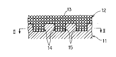
Fig. 1 is an enlarged sectional view showing a growth state of crystal
grains 13 in an oxide superconducting thin film 12 which is formed on a
10 substrate 11 according to the present invention in a model manner;
Fig. 2 is a sectional view taken along the line II - II in Fig. 1;
Fig. 3 is a sectional view illustrating a crystal lattice of an oxide
superconducting thin film 2 which is formed on a substrate 1;
Fig. 4 is a top plan view illustrating the crystal lattice of the oxide
15 superconducting thin film 2 shown in Fig. 3; and
Fig. 5 is a top plan view corresponding to Fig. 4, illustrating typical
examples of adjacent crystal lafflces whose a-axes and b-axes are
irregularized in an a-b plane.
In a typical example of a product which is prepared from an oxide
superconductive material, such as an oxide superconducting wire, for
example, an oxide superconducting thin film is formed on a suitable
substrate, so that the oxide superconductive material is held by the substrate
and shaped into a desired configuration.
- 1 -
, ~
203860 1
- In order to form such an oxide superconducting thin film on a
substrate as described above, a vapor phase method, for example, is
employed. Among various vapor phase methods, laser ablation has been
watched with interest particularly in recent years, due to its capability of
5 forming an oxide superconducting thin film under a low temperature at a
high speed.
Fig. 3 illustrates a crystal lattice of an oxide superconducting thin film
2, which is formed on a substrate 1 by a vapor phase method. As shown in
Fig. 3,
- la -
20~86~1
it is relatively easy to perpendicularly orient the c-axes
in the crystal lattice of the oxide superconducting thin
film 2 with respect to the substrate l. Such orientation
of the c-axes is easily attained particularly by laser
ablation.
On the other hand, Figs. 4 and 5 are top plan views
illustrating crystal lattices of the oxide superconducting
thin film 2 shown in Fig. 3.
As to such an oxide superconducting thin film 2, it
is known that current flows in a-b planes, which are
parallel to the surface of the substrate l. In order to
enable feeding of large current in the oxide
superconducting thin film 2, therefore, the directions of
the a-axes and the b-axes may be regulated as shown in
Fig. 4. In general, such a-axes and b-axes are
arbitrarily inclined as shown in Fig. 5.
In relation to such an oxide superconducting thin
film as shown in Fig. 5, it has been recognized that
critical current density Jc in a zero field as well as
critical current density Jc-B under a magnetic field are
reduced as inclination 3 between the a-axes of adjacent
crystal lattices is increased in a range of 0 to 45.
When the substrate l is formed of a polycrystalline
material, the directions of the a-axes and the b-axes are
easily irregularlized as compared with those of a single-
20~8601
crystalline substrate. In relation to this, it isnecessary to use a long substrate having proper
flexibility, in order to obtain an oxide superconducting
wire by forming an oxide superconducting thin film on such
a substrate. In general, it is difficult to provide a
long flexible substrate by a single-crystalline material.
In order to obtain a long flexible substrate, a
polycrystalline material must be employed in general.
SUMMARY OF THE INVENTION
Accordingly, an object of the present invention is to
provide a method of preparing an oxide superconducting
thin film, which can regulate directions of a-axes and b-
axes to the maximum on a polycrystalline substrate,
thereby attaining high critical current density.
The present invention is characterized in that, in a
method of preparinq an oxide superconducting thin fil~ by
forming such an oxide superconducting thin film on a
substrate through a vapor phase method, the substrate as
used is provided with a plurality of grooves in the same
direction on a surface to be formed with the oxide
superconducting thin film, in order to solve the
aforementioned technical problem.
When a long substrate is employed, the grooves are
preferably formed to extend along the longitudinal
direction of the substrate.
2038601
An average pitch between the plurality of grooves is
preferably selected to be not more than 10 ~m.
Preferably laser ablation is selected as the vapor
phase method.
While it is possible to form the grooves by scoring
the surface of the substrate with a knife edge, such
grooves are preferably formed by photolithography or beam
application, in particular.
When an oxide superconducting thin film is formed on
such a substrate according to the present invention, its
crystals are grown in parallel with the grooves, whereby
the directions of the a-axes and c-axes are regulated to
some extent.
Thus, according to the present invention, it is
possible to regulate the directions of the a-axes and b-
axes to some extent even if the substrate is formed of a
polycrystalline material, whereby current flowable in the
a-b planes can be increased. Therefore, it is possible to
obtain an oxide superconducting thin film, which exhibits
high critical current density Jc in a zero field as well as
high critical current density Jc-B under a magnetic field.
When a long substrate is employed and the grooves are
formed to extend along the longitudinal direction of such
a substrate, it is possible to obtain an oxide
superconducting wire having excellent superconductive
- 203~601
properties, which comprises an oxide superconducting thin
film formed on the long substrate.
It is preferable to densely form the grooves in the
narrowest possible width. Therefore, an average pitch
between the plurality of grooves is preferably selected to
be not more than 10 ~m.
The vapor phase method employed for forming the oxide
superconducting thin film is preferably carried out by
laser ablation. According to such laser ablation, not
only orientation of the c-axes is easily attained but the
film can be formed at a higher speed. Therefore, when an
oxide superconducting thin film must be continuously
formed on a long substrate in order to obtain an oxide
superconducting wire, for example, it is possible to
advantageously form the oxide superconducting thin film in
an efficient manner.
When the grooves are formed by photolithography or
beam application, it is possible to define sharp internal
angles at the bottom parts of the grooves. Such sharp
internal angles promote regulation of the directions of
the a-axes and the b-axes in crystal growth of the oxide
superconducting thin film.
These and other objects, features, aspects and
advantages of the present invention~will become more
apparent from the following detailed description of the
203860 1
present invention when taken in conjunction with the accompanying
drawings.
DESCRIPTION OF THE PREFERRED EMBODIMENTS
Examples of oxide superconducting thin films, which were prepared
5 by laser ablation according to an embodiment of the present invention, are
now described.
Experimental Example 1
An oxide superconducting thin film of YlBa2Cu307 ,~ was formed by
laser ablation on a substrate of YSZ (yttria
,~
203860~
-
stabilized zirconia; Y: 6 %) of 0.1 ~m in particle size.
The film forming conditions were as follows:
Laser: KrF (248 nm)
Energy Density: 2.3 J/cm2
Repetition Rate: 5 Hz
Oxygen Pressure: 300 mTorr
Substrate Temperature: 750C
Target-to-Substrate Distance: 45 mm
Film Forming Rate: 33 A/min.
Angle of Incidence of Laser Beam: 45
The film was formed under the above conditions for 4
hours. The as-formed oxide superconducting thin film
exhibited critical current density of 3400 A/cm2 in a zero
magnetic field.
On the other hand, grooves of 10 to 100 ~m in width
and 10 to 100 ~m in depth were provided on a similar
substrate in a groove-to-groove average pitch of 100 ~m
with a diamond cutter, and an oxide superconducting thin
film was formed on this substrate under the same film
forming conditions. This film exhibited critical current
density of 15000 A/cm2 in a zero magnetic field.
Experimental Example 2
Grooves of various sizes and directions were formed
on long substrates by photolithography or beam
application. Then, oxide superconducting thin films were
2032601
..
formed on such substrates under film forming conditions
similar to those in Experimental Example 1. The following
Table shows values of critical current density Jc Of the
as-formed oxide superconducting thin films in zero
magnetic fields.
Method of Direction Pitch Width Depth Jc
Groove ~m ~m ~m A/cm2
Formation
Reactive Longitudinal 10 lO 0.1 28000
Ion Etching Lon~itudinal 5 5 0.1 56000
Cross 5 5 0.1 41000
Ion Beam Cross 2 0.2 0.05 87000
Etching
It is conceivable that, in relation to the substrates
which were provided with the grooves according to the
present invention, high critical current density values
were obtained for the following reason:
Fig. 1 is an enlarged sectional view showing a growth
state of crystal grains 13 in an oxide superconducting
thin film 12, which is formed on a substrate 11 in
accordance with the present invention, in a model manner.
Fig. 2 is a sectional view taken along the line II - II in
Fig. 1.
On a surface of the substrate 11 to be formed with
the oxide superconducting thin film 12, a plurality of
grooves 14 are provided in the same direction, in the form
20386~1
.~
of stripes. While such grooves 14 can be formed by
scoring the surface of the substrate 11 with a knife edge,
it is possible to define sharper internal angle portions
lS by forming the grooves 14 through photolithography or
beam application.
When the oxide superconducting thin film 12 is formed
on such a substrate 11, the crystal grains 13 are forced
by the grooves 14 in an initial stage of crystal growth,
to be aligned with respect to the grooves 14. Therefore,
the directions of the a-axes and the b-axes substantially
reach those of the ideal crystal lattice shown in Fig. 4.
Thus, the crystal grains 13 are thereafter grown along
such initial states, whereby the oxide superconducting
thin film 12 can provide excellent crystal orientation
properties in the a-b planes. It is conceivable that the
values of the current flowing in the a-b planes were hence
increased in the aforementioned samples, whereby it was
possible to increase the critical current density values
as hereinabove described.
Although the present invention has been described and
illustrated in detail, it is clearly understood that the
same is by way of illustration and example only and is not
to be taken by way of limitation, the scope of the present
invention being limited only by the-terms of the appended
claims.