Note : Les descriptions sont présentées dans la langue officielle dans laquelle elles ont été soumises.
-1- RCA 85,98? ,~
ODD/EVEN FIELD DETECTOR FOR VIDEO SIGNALS
This invention relates to circuitry for detecting odd
and even fields of a video signal.
Frequently it is desired to differentiate between odd
and even fields of a video signal. This is particularly true in
systems which generate composite pictures including a small
auxiliary image inset within the confines of a larger main image,
wherein the two images are unrelated or asynchronous, a so-
called picture-in-picture or Pix-in-Pix system. In this type of
system odd/even field information of both the main and auxiliary
signals is utilized to maintain proper interlacing of the auxiliary
signal .
Typical odd/even field detectors, such as are included
in the commercially available LM 1 88 1 Video Sync Separator
available from National Semiconductor Corporation, integrate the
composite synchronizing signal, and sample the integrated signal
at predetermined intervals to determine whether the current field
is odd or even. Other systems such as is described in U.S. Patent
2 0 No. 4,876,598 utilize monostable multivibrators to determine the
relative timing of the vertical equalization pulses with respect to
the horizontal synchronizing pulses of composite video signal to
determine odd and even fields.
- The foregoing systems utilize analog signal processing
2 5 techniques which tend to be adversely affected by parametric
changes due to aging, temperature variations, etc. In addition, for
example in Pix-in-Pix systems, where it is desired to incorporate
the majority of the signal processing of the, e.g., Pix-in-Pix
function, on a single integrated circuit in digital form, it is
inconvenient to incorporate analog type odd/even field detectors.
The present invention includes an odd/even field
detector which is responsive to the vertical and horizontal
components of a video signal. Counting means is arranged to
count clock pulses in an interval between the end of, for example,
3 5 a vertical blanking period and the occurrence of, for example a
horizontal blanking pulse following the vertical blanking period.
Count values provided by the counting means are stored for a
field period and compared with the subsequently generated count
-2- RCA 85,987 h ~
value to determine whether the current field is an odd or even
field .
Brief Description of the Drawings
FIGURE 1 is a block diagram of circuitry for decoding
5 composite blanking signals, including an odd/even field detector
embodying the present invention.
FIGURES 2A-2K are waveform diagrams including
composite blanking signals and various signals produced by the
FIGURE 1 circuitry, useful for understanding the operation of the
10 FIGURE 1 apparatus.
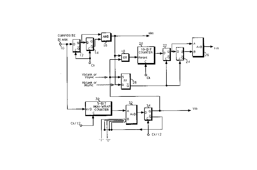
FIGURE 1 illustrates an embodiment of the oddteven
field detector as it may be implemented in a Pix-in-Pix system for
determining the respective fields of, for example, the main video
signal. In this instance field determination is derived from a
15 composite blanking signal provided by the main signal processing
circuitry (not shown). The relative timing between .he vertical
and horizontal blanking intervals of a given video signal may not
conform to any standard. However for an interlaced signal the
vertical synchronizing (and thus blanking) pulses for consecutive
2 0 fields must have a one-half horizontal line period timing
difference relative to the horizontal synchronizing (blanking
pulses .
In a Pix-in-Pix system one may associate odd/even
field designation with respective spatial placement within a raster
25 (i.e., line one of odd ffelds falls spatially above line one of even
fields when the signal is applied to a television raster). This type
of field distinction is completely dependent upon the selection of
line number one within the two consecutive fields.
The primary purpose of Pix-in-Pix systems is to
30 synchronize an auxiliary video signal to be displayed as an inset
in a main image (derived from a main video signal) with the main
video signal. Nominally this is accomplished by storing the
auxiliary video signal in memory synchronously with the auxiliary
video signal, and thereafter reading the auxiliary video signal
35 from memory synchronously with the horizontal and vertical
timing components of the main video signal. The circuitry of
FIGURE 1 develops the horizontal and vertical timing pulses Hm
and Vm from the main composite blanking signal for use by the
R CA 8 5 ,987 ,~ J~
-3 -
Pix-in-Pix system, and also develops a field identification signal
Fm for use by the Pix-in-Pix interlace control system. Elements
18-28 of the FIGURE 1 circuitry generate the field identification
signal Fm from the horizontal and vertical timing signals Hm and
5 Vm.
Referring to FIGURES 1 AND 2, figures 2A and 2F
illustrate portions of exemplary composite blanking signals for
successive even and odd fields respectively. For the illustrated
waveforms~ even and odd fields are defined according to whether
10 the time (thus spatial) period between the end of vertical
blanking and the horizontal blanking pulse representing line
number one of the field is long or short relative to that same
measurement made on the previous field.
The composite blanking signal is applied to terminal
1 0 and coupled to the circuitry including elements 1 2- 1 6 which
generate a horizontal timing signal Hm. Elements 12-16 comprise
a positive going transition detector and develop a pulse one clock
period wide on the occurrence of each positive going transition of
the composite blanking signal as follows. Elements 12 and 14 are
20 D-type latches which are clocked by a signal Ck having a
frequency of, for example, four times the color subcarrier
frequency. A D-type latch provides, at its Q output terminal, the
logic value present at its data input terminal D, immediately
before the occurrence of a pulse applied to its clock input terminal
25 C. The composite blanking signal is applied to the data input
terminal of latch 12, the output terminal, Q, of which is coupled to
the data input terminal of latch 14. The Q output terminal of latch
12 and the Q output terminal of latch 14 are coupled to
respective input terminals of an AND circuit 16. The Q output of
30 latch 12 corresponds to the composite blanking signal. The Q
output of latch 14 corresponds to the composite blanking signal
delayed by one clock, Ck, period and inverted in polarity. AND
gate 16 provides _logic one output value when the Q output of
latch 12 and the Q output of latch 14 are both logic one values,
3 5 which only occurs for one clock period immediately following a
positive transition of the composite video signal. The output
signal Hm provided by the AND gate 16 is illustrated in FIGURES
2B AND 2G.
RCA 85,98~ ~3 ~
-4 -
The composite blanking signal is also coupled to the
circuitry including elements 30-34 which generates the vertical
timing signal Vm. The signal Vm is normally low valued and goes
high a predetermined interval after the positive transition of the
vertical component of the blanking signal and then goes low
subsequent the end of the vertical blanking interval.
Elements 30-34 operate as follows. Element 30 is an
up/down counter having the composite blanking signal coupled as
an up/down control signal to its U/D control input terminal. The
1 0 up/down counter 30 counts pulses of a clock signal Ck/12 having
a frequency of, for example, one-third the frequency of a color
subcarrier signal. Counter 30 provides count values between zero
and thirty-one inclusive and is arranged so that it does not wrap
around. That is, if the counter is counting up (down) and the
1 5 number of clock pulses occurring before the counter is conditioned
to count down (up) is in excess of the number necessary to
condition the counter to provide its maximum (minimum) count
value of 31(0), the counter will continue to output its maximum
(minimum) count value of 31(0) for each clock pulse in excess.
2 0 Counter 30 effectively operates an an integrator having an output
which saturates in both the positive and negative going directions.
The output of the up/down counter 30, which is a five bit signal,
is coupled to one input of a comparator circuit 32. A reference
value is coupled a second input of the comparator circuit 32.
Comparator circuit 32 provides a logic one signal only when the
output count from the counter 30 exceeds the reference value.
The output signal from the comparator 32 is applied to the data
input terminal of a D-type latch 34 which is clocked by the clock
signal Ck/12, and provides the signal Vm at its Q output terminal.
The reference value and the frequency of the clock
signal applied in the counter 30 are selected so that the value
output by the counter 30 will not exceed the reference value
during horizontal blanking periods. Thus the Q output of latch 34
will exhibit a logic low value during occurrences of horizontal
blanking pulses. In the illustrated embodiment of FIGURE 1, the
reference value is 11011 (binary) or 27 decimal, and is arranged
- to be dynamic to provide system hysteresis. Note that the most
significant and third most significant bits of the reference signal
RCA 85,987
S
applied to the B input terminal of the comparator 32 are 2 ~
respectively coupled to logic "1" and "0" values. The remaining
bits of the reference value are coupled to the Q output of the
latch 34. Assumin_that comparator 32 has been producing low
5 output values, the Q output of latch 34 will exhibit a logic high
state and the reference value is 11011 (binary). After the output
of comparator 32 goes high, the Q output of latch 34 exhibits a
low value, changing the reference value of 10000 (binary) or 16
decimal. If there is some noise in the vertical blanking interval,
1 0 causing the counter to oscillate between up and down counts,
reducing the reference value precludes the output signal provided
by the latch 34 from changing state prematurely.
The counter 30 counts up for high levels of composite
blanking and counts down for low levels. Nominally the counter
1 5 30 will exhibit a zero value in approximately 12 llsec or less after
termination of each horizontal blanking interval because the
typical horizontal blanking pulse is 12 ~lsec wide and the counter
will count down in a time equivalent to the horizontal blanking
pulse width. Assuming that the counter 30 exhibits a zero value
2 0 on the occurrence of a vertical blanking pulse, latch 34 will exhibit
a high output state approximately 23.5 ~sec (28 clock cycles each
having a period of 840 ns) after the positive going transition of
the vertical blanking interval. Alternatively, if the last horizontal
blanking pulse before the occurrence of the vertical blanking
2 5 interval is relatively close to the vertical blanking interval, the
counter 30 may exhibit a value other than zero at the start of the
vertical blanking interval. In this instance the leading edge of the
signal Vm will be spaced less than 23.5 ~,Isec from the leading edge
of the vertical blanking interval. This however is of no
30 consequence. The signal Vm goes low 12.6 ~,Isec after the
termination of the vertical blanking interval, i.e., the counter must
count down from 31 to 16 (15 x 840 ns) for the comparator to
change state. However, if the end of the vertical blanking interval
is relatively close to the first subsequent blanking pulse, i.e.,
3 5 within a period corresponding to less than 15 cycles of the clock
Ck/12, the signal Vm will remain high for a period of 15 cycles of
the clock Ck/12 following the first subsequent horizontal blanking
pulse. This may be seen with reference to FIGURES 2F and 2H.
- 6 - RCA 85,987 ~ 3
Note however that the trailing edge of the signal Vm may be
conditioned to substantially conform to the end of the vertical
blanking interval, if desired, by eliminating or reducing the
amount of hysteresis applied to the reference value applied to the
comparator 32.
Refer to elements 18-28 which generate the odd/even
field signal Fm. Elements 18-28 are arranged to develop a count
value proportional to the time elapsed from the negative going
transition of the signal Vm to the occurrence of the first
1 0 subsequent pulse of the signal Hm in each field, and to compare
the count values from successive fields. Because the interval
between the negative going transition of the vertical blanking
interval and the occurrence of the first subsequent horizontal
blanking pulse differs by approximately one-half of one horizontal
1 5 line interval in successive fields, the respective count values for
odd and even fields will differ significantly. A comparison of the
count value of the current field with the count value of the
previous field will provide an indication of whether the current
field is odd or even.
In FIGURE 1 a 10-bit counter 20 counts pulses of the
clock signal Ck. The counter 20 is reset to zero by the signals Hm
and Vm which are applied to a reset terminal via a logic OR circuit
18. (Note that the signal Hm need not be applied to the reset
terminal of the counter 20 for the purpose of generating the signal
Fm. However, if the signal Hm is applied to reset counter 20, then
the output of counter 20 can serve as, e.g., a pixel address counter
in a Pix-in-Pix system, during the non-vertical blanking intervals
of each video field.) The counter 20 is maintained in the reset
state for the interval that the signal Vm exhibits a high state and
begins counting immediately following the negative going
transition of the signal Vm. Count values provided by counter 20
are coupled to a D-type latch 22 which is conditioned by a control
signal developed by element 28, to store the count value present
on the occurrence of the first subsequent horizontal blanking
pulse following the negative going transition of the signal Vm.
The output of the D-type latch 22 is coupled to a further D-type
latch 24 which is clocked simultaneously with the latch 22.
Latches 22 and 24 contain the count values for the current and
RCA 85,987 2 ~
previous fields respectively. The count values stored in latches 22
and 24 are respectively coupled to the A and B input terminals of
a comparing circuit 26. Comparing circuit 26 exhibits high and
low output states for the count value applied to its input terminal
5 A being greater and lesser respectively than the count value
applied to its terminal B. With knowledge of the relative timing of
the vertical blanking interval to the first subsequent horizontal
blanking pulse from field to field, the designer can designate
whether the high or low output state exhibited by the comparing
10 circuit 26 corresponds to an odd or an even field. The signal Fm is
illustrated in FIGURE 2E and 2K for two successive field periods.
Control signals for clocking the latches 22 and 24 are
developed by a set-reset flip-flop 28 which is of the type wherein
the set input signal has precedence over a concurrently applied
15 reset signal. That is, as long as a logic high signal is applied to the
set input terminal of the flip-flop, the flip-flop will remain in the
set state regardless of the signal level applied to its reset input
terminal .
The control signal is taken from the Q output
20 terminal of flip-flop 28. Thus when the flip-flop is in the reset
(set) state the control signal is a logic high (low) level. With
respect to latches 22 and 24, the operative portions of the control
signal are positive going transitions.
The signal Vm is applied to the set input terminal of
25 flip-flop 28 and the signal Hm is applied to its reset terminal. The
flip-flop is reset at the occurrence of the first horizontal blanking
pulse subsequent the negative going transition of the signal Vm.
Flip-flop 28 remains in the reset state and exhibits a logic high
output state until the occurrence of the positive transition of the
3 0 signal Vm, at which time it exhibits a logic low state. The flip-flop
is constrained to remain in the set state for the duration that the
signal Vm exhibits a high state. Thereafter on the occurrence of
the next pulse of signal Hm it is reset. The control signal provided
by flip-flop 28 iS illustrated in FIGURES 2D and 2J for two
35 successive fields.
If the signal Hm is applied to the reset input terminal
of the counter 20, it may be necessary to delay the signal Hm
applied to the OR circuit 18 relative to the signal Hm applied to
RCA 85,987
- 8 -
the flip-flop 28 to insure that the count value provided by counter
20 is stored in latch 22 before the counter 20 is reset.
As shown in FIGURE 1 and discussed herein the signal
Fm is developed from a composite blanking signal with the aid of
S circuit elements 12-16 which provide a horizontal timing signal
and elements 30-34 which provide a vertical timing signal related
to horizontal and vertical blanking pulses respectively. However,
if separate horizontal and vertical blanking signals (Hblank~
V blank) are available from standard blanking signal generators,
10 they may be coupled directly to circuit elements 18 and 28 as
indicated in phantom in FIGURE 1. Alternatively, if horizontal
synchronizing signals HSync and vertical synchronizing signals
V sync are available from standard sync separators, they may be
utilized to develop an odd/even field signal Fm by connecting
15 these signals directly to elements 1 8 and 28 as indicated. The
only constraints on these signals that are necessary for the
elements 18-28 to develop a field indicating signal are that the
time interval between Vblank (Vsync) and the occurrence of the
first subsequent Hblank (HSYSC) pulse be relatively constant in
2 0 respective odd and even fields and be different between
successive fields.
~ . .