Note : Les descriptions sont présentées dans la langue officielle dans laquelle elles ont été soumises.
Cf~
C FO 7 513 v-S--
- 1 -
1 Information Transfer Method, Information Transfer
Apparatus, and its Driving Method
BACKGROUND OF THE INVENTION
Field of the Invention
This invention relates to an information
transfer method of an image information in, for
example, still video, etc., an information transfer
apparatus, and its driving method.
Also the present invention pertains to an
information transfer apparatus to be applied to, for
example, still video apparatus, copying machine, etc.
Related Background Art
In the prior art, MIM device (switching LB-MIM
device) having switching memory function with an LB
film (Langmuir-Blodgett's film) as the insulation film
has been proposed in Japanese Patent Application Laid-
open No. 63-96956.
About how the devices by use of such LB film ,
can be specifically incorporated into the system in
order to surpass the group of apparatus related to
electronics techniques which have been developed with
inorganic semiconductors as the center in the przor -
art, the study is still at the stage when just begun.
As an example, there may be only mentioned the
tact that great memory ability can be exhibited by
- 2 -
1 making an access of an organic thin film having
switching memory function by an STM apparatus as
proposed in Japanese Patent Application Laid-open No.
63-161553.
One of the specific features of such organic
thin film is that a large area can be prepared more
unifarmly as compared with inorganic semiconductors,
but even if a thin .film with any large area can be
formed and may potentially have great memory, without
an appropriate access means, no practically great
memory ability can be exhibited.
As an example conceivable as the access means,
there may be mentioned an example in which matrix
circuits are assembled and the respective intersecting
points of the matrix are used a~~ memory.
However, in such case, the memory capacity
obtained is only about square of the number of wirings
from outside.
On the other hand, there has been proposed the
2p charge transfer system known as the bucket brigade
device (abbreviated as BBD) in which charging and
discharging of capacitor are performed every other
bit, in Sangster, F. J., Philips Tech. Review 31 92-
110 (190).
However, in such information transfer system
(method), when the power voltage is made OFF state,
__
1 the capacitor discharges the charges with time,
whereby there has been involved that no information
can be memoried for a long time within BBD.
SUMMARY OF THE INVENTION
Accordingly, an object of the present
invention is to provide an information transfer
method, an information transfer device and a driving
method thereof which can store information semi-
permanently even if placed under OFF state which has
cancelled the problems as described above.
Another object of the present invention is to
provide an information transfer apparatus of a new
type which can draw out potentially great memory
capacity based on large area of organic thin film,
having high capacity as well as high reliability and
yet is excellent in bulk productivity with small
number of wirings from outside.
The above objects can be accomplished by the
present invention as specified below.
In the first place, there is provided an
information transfer method, which comprises
connecting a plurality of MIM devices comprising a
monomolecular film of an organic compound or built-up
films thereof as the insulating layer and having the
switching memory function, and transferring the
- 4 -
1 information on the side nearer to the oscillation
source of the information every second bit or every
second line or every second picture face successively
to the side farther from the oscillation source.
Secondly, there is provided an information
transferring method, which comprises transferring an
information in an electrical circuit having a devices
and b devices which are MIM devices comprising a
monomolecular film of an organic compound or built-up
lp films thereof as the insulating layer and having the
switching memory function arrayed alternately in a row
or in a plurality of rows, wherein the memory in the b
devices is erased to effect information transmission
from the a devices positioned immediately before said
b device to said b device, and subsequently the memory
in the a device is erased to effect information
transmission from the b device positioned immediately
before said a devioe to said a device.
Thirdly, there is provided an information
transfer apparatus comprising using an array or a
plurality of arrays of circuits with devices having
rectifiability connected in series with the rectifying
directions being aligned, connecting one terminal of a
two-terminal circuit having an MIM device having
switching memory function to each connecting point A,
connecting the other therminal of every odd number -to
- 5 -
1 provide a second terminal, and having a voltage
application means capable of taking a disconnected
state relative to said connecting point A.
Fourthly, there is provided a method for
driving an information transfer apparatus according to
the second or the third invention, which comprises, as
the first period, applying a voltage for making the
MIM device of the information transfer address under
the first state simultaneously with holding the
information of the MIM device of the information
transfer source and, as the second period, a voltage
for information transfer is applied.
Fifthly, there is provided an information
transfer apparatus comprising an MIM device comprising
a monomolecular film of an organic compound or a built-
up film thereof as the insulating film, a circuit
having a device of which electrical resistance varied
depending on the input information connected and a
voltage application means.
Sixthly, there is provided an information
transfer apparatus, comprising an MIM device
comprising a monomolecular film of an organic compound
or built-up films thereof as the insulating film and
having the switching memory function at each
connecting point of a circuit with devices having
rectifiability connected with their rectifying
- 6 -
1 directions aligned, a circuit with a device of which
electrical resistance varies depending on the input
information arranged on one end thereof and a resistor
on the other end, respectively, and a voltage
application means.
Seventhly, there is provided an information
transfer apparatus comprising an MTM device comprising
a monomolecular film of an organic compound or built-
up films thereof as the insulating layer and having
switching memory function, a circuit having a device
of which electrical resistance varies with temperature
connected thereto and a voltage application means.
Eighthly, there is provided an informatian
transfer apparatus, comprising an MTM device
comprising a monomolecular film of an organic compound
or built-up films thereof as thee insulating film and
having the switching memory function arranged at each
connecting point of a circuit with devices having
rectifiability connected with their rectifying
directions aligned, a circuit with a device of which
electrical resistance varies with temperature arranged
on one end thereof and a resistor on the other end,
respectively, and a voltage application means.
Ninthly, there is provided an information
transfer apparatus comprising an MTM device comprising
a monomolecular film of an organic compound or built-
1 up films thereof as the insulating layer and having
switching memory function, a circuit having a
photoconductive device connected 'thereto and a voltage
application means.
Tenthly, there is provided an information
transfer apparatus, comprising an M1M device
comprising a monomolecular film of an organic compound
or built-up films thereof as the insulating film and
having the switching memory function arranged at each
connecting point of a circuit with devices having
rectifiability connected with their rectifying
directions aligned, a circuit with a photoconductive
arranged on one end thereof and a resistor on the
other end, respectively, and a voltage application
means.
Eleventhly, there is provided an information
transfer apparatus, comprising an MIM device
comprising a monomolecular film of an organic compound
or built-up films thereof as the insulating film and
having the switching memory function arranged at each
connecting point of a circuit with devices having
rectifiability connected with their rectifying
directions aligned, a circuit with a photooonductive
arranged on one end thereof and a resistor on the
other end, resepctively, a voltage application means,
an information holding member having an image
_ g _.
1 information, a movement amount detecting device for
detecting the movement amount of said information
holding member, a linear light source and an optical
system for inputting the image information into the
photoconductive device by reflecting the light from
said linear light source.
Twelfthly, there is provided an information
transfer apparatus, comprising a monomolecular film of
an organic compound or built-up films thereof as the
insulating layer and having switching memory function,
a circuit having a device of which electrical
resistance varies with humidity connected thereto and
a voltage application means.
Thirteenthly, there is provided an information
transfer apparatus, comprising an MIM device
comprising a monomolecular film of an organic compound
or built-up films thereof as the insulating film arid
having the switching memory function arranged at each
connecting point of a circuit with devices having
rectifiability connected with their rectifying
directions aligned, a circuit with a device of which
electrical resistance varies with humidity arranged on
one end thereof and a resistor on the other end,
respectively, and a voltage application means.
BRIEF' DESCRIPTION OF THE DRAWINGS
_ g ._
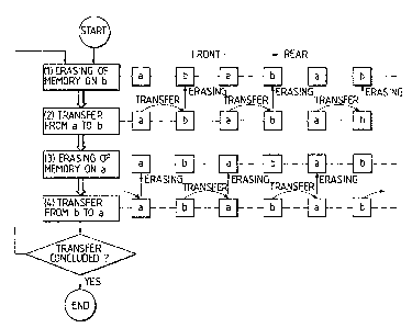
1 Fig. 1 is a diagram showing an example of the
informatiora transfer method of the present invention.
Fig. 2 is a graph showing the characteristics
(I-V characteristics) of the switching memorizable MIM
device.
Fig. 3A is a circuit diagram showing an
example of the information transfer apparatus of the
present invention.
Fig. 3B is a diagram showing an example of the
driving method of the information transfer apparatus
of the present invention.
Figs. 4A and 4B are diagrams for illustration of
the principle of the information transfer apparatus.
Figs. 5A - 5D are diagrams for illustration of
the principle of information transfer.
Fig. 6 is a diagram showing the basic
constitution of the apparatus according to another
embodiment of the present invention.
Fig. ~ is a constitutional view showing an
example of the present invention.
Fig. 8 is a diagram for illustration of the
application states of the voltages V1, V2, V3 used in
the example.
Fig. 9 is a diagram showing the basic
constitution of 'the apparatus according to another
embodiment of the present invention.
_ 10 __
1 Fig. 10 is a constitutional view showing
another embodiment of 'the present invention.
Fig. 11 is a constitutional view showing
another embodiment of the present invention.
Fig. 12 is a diagram showing the basic
constitution of the apparatus according to another
embodiment of the present invention.
DETAILED DESCRITPION OF TFiE PREFERRED EMBODIMENTS
More specifically, according to the present
invention, by use of an MIM device having switching
memory function with a monomolecular film of an
organic compound or built-up films thereof as 'the
insulation layer (switching LB-MIM device), the
information in the front is successively transfer
memoried at every another bit or every another line or
every another picture face, successively, to the rear,
whereby the information is adapted to be stored semi-
permanently within the switching hB-MIM device even
the power source voltage may be made OFF state.
Further, according to the present invention,
by applying a voltage on a circuit connected in series
- with an MIM device having switching memory function
(switching LB-MIM device) as described above and a
device of which electrical resistance varies depending
on the input information, the input information can be
a
~~~n~~
- 11 -
1 transferred to the switching LH-MIM device to be
memoried therein, and the memoried information will be
stored semi-permanently even if the power voltage may
be made O~'F' state.
The input information as mentioned in the
present invention refers to temperature. humidity,
light, etc.
The switching memory function as mentioned in
the present invention refers to the function of
enabling reversibly transition (switching) to the low
resistance state and the high resistance state and yet
capable of holding (memorying) the respective states
even when application of voltage may be stopped by
applying a voltage exceeding the threshold value
capable of transitioning the state' exhibiting two or
more electroconductivities differsant from each other
under the state where a thin film such as an organic
monomolecular film, built-up filme> thereof, et.c. is
arranged between a pair of electrodes.
In such present invention, applicable organic
compounds may include organic materials having a group
having ~z~-electron conjugation system which system is
suitable for the present invention, and examples of
the structure of the dye having the r~-electron
oon3ugation system may include dyes having porphyrin
slcelton such as phthalocyanine, tetraphenyl-
~- 12 -
1 porphyrin, etc., azulene type dyes having squarylium
group and croconicmethine group as the linking chain
and dyes analogous to cyanine type having 2 nitrogen
containing heterocyclic rings such as quinoline,
benzothiazole, benzooxazole bonded through squarylium
group and croconicmethine group, or fused polycyclic
aromatic compounds such as cyanine dyes, anthracene
and pyrene, etc., and linear compounds comprising
polymers of aromatic and heterocyclic compounds and
1d polymers of diacetylene groups, furfiher derivatives of
tetracynoquinodimethane or tetrathiafluvalene and
anal4gues thereof and charge transfer complexes
thereof, and further metal complex compounds such as
ferrocene, ~tris'bipyridine luthenium complexes, etc.
f1s the polymeric material suitable for the
present invention, for example, there may be included
biological polymers of addition polymers such as
polyacrylic acid derivatives, etc., condensed polymers
such as polyimide, etc., ring-opened polymers Such as
nylon, etc.
Concerning formation of the above insulation
layer, although specifically the vapor deposition
- method, the cluster ion beam method, etc. can be
applied, the Langmuir-Slodgett°s (LB) method may be
extremely suitably employed for controllability,
easiness and reproducibility.
~~~u
- 13 -
1_ According to the LB method, a monomolecular
film of an organic compound having hydrophobic sites
and hydrophilic sites in one molecule or built-up
films thereof can be formed easily on a substrate, and
also a uniform, homogeneous organic ultra-thin film
having a thickness of molecular order and over a large
area can be stably supplied.
The LB method is a method for forming a
monomolecular film or built-up films thereof by
utilizing the fact that when in a molecule with a
structure having hydrophilic sites and hydrophobic
sites, when the balance between the bona (amphiphilic
balance) is adequately maintained, the molecule will
become a layer of monomalecular film with the
hydrophilic groups directed downwardly.
As the group for constituting the hydrophobic
mites, there may be included various hydrophobic
groups generally and.widely known in the art such as
saturated and unsaturated hydrocarbon groups or fused
polycyclic aromatic groups and chain polycyclic phenyl
groups, etc. These will constitute the hydrophobic
sites individually or as a combination of a plurality
' thereof. On the other hand, as the most
representative of the constituents of hydrophobic
sites, there may be included hydrophilic groups suoh
as carboxyl group, ester group, acid amide group,
~~i~~~
- 14 -
1 imide group, hydroxyl group, further amino groups
(primary, secondary, tertiary and quaternary).
An organic molecule having these hydrophobic
groups and hydrophilic groups in combination with good
balance can form a monomolecular film on the water
surface, and can be an extremely suitable material for
the present invention,
The switching memory characteristic of the
compounds having these ~t-electron conjugation systems
lp can be observed even with a film thickness of some 10
nm or less, but the thickness should be preferably
made 5 to 30~ a from film forming property,
uniformity, etc.
As the electrode material constituting the MIM
device, it is preferably formed of noble metals such
as Au, Pt, Pd, etc. which will not form insulating
oxides on the electrodes (generally electrodes
deposited on the support substrate) on which
monomo,lecular film or built-up films thereof axe
2~ formed, or electroconductive oxides such as ITO, etc.
Referring now to Examples, the pressnt
invention is described in detail.
Example 1
Fig. 1 is a diagram showing best the specific
features of the information transfer method which is
the present invention, particularly an information
~~3~r~~i
7. 5 -.
1 tran.~-afer method in an electrical circuit with a
devices and b devices which are switching LB-MIM
devices of the same kind being juxtaposed in a row in
the order of ... ababab...(or a plurality of rows),
characterized in that:
(1) first, the memory of a b device is erased,
(2) an information is transferred from an a
device to the adjoining rear b device,
(3) subsequently, the memory in the a device
is erased, and
(4) an information is transferred from the b
device to the adjoining rear a device.
Here, as the a device and the b device, as
shown in Fig. 6, 11, a switching LB-MIM device having
a constitution of (upper electrode) 16/SOAZ
(squarylium type dye) layer LB :film 15/Au (lower
electrode) 16 were employed.
Such MIM device was prepared as described
below.
First, on a glass substrate 1Z (#059 produced
by Corning) subjected to the hydrophobic treatment by
leaving it to stand in the saturated vapor of
hexamethyldisilazane (HMDS) one day and night was
deposited Cr as the subbing layer to a thickness of
500 A by the vacuum vapor deposition method, further
vapor deposited Au (film thickness 1000 ~.) by the same
- 16 w
1 method to form a stripe-shaped subbing electrode 16 to
a width of 1 mm. By use of such substrate as the
carrier, monomolecular films of squarylium-bis-6-octyl-
azulene (SOAZ) were built up by the LB method. The
method for building up films is described in detail
below.
A solution of SOAZ dissolved at a
concentration of 0.2 mg/ml in chloroform was spread
onto an aqueous phase with a water temperature of 20
oC to form a monomolecular film on the water surface.
Having awaited evaporation of the solvent, 'the surface
pressure of the monomolecular film was enhanced to 20
mN/m, and further the above substrate was dipped in
the direction transversing the 'water surface gently at
a speed of 10 mm/min., and subsequently drawn up
gently at 5 mm/min. to build up two layers of Y-type
monomolecular films. Then, this was repeated to build
up 12 layers, thus forming an insulating layer (LB
film) 15.
Next, on such film surface is vacuum vapor
deposited a stripe-shaped A1 (film thickness 1500 A)
with a width of 1 mm so ws to be crossed at right
angle, while maintaining the substrate temperature at
room temperature or lower, to form an upper electrode
16.
Fig. 2 shows the switching memory
- 17 -
1 characteristics (I-V characteristics) of this device.
Switching hB-MIM devices generally take three states
with different electroconductivities of OFF state [OFF
(Bj state], MID state [OFF (A) state) and UN state,
but here, the specific feature resides in use of the
switching memory function between the OFF (B) state
and the OFF (A) state. Of course, the present
invention is not limited to this, but, fox example,
the switching memory function between OFF (B) state
and ON state may be also employed.
As shown in Fig. 2, such MIM device 11 has
switching memory characteristics having OFF (A) state
and OFF (B) state and, particularly around 2 V of
application voltage, OFF (A) state (state "1") is a
resistance value of KS2 order and OFF (B) state (state
"0" ) that of MS2 order.
Switching from the state "1" to tha state "O"
is effected by application of rectangular pulses of 5
V or higher, and the switching from the state "0" to
the state "1" by application of rectangular pulses o.f
about 3 V.
In Fig. 1, information transfer from the a
' device to the b device is effected particularly by
switching so that the b device may become also the OFF
(A) state if the a device is OFF {A) state, and the b
device may become also the OFF (B) state if the a
- 18 -
1 device is OFF (B) state.
Example 2
Fig. 3A is a diagram showing an example of the
information transfer apparatus which is the present
invention, and it is an information transfer apparatus
by use of an array (or a plurality of arrays) of a
circuit with devices 51 to 56 having rectifiability
connected in series, characterized in that one
terminal of the two-'terminal circuit having the
switching LB-MTM devices 61 to 66 is connected to each
connecting point A, and that the other device at the
odd number is connected to provide a first terminal 1
and that at the even number is connected to provide a
second terminal 2, and that the apparatus has a
voltage application means capable of taking the
disconnected state relative to the above connecting
point A.
In Fig. 3A, 4 is a switch enabling the
disconnected state, and here particularly a
photocoupler switch was employed, but, for example, a
conventional electromagnetic system relay may be also
employed. 3 is the terminal for applying a voltage an
- the connecting point A.
Now, in Fig. 3A, when voltages having
polarities different from each other are applied on
the first terminal 1 and the second terminal 2, due to
_ 19 _
1 the function of the device having rectifiability, as
shown in Figs. 4A and 4B, the partion applied with the
voltage of the opposite direction to rectifiability
becomes severed state, and only the portion applied
with the voltage of the same direction as
rectifiability is connected. That is, a circuit
comprising a pair of each two of the switching LB-MIM
devices of (+)switching LB-MIM device/device having
rectifiability/(-) switching LB-MIM device is formed,
and 'the information is transferred from the front
device of said pair to the rear device. However, fox
the information to be correctly transferred, prior to
information transfer, it becomes necessary to make the
switching LB-MIM device of the information transfer
address OFF state (the first state or OFF (B) state)
and at the same time hold the information of the
switching LB-MIM device of the information transfer
source by use of the voltage application means capable
of taking the disconnected states comprising 3 and 4
and the first terminal 1 and the second terminal 2.
Figs. 5A - 5D are diagrams for illustratiow of
the calculation function and the information transfer
function when a voltage was applied on the a devices
and the b devices having the characteristics shown in
Fig. 2 connected in series, 5A showing a circuit
diagram, 5B a truth table, 5C a chart showing that
- 20 -
1 when a voltage is applied on a circuit having devices
of OFF (A) state [state "1°'] and OFF (B) state [state
"0"] connected in series, most of the voltage is
applied to the OFF (B) state, 5D a chart that when a
voltage is applied on a circuit having devices of OFF
(B) state [state "0"] and OFF (B) state [state "0"],
only half voltage (V/2) of the applied voltage (V) is
applied on the respective devices.
For switching the characteristics shown in
Fig. 2 from the OFF (A) state to the OFF (B) state,
the application voltage may be abruptly blocked by
application of a voltage of about 5 V or higher, while
an the contrary switching from the OFF (B) state to
the OFF (A) state effected by application of a voltage
of about 3 V.
Therefore, by application of pulses with a
peak voltage of about 3 V, it becomes possible to
carry out the calculation processing having the a -~ b
(OR) function as shown in Fig. 5B. Hence, by using
the b device side as constantly reset to the OFF (B)
state [state '°0"], the information of the a device can
be transferred to the b device.
Example 3
Fig. 3B is a diagram showing an example of the
driving method of the information transfer device of
the present invention.
2~~~~~~
- 21 -
1 As shown in 'the diagram, the method as the
specific features in that it has the first period '11
and the second period Z2, and in the first period, the
switching LB-M3M device of the information transfer
address is made the off-state (the first state of the
OFF (B) state) and at the same time the voltage for
holding the information in the switching LB-MIM device
of the information transfer source is applied, while
in the second period, the voltage for information
transfer is applied.
Particularly, here, the apparatus is
characterized by using the switching memory function
between the OFF (B) state and the OFF (A) state of the
switching LB-MTM device. Fig. 3B is a time chart of
the voltage waveforms during application of the
voltages V1, V2, V3 respectively on the terminals 1,
2, 3, with 1H=80 msec, 1F=2H being the repetition (1
cycle) units, and by applying repeatedly waveforms
corresponding to 1F, the information within the
information transfer apparatus shown in Fig. 3A will
be gradually transferred.
Here, particularly the peak voltages of V1 and
V2 in the first period were made *4V and ~ ~V, and the
peak voltage of V3 was made - 4V. On the other hand,
the peak voltages of V1 and V2 in the second period
were made ~ 1.8V and + 1.8V, and V3 floating by
_. 2 2
1 disconnection with the switch 4. Particularly, as the
diodes 51 to 56, a silicon diode with a holding
voltage of 0.? V in the normal direction was employed.
Therefore, in the first period within the initial 1H
period, the voltage (V3-V1) applied on the devices 61,
62, 63 become 0 V, whereby the infarmations are held,
while the voltage (V3-V1) applied on the devices 62,
64, 66 become 8 (=4.+4) V, whereby resetting to the OFF
(H) state is effected due to stand-up in shape of
pulses. In the second period within the initial 1H
period, the circuit state as shown in Fig. 4A is
formed, and on the devices 62, 6.4, 65, if 61, 63, 66
of the information transfer sources are OFF (A) state,
pulse voltages having a peak voltage of about V1 + V2 -
VF = 3.1V are applied, whereby 62, 64, 65 became also
OFF (A) state. On the contrary, if 61, 63, 66 of the
information transfer sources are OFF (B) state,
triangular waves having a peak voltage of about (V1 +
V2 -~ VF)/2 ~' 1.5V are applied, whereby OFF (H) state
remains as such because the value is lower than the
switching threshold value. ~'hus, information is
transferred and memoried between 61 ~ 62, 63 -> 64, 65
66.
Similarly in the next 1H, information between
62 -> 63, 64. ~ 65 are transfer memoried, and
subsequently transfer and memory of information were
- 23 -
1 successively performed by repeated pulses.
B~tample 4
Fig. 6 is a schematic constitutional view
showing another embodiment of the information transfer
device of the present invention, wherein 11 is the MIM
device (switching LB-MIM device) used in Example 1, 12
a device of which electrical resistance varies with
temperature, and 13 is a voltage application means.
Here, as the device 12, particularly a CTR-
type temperature sensitive semiconductor utilizing a
weakly reducible atmosphere sintered product of a VBaP
mixture oxide was employed.
The device 2 of which electrical. resistance
varies with temperature exhibited a law resistance
value of about 50SZ under the high temperature state
(state "1") with a temperature of 100 oC, and had a
high resistance value of about 1 MS2 under the low
temperature state (state "0°') with a temperature of 0
oC.
Therefore, in Fig. 6, under 'the state of the
switching LB-MIM device 1 rest at the OFF (B) state,
by applyf~ag driving pulses with a poise width of 1
sec., a peak voltage of 3 V by use of a voltage
application means 13, when the device 12 is under the
high temperature state (state "1"), most of the
application voltage is agplied on the MIM device 11,
- 2~ -
1 whereby such MIM device 11 can be made OFF (A) state
(state "1"), while when the device 12 is under the low
temperature state (state "0"), the application voltage
is divided by resistance to be applied on the MTM
device 11, whereby such MIM device 11 can be held as
such under the OFF (B) state (state "0").
Thus, the temperature information possessed by
the device 112 of which resistance varies with
temperature could be transfer memoried to the
switching LB-MIN device 11.
Example 5
Fig. T is a diagram showing another example of
the present invention. In the present example, the
information transfer apparatus is characterized by
using a circuit B in which switching LB-MTM devices 32
to 3T are arranged at the respective connecting points
A of the circuit with the diode deavices 21 to 2T
connected in series with the rectifying directions
aligned from the front top to the rear tail, the
device 31 of which resistance varies with temperature
is arranged at the front top of the above circuit and
the resistor 38 arranged at the rear tail of the above
circuit.
By use of such circuit B, the temperature
information detected by the device 31 as transferred
successively in the rectifying direction of the diodes
1 to be memoried, and by monitoring -the voltage at both
terminals of the resistor at the rear tails, it has
become possible to read the information transfer
mernoried. In the following, detailed description is
made.
In Fig. T, 41 and 42 are voltage application
means V1 arid V2 primarily for information transfer, 43
is voltage application means V3 primarily making the
device which becomes the information transfer address
among 32 to 3? OFF (B) state (state "0"), and 44 relay
switch for making the voltage application means 43
disconnected state relative to the connecting point A
during information 'transfer.
In such apparatus, by applying repeatedly a
voltage characterized by having tine first period ?1
and the second period ?2, different polarities at V1
and V2 from each other and the abscolute values V1, V2,
V3 of the first interval voltage being equal to each
other, as the power sources V1, V2, V3 in Fig. ? as
shown in Fig. 8, transfer recording of information is
effected. Here, particularly the resistance of the
device 3l ~axzder low temperature state, the resistance
- of the switching LB-MIM devices 21 to 2? under OFF (B)
state, and the resistance of the resistor at the
circuit terminal are all equal on the MS2 order, and as
the diodes 21 to 2?, silicone diodes were employed,
- zs -
1 and as the maintained voltage VF in the normal
direction, O.Z V, while in the opposite direction, one
with s~zfficiently high resistance than MS2 were
employed.
At this time. when the peak voltage in the
first section is wade ~ 4V, and the switch ~4
connected state, there is realized the state that
every another of the diodes 2:t to 2T is applied with a
voltage of V1 - V2 = + 8V, while no voltage is applied
on other devices. In this case, the switching LB-MIM
device applied with a voltage of + 8V is reset to the
OFF (B) state, to be ready as the information transfex
address. On the other hand, the device applied with
no voltage continues to hold the information to become
the information transfer source.
Next, by making the peak voltages of V1, V2 in
the second section + 1.~ V, and V;3 disconnected state
by use of the .relay switch 44, a <:ircuit of high
independency is formed between the LB-MIM device of
the information transfer source, the diodes in the
normal direction and the LB-MIM device of the
information address (or resistor at terminal), whereby
a voltage of 8.1 (=~.8 - O.T)V excluding the
maintained voltage VF (=0.7 V) is applied on the
series circuit of LB-MIM and therefore information and
recording (excluding resistor at terminal) are
- 2'I -
1 effected according to the same principle as in Example
4. Accordingly, by applying repeatedly the waveform
as described above while varying alternately the
polarities of V1 and V2, the temperature information
detected at the device 31 at the tip head portion can
be transfer recorded successively toward the rear, and
also can be taken out by use of the resistance binder
at terminal. However, here 1H comprising the first
period and the second period was made 3 sec.
Example f
Fig. 9 shows another embodiment of the
apparatus of the presert invention. It is the same as
the apparatus shown in Fig. 6 except that a
photoconductive device 12 was employed as the device
of which electrical resistance varies depending on the
input electrical information.
As the photoconductive device 12, one
utilizing the photoconducti a effect of CdS, and
having the resistance in dark state when no light is
irradiated (dark resistance) of about 1 MS2, and the
resistance for the light resistance when light is
irradiated (light resistance) of about 1 KSZ was
employed.
At this time, in Fig. 9, under the state where
the switching LB-MIM device 11 is reset to OFF (B)
state, by applying rectangular pulses with a pulse
- za -
1 width of 1 sec., a peak voltage 3 V from the voltage
application means 13, when the photoconductive device
12 is under light state (state "1"), most of the
application voltage is applied on the MTM device 1,
whereby the MIM device 11 can be made OFF (A) state
(state "1"), while when the photoconductive device 12
is under dark state (state "0"), the application
voltage is resistance divided (or capacitance divided)
before applied on the MIM device 11, whereby the MIM
lp device 11 can be held as such under the OFF (B) state
(state "0").
Thus, the information concerning presence or
absence of photoirradiation possessed by the
photoconductive device 12 could be transfer memoried
7_5 into the switching LB-MTM device.
Example '1
In Example 5, except for using the
photoconductive device in Example 6 in place of the
device 31 of which resistance varies with temperature,
2p the apparatus constitution was made the same as in
Example 5.
By use of such circuit B, by transferring and
memorying successively the information under light
state and dark state detected by the photoconductive
25 device 31 toward the rectifying direction and at the
same time monitoring the voltages at both terminals of
_ ?0 _
1 the resistor 38, the information transfer memoried
could be read.
Example 8
Fig. 10 is an example of the present
invention, and is characterized by using a plurality
of the circuits B described in Example '1.
Here, particularly by arranging the
photoconductive devices in a line, an information
transfer apparatus having mufti-functions of line
ZO sensor, line shift register, interface for external
reading, etc. is realized.
Of course, the present invention is limited by
line arrangement, but, for example, by constituting a
plurality of circuits B having photoconductive devices
arranged in planar shape in bulk shape or bundle type,
an information apparatus provided with all of area
sensor, area shift register, interface for external
reading is realized.
Example 9
Fig. 11 is a schematic view showing an example
of the present invention.
This example is an informationtransfer
apparatus comprising a movement amount detection
device 83, a linear light source 86 and an optical
system which inputs light reflected against said
linear light source 86 into a photoconductive device.
- 30 -
1 By moving the present apparatus on a paper
surface 81 having an image information and performing
information transfer operation corresponding to 1H
described in detail in Example 5 relative to the
S appropriate movement amount detected by the movement
amount detecting apparatus 83, the image information y
on the paper surface 81 is successively transfer
memoried, and the image information can be read out,
if necessary.
Here, to describe in detail about such
apparatus, in Fig. 11, 100 consists of a plurality of
circuits B having the photoconductive devices
described in Example 8 in a line, and here the
specific feature resides in that the disconnecting ,
switch for the power source V3 is formed particularly
by use of Thin Film Transistor (TFT), and apening and
closing of the TFT portion is controlled by the power
source V4. 91 is a Cds thin film sandwiched by the
metal electrodes 92,93, and photoconductive devices
are constituted of 91 to 93, and arranged in a line in
the direction vertical to the paper surface to form an
optical line sensor.
105 is an LB film similar to the LB film 15
shown in Example 6, and sandwiched between the metal
electrodes 106, thus constituting a plurality of
switching LB-MIM devices.
- 31 -
1 94 is a carbon resistance for information
reading by use of 95 and 96 as the electrodes, 9'I, 98
are terminals for reading connected thereto, and
similar terminals are formed in a line vertically to
the paper surface. On the other hand, 8Z is a
reflection plate for the linear light source 86, which
is a part of the optical system by irradiating a light
source on the paper surface following the incident
light pathway 88 arid inputting the reflected light
lp corresponding to the shade of the paper surface into
the line sensor portion comprising 9l to 93.
For the movement amount detection device 83,
ane having a rotatory portion and detecting the
movement amount on the paper surface by rotation of
said rotatory portion was employed.
82 is a rotatory member for realizing smooth
movement on the paper surface.
85 is a control apparatus, and as shown by the
dotted line, corresponding to the movement amount read
bY 83. the voltages of V1 - V4 are controlled to
perform control for transferring and memorizing the
image on the paper surface 81 effectively into the
information transfer apparatus 100.
Example 10
Fig. 12 shows the apparatus according to
another embodiment of the present invention.
- 32 -
1 Except for using a device of which electrical
resistance varies with humidity as the device which
varies depending on the inputted information, it is
the same as the apparatus shown in Fig. 6 (Example 4).
Here, as the device 12, particularly, there
was employed one obtained by placing powder of a-
Fe2C03 added with 13 mol % of K2C03 in a crucible of
high purity alumina, calcining it at 1300 oC for 2
hours, forming the calcined powder made to have size
of 1 ~Zm or less into paste with addition of an organic
binder, which was then coated on an alumina substrate
19 provided with a comb-shaped electrode 18.
The device 12 of which electrical resistance
varies with humidity exhibits a low resistance value
of about 1KS2 at a high humidity state with a humidity
of 50 % (state "1"), and a high resistance value of
about 1 MS2 at a low resistance state with a humidity
of 10 i (state "0").
Therefore, in Fig. 12, by applying a driving
pulse with a pulse width of 1 sec., a peak voltage of
3 V by use of a voltage application means 13 under the
state where switching LB-MIM device 11 is reset at OFF
(B) state (state "0"), when the device 12 is under the
high humidity state (state "1"), most of the applied
voltage is applied on the MIM device 11, whereby such
MIM device can be made OFF (A) state (state "1°'),
_ 33 __
1. while when the device 12 is under low humidity state
(state "0"), the applied voltage is resistance divided
to be applied on the MIM device 11, whereby such MIM
device 11 can be held as such under the OFF (B) state
(state "0").
Thus, the humidity information possessed by
the device 12 of which resistance varies with humidity
could be transfer memoried to the switching L,B-hIIM
device 11.
Example 1.L
In Example 5, except for using the device of
which resistance varies with humidity in Example 10 in
place of the device of which resistance varies with
temperature, the apparatus constitution was made the
same as in Example 5.
By use of such circuit B, the humidity
information detected by the device 31 could be
successively transferred and memoried in the
rectifying direction and at the same time the
information transferred monitored could be read by
monitaring the voltage at the both terminals of the
rear resistor 38.
As described above, according to the present
invention, even if the power source voltage may be
made OFF state, it has became possible to store
information semi-permanently within the switching LB-
- 34 -
1 MIM device, whereby the state stored can be again
transferred as desired by making against the power
source ON state.
As described above, according to the .
information transfer apparatus of the present
invention, by transferring input information in the
device of which resistance varies with input
information such as temperature, light, humidity, etc.
to the switching LB-MIM device to be memoried therein,
an information transfer apparatus in wrhich information
can be stored semi-permanently even if the power
source voltage may be made OFF state can be realized.
20