Note : Les descriptions sont présentées dans la langue officielle dans laquelle elles ont été soumises.
2~)3~5
SPECTFICATIO~
T;tle of the Invention
MICROWAVE RESONATOR COMPOSED OF
- O~IDE SUPF,RCONDUCTOR MATERIAL
Background of the Invention
Field of the invention
The present invention relates to microwave resonators, and
particularly to microwave resonators which are passi-ve devices for
handling electromaglletic waves having a very short wavelength such as
~` microwaves and millimetric waves, and which have conductor layers, a
portion of which is folme(l of an oxide supercondllctor material.
Description of related art
Electromagnet;c waves called "micro~waves" or"millimetric waves"
having a wavelength in a range of a few tens centimeters to a few
millimeters can be said from a viewpoint of a physics to be merely a part
of an electromagnétic wave spectrum, but have ~een considered from a~
viewpoint o-f an electric engineering to be a special independent field of~
the electromagnetic wave, since special and unique methods and devices
have been developed -for handling these~ electromagnetic waves. ~
Microwaves and millimetric waves are charac~erized by a straight-
going property of radio waves, reflection by a conduction plate~
diffraction due to obstacles, interference between radio waves, optical
behavior when passing through a boundary between different mediums,
and others. In addition, some physical phenomena which were too small
.,~
~ .
-
.
, :
~039~
in e~fect in a low i~requency electromagnetic wave and in light andtherefore could not be lltilized in practice, will remarkably appear in the
microwaves and millimetric waves. For example7 there are now actually
used an isolator and a circulat¢r utilizing a gyro magnetic effect of a
ferrite, and medical instruments such as plasma diagnosis instrument
utilizing in~erference between a gas plasma and a microwave.
Furthermore, since the frequency of the microwaves and millimetric
waves is extremely high, the microwaves and millimetric waves have been
used as a signal transmission meslium of a high speed and a high density.
In the case of propagating an electromagnetic wave in frequency ;
bands which are called the microwave and the millimetric wave, a twin~
lead type feeder used in a rela~ive low ~requency band has an extremely
large transmission loss. In addition, if an inter-conductor distance
approaches a wavelengthl a slight bend of the transmission line and a
slight mismatch in connection portion will cause rei~lection and radiation,
and is easily influenced from adjacent objects. Thus, a tubular waveguide
having a sectional size comparable to the wavelength has been actually
used. The waveguide and a circuit constituted of the waveguide constitute
a three-dimensional circuit, which is larger than components used in
ordinary electric and electronic circuits. Therefore, application of the
microwave circuit has been limited to special fields
However, miniaturized devices composed of semiconductor have
been developed as an active element operating in a microwave band. In
addition, with advancement of integrated circuit technology, a so-called
microstrip line having an extremely small inter-conductor distance has
become used.
:~
- 2 -
~ .
~:
39s3
In 1986, Bednorz and Miiller discovered (La, Ba)2CuO4 showing a
superconduction state at a temperature of 30 K. In 1987, Chu discovered
YBa2Cu30y having a superconduction critical temperature on the order
of 90 K, and in 1988, Maeda discovered a so-call bismuth (Bi) type
compound oxide swperconductor material having a superconduction
critical temperature exceeding 100 K. These compound oxide
superconduc~or materials can obtain a superconduction condition with
cooling using an inexpensive liquid nitrogen. As a result, possibility of
actual application of the superconduction technology has become discussed
and studied.
Phenomenon inherent to the superconduction can be advantageously
utilized in various applications, and the microwave components are no
exceptions. In general, the microstrip line has an attenuation coefficient
that is attributab]e to a resistance component of the conductor. This
attenuation coefflcient attributable to the resistance component increases
in proportion to a root of a freq-uency. On ~e other hand, the dielectric
loss increases in proportion to increase of the frequency. However, the
loss of a recent rnicrostrip line particularly in the range of microwaves
and millimetric waves is almost attributable to the resistance of the
conductor, since the dielectric materials have been improved. Therefore,
if the resistance of the conductor in the strip line can be reduced, it is
possible to greatly elevate the performance of the microstrip line.
As well known, the microstrip line can be used as a simple signal
transmission line. However, if a suitable patterning is applied, the
,
microstrip line can be used as an inductor, a filter, a resonator, a
directional coupler, and other passive microwave circuit elements that can
be used in a hybrid circuit.
~ .
2~315~;~
FP-A2-0 357 507 p-lblished on March 7, 1990 discloses microwave
waveguides us;ng an oxide superconductor material. However, a practical
microwave resonator utilizing an excellent property of the oxide
supercondLlctor material has not yet been proposed.
Summary of the Invention
Accordingly, it is an object of the present invention to provide a
high performance microwave resonator utilizing an oxide superconductor
material of a good superconduction characteristics.
The above and other objects of the present invention are achieved in
accordance with the present invention by a microwave resonator including
a dielectric layer, a first conductor formed on the dielectric layer and
functioning as a ground conductor, a second conductor formed on the
dielectric layer separately -from the first conductor so that the first and
second conductors cooperate to form a nnicrowave line. The second
conductor has at least a launching pad portion for receiving a signal, and a
resonating conductor portion forming an inductor. The resonating
conductor portion is formecl separated from the launGhing pad portion so
that a gap between the launching pad portion and the resonating conductor
portion forms a capacitor, and the inductor formed by the resonating
conductor portion of the second conductor and the capacitor formed by
the gap between the launching pad portion and the resonahng conductor
portion forms a resonator c;rcuit. The resonating conductor portion of
the second conductor and a portion of the first conductor positionally
corresponding to the resonating conductor portion of the second
conductor are formed of a compound oxide superconductor material, and
the launching pad portion of the second condllctor and the remaining
:' .` . ,' :
;. . . .
2al3~S9;~
portion of the first conductor are formed of a metal which is of a norrnal
conductor.
Preferably, the conc3uctors in the microwave resonator in
accordance with the present invention are formed in the form of a thin
film deposited uncler a condition in which a substrate temperature does
not exceed 800 C throughout a whole process from a beginning until a
termination .
As seen from the above, the microwave resonator in accordance
with the present invention is characterized in that only the portions of the
first and second conductors constituting a resonating circuit are formed of
oxide superconductor material, and the other portions of the first and
second conductors are formed of a nolmal conduction metal.
Since the portions of the first and second conductors constituting a
resonating c;rcuit are -formed of oxide superconductor material,
propagation loss in a microwave line constituting the microwave
resonator is remarkably redwced, and a usable frequency band is expanded
towards a high frequency side. In addition, since the conductor is formed
- of the oxide superconductor material, the superconduction conditioll can
be realized by use of inexpensive liquid nitrogen, and therefore, the
`~ microwave resonator of a high performance can be used in increased
fields of application.
- ~ On the other hand, since the conductors excluding the resonating
circuit, ~or example, the la~mching pad pol~ion for guiding a signal to ~e
resonator ~rom an external circuit and a conductor for supplying a signal
- from the resonator to an external circuit, are formed of a normal
conductor metal, the existing materials and methods can be used for
connecting the resonator in accordance with the present invention to
~ 5
:' :
,
2~395
another circuit or a package. In additioll, since the resonating conductor
portion and the launching pad portion of the second conductor are
separated from each other~ the resonating conductor portion and the
launching pad portion of the second conductor can be easily formed of
different materials, respectively.
The conductors of the microwave resonator in accordance with the
present invention can be formed of either a thin film or a thick film.
However, in the case of the superconductor forming the conductor
portion of the resonating circuit, the thin film is more excellent in quality
than the thick film.
The oxide superconductor thin films constituting the conductor
layers can be deposited by any one of various known deposition methods.
However, in the case of forming the oxide superconductor thin films used
as the conductor layers of the microwave resonator, it is necessary to pay
attention so as to ensure that a boundary between the dielectric layer and
the oxide superconductor thin films is maintained in a good condition.
Namely, in the microwave components, an electric current flows at a
surface of the conductor layer, and therefore, if the surface of the
conductor layer is disturbed in a physical shape and in an electromagnetic
characteristics, a merit obtained by using the oxide superconductor
ma~erial for the conductor layer would be lost. In addition, if the
dielectric layer is formed of Al203 or SiO2, it is in some case that Al20
or SiO2 reacts with the compound oxide superconductor material by a
necessary heat applied in the course of the oxide superconductor film
depositing process, with the result that the superconduction characteristics
of a signal conductor is deteriorated or lost.
' ~. ..
,:. . : :, , -
- . : ~ : . ~
Z~3~gs.
The matters to which attention should be paid at the time of
depositing the oxide superconductor material are: (I) The material of the
oxide superconductor material and the material of the dielectric layer or
substrate have a less reactivity to each other; and (2) a treatment which
causes the materials of the oxide superconductor layer and the dielectric
iayer to dif-fuse to each other, -for example~ a heating of the substrate to a
high temperature in the co-urse of deposition and after the deposition,
should be avoided to the utmost. Specifically, it is necessary to pay
attention so as to ensure that the temperature of the substrate in no way
exceeds 800C in the process of the oxide superconductor material
deposition.
From the viewpoint as mentioned above, a vacuum evaporation or a
laser evaporation are convenient, since there is less restriction to the
substrate temperature in the course of the deposition and therefore it is
possible to easily and freely control the substrate temperature. In
addition, a so-called post-annealing performed after deposition is not
convenient not only in the above deposition processes but also in other
deposition processes. Therefore, it is important to select a deposition
process ensuring that an as-deposited oxide superconductor material layer
has already assumed a superconduction property without treatment after
deposition~
l'he dielectric layer can be formed of any one of various known
dielectric materials~ For example, SrTiO3 and YSZ are greatly
advantageous from only a viewpoint of depositing the superconductor thin
film~ However, a very large dielectric loss of these material would cancel
a benefit of a decreased conductor loss obtained by using the
superconductor~ Therefore, in order to improve the characteristics of the
- 7 -
.
~395~3
microwave line, it is aclvantclgeous to use a material having a small
dielectric dissipation factor "tan ~", for example, A1203, J_aA103,
NdGaO3, MgO and SiO2. Particularly, LaA103 is very convenient, since
it is stable until reaching a considerably high temperature and is very low
in reactivity to the compound oxide superconductor material, and since it
has a small dielectric loss that is one-tenth or less of that of SrTiO3 and
YSZ. In addition, as the substrate which has a small dielectric loss and on
which the oxide supercond-lctor material can be deposited in a good
condition, it is possible to use a substrate obtained by forming, on
opposite surfaces of a dielectric plate such as a sapphire and SiO2 having a
extremely small dielectric loss, a buffer layer which makes it possible to
deposit the oxide superconductor material in a good condition.
For forming the conductor portions of the resonating circuit, a
yttrium (Y) system compound oxide superconductor material and a
compound oxide superconductor material including thallium (Tl) or
bismuth (Bi) can be exemplified as the oxide superconductor material
which has a high superconduction critical temperature and which becomes
a superconduction condition with a liquid nitrogen cooling. However, the
oxide superconductor material is not limited to these materials. The
compound oxide superconductor material can be -formed in any pattern by
a lift-off process in whicll a resist pattern is previously formed on a
substrate and then a thin film of oxide superconductor material is
deposited on the resist pattern. Alternatively, the compound oxide
superconductor material layer deposited on a whole surface of the
substrate can be patterned by a wet etching -using a hydrochloric acid or
other etching agents.
- 8 -
.,
~.
~ :; . .
2~'9~
The microwave resonator in accordance with the present invention
can be in the form of a linear resonator which is ~ormed of rectangular
conductor layers having a predetermined width and a predetermined
length, or in the form of a circular disc resonator or a ring resonator
which is constituted of a circular conductor having a predetermined
diameter.
l'he above and other objects, features and advantages of the present
invention will be apparent from the following description of preferred
embodiments of the invention ~,vith reference to the accompanying
drawings. However, the examples explained hereinafter are only ~or
illustration of the present invention, and therefore, it should be
understood that the present invention is in no way limited to the following
examples.
Brief Description of the Drawings
Figures IA, lB and lC are diagramm~atic sectional views of various
microwave transmission lines which can form the superconduction
microwave resonator in accordance with the present invention,
Figure 2 is a diagrammatic plan view illustrating a pattemed signal
conductor of a superconduction microwave resonator in accordance with
the present invention; and
Figures 3A to 3D are diagrammatic sectional views illustrating
various steps of a process for fabricating the microwave resonator in
accordance with the present invention.
Description of the Preferred embodiments
, .
- ' '
': ' :' . . ` :
~o~
Refelring to Figures IA to 3C, there are shown sectional structures
of microwave transmiss;on lines which can constitute the microwave
resonator in accordance with the present invention.
A microwave transmission line shown in Figure lA is a so called
microstrip line which includes a dielectric layer 3, a center signal
conductor 1 formed in a desired pattern on an upper surface o-f the
dielec~ric layer 3, and a ground conductor 2 formed to cover a whole of
an undersurface of the dielectric layer 3.
A microwave transmission line shown in Figure lB is a so called
balanced microstrip line which includes a center signal conductor 1, a
dielectric layer 3 embedding the center signal conductor 1 at a center
position, and a pair of ground conductors 2m and 2n formed on upper
and under surfaces of the dielectric layer 3, respectively.
A microwave transmission line show:n in Figure IC is a so called
coplanar guide type microwave line which includes a dielectric layer 3,
and a center signal conductor 1 and a pair of ground conductors 2m and
2n formed on the same surface of the dielectric layer 3, separately from
one another.
The various microwave lines as mentioned above can constitute a
microwave resonator by appropriate]y patterning the center conductor 1.
In this embodiment, in view of the degree of freedom in the pat~erning
and an excellent characteristics of the microwave line itself, the
microwave resonator was fabrlcated by adopting the structure of the
balanced microstrip line shown in Figure IB.
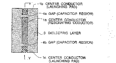
Figure 2 shows a center signal conductor pattern of the microwave
resonator fabricated in accordance with a process which will be described
- 10-
395~
hereinafter. FigLlre 2 also sllows a section taken along the line X-X in
Figure IB.
As shown in Figule 2, the center signal conductor pattern of the
microwave resonator inclucles a pair of center conductors lb and lc
aligned to each oLher but separated from each other, and another center
conductor la located between the pair of center conductors lb and lc and
aligned to the pair of center conductors lb. The center conductor la is
separated from the pair of center conductors Ib and lc by gaps 4a and 4b,
respectively. With this arrangement, the center conductor la forms an
inductor, and each of the gaps 4a and 4b -forms a co-upling capacitor, so
that a series-connected LC resonating circuit is formed. Therefore, the
center conductor la forms a resonating conductor in the microwave
resonating circuit, and each of the pair of center conductors lb and lc
forms a launching pad in the microwave resonating circuit. Specifically,
the center conductor la has a width of 0.26 mm and each of the gaps 4a
and 4b is 0.70 rnm. The launching pads lb and Ic forms a microstrip
line having a characteristics impedance of 50 Q at 10 GHz. On the other
hand7 the resonating conductor lc is in a rectangular pattern having a
width of û.26 mm and a length of 8.00 rnm.
Here, the dielectric layer 3 was formed o~ LaAlO3, and the
resonating conductor 1 a of the resonating circuit is formed of a
YBa2Cu3Oy (6<y<7) thin film. The ]aunching pads lb and lc and the
ground conductor (not shown in Figure 2) are formed of an Al
(aluminum) thin fi]m.
Referring to Figures 3A to 3D, a process of fabricating the
embodiment of the microwave resonator in accordance with the present
,:
. - 11 -
.: .
", , ~
, ~
203~5~
invenlion is illustratecl. Figules 3A to 3D show a section taken along the
line Y-Y in Figure lB and in Figure 2.
E~'irst, a LaAlO3 plate 3a having a thickness of 0.5 mm was used as
the dielectric substrate. YBa2Cu3Oy thin films were deposited on an
upper surface and an undersurface of the LaAIO3 dielectric substrate 3a
by an electron beam evaporation process. Thereafter, the oxide
superconductor thin films were patterned by a wet etching using an
etching agent of hydrochloric acid, so that a resonating conductor la is
:formed on the upper surface of the dielectric substrate 3a, and a ground
conductor 2a is formed on the undersurface of the dielectric substrate 3a,
as shown in Figure 3A.
The YBa2Cu3Oy thin films were of a thickness 6000 A. The
ground condllctor 2a h~s a width which is three times the width of the
resonating conductor la, and a length which is one and one-fifth of the
length of the center conductor la.
Thereafter, an aluminum thin film~of a thickness 6000A was -
formed on the upper surface and the undersurface of the dielectric
substrate 3a by a lift~off process, so as to ~or~ the launching pads lb and
lc and a ground conductor 2b, as shown in Figure 3B. The ground
conductor 2b was formed to completely cover the whole of the
undersurface of the dielectric substrate 3a.
Then, as shown in Figure 3C, a mask 5 was deposited on the
resonating conductor la and the launching pads lb and lc, and an LaAlO3
thin film 3b of a thickness 6000 A was grown on an uncovered portion of
the substrate 3a.
On the other hand, an LaAlO3 plate 3c having a YBa2Cu3Oy thin
film ground layer 2c and an aluminum thin film ground layer 2d folmed
.~ .
- 1 2 -
~ .
203~3S9
on an uppel surfclce thereof were prepared with the same process as that
shown in Figures 3A c~nd 3B. As shown in Figure 3D, the LaAlO3 plate
3c was closely stacked on the conductors la~ lb, and lc and the LaA103
thin film 3b of the LaAIO3 plate 3a after the mask layer 5 was removed.
Thus, the microwave resonator having substantially the same basic
structure as the sectional structure shown in Figure lB was comple~ed.
.; The resonating conductor la, the ground conductor layers 2a and
2b and the dielectric layer 3b were deposited in the following conditions
Evaporation source for YBa2Cu30y : Y, Ba, Cu (metal)
Evaporation source for LaAlO3 : La, Al (metal)
Gas pressure : 2 x 10⁻⁴ Torr
Substrate Temperature : 600 C
Film thickness of Center conductor : 6000 A
Film thickness of Dielectric layer : 6000 A
Film thickness of Ground conductor : 6000 ~
When the YBa2Cu30y thin films as mentioned above were
deposited, an O3 gas was blow onto a deposition sur~ace by a ring nozzle
located in proximity of the deposition sur:face. The blown O3 gas was
obtained by gasifying a liquefied ozone refrigerated by a liquid nitrogen.
Namely, the blown O3 gas was a pure O3 gas. This O3 gas was supplied
at a rate of 40 cm2/minute.
The microwave resonator fabricated as mentioned above was
connected to a network analyzer in order to measure a frequency
characteristics of a transmission power in a range of 2 GHz to 20 GHz.
To evaluate a frequency selectivity of a microwave resonator, it is
an ordinary practice to indicate, as Q factor, a ratio of a resonance
- frequency "fo" and a band width "B" in which the level of the
.~
13
: ~ . - . :
` :' ' :
. .
:
~0~95~3
transmission power does not drop below a leve] which is lower than a
maximum level by 3 dB. (Q = fo / B~ In addition, as a comparative
example, there was prepared a microwave resonator having the same
specification as that of the above mentioned microwave resonator in
accordance with the present invention, other than the fact that all of the
conductors are formed of aluminum. Q factor of the embodiment of the
microwave resonator of the present invention and the cornparative
example was measured. The result of the measurement is shown in the
following TABI,E.
TABLE
: . . .. __
Frequency (GHz) 4.6 9.1 13.4 17.7
... __. . _ .. . ,. ~ .
S~ Embodiment 1870 1520 1080 9~0 ~;
.. _ .
Comparative l 80 ~ . 330 450
~ s seen from the above, the present invention can give the
microwave resonator capable of operating at a liquid nitrogen
temperature ancl having a remarkclbly high Q factor, since the resonator
constituting conductor portions of a microstrip line are formed of an
oxide superconductor material layer having an excellent superconduction
characteristics.
In addition, since the conductors other than the resonator
constituting portions are formed of a normal conduction metal, the
microwave resonator in accordance with the present invention can be
.~
- 14 -
... .
' :' .` , : :
~ . .
21~95~3
connected io the existing package or parts by means of a conventional
manner.
The invention has thus been shown and described with reference to
the specific embodiments. However, it shou]d be noted that the present
invention is in no way limited to the details of the illustrated structures
but changes and modifications may be made within the scope of the
appendedclaims.
- 15-