Note : Les descriptions sont présentées dans la langue officielle dans laquelle elles ont été soumises.
Y09-89-117
20~0660
EPITAXIAL SILICON LAYER
AND METHOD TO DEPOSIT SUC~
DESCRIPTION
Technical Field
The present invention is concerned with a n-type silicon
layer which includes an n-type dopant and germanium wherein
the germanium is present in an amount that does not
necessarily result in a significant decrease in the band gap
of the layer. In addition, the present invention is
concerned with a method for epitaxially depositing an
in-situ doped n-type silicon layer onto a substrate, and is
particularly concerned with a low temperature, low pressure
chemical vapor deposition method. The present invention is
also concerned with deposited, in-situ doped n-type silicon
layers obtained by the process of the present invention.
Summary of Drawings
Figure 1 illustrates the effect of doping with phosphorous
according to prior art ultrahigh vacuum/chemical vapor
deposition reaction. Figure 2 .illustrates the effect of
employing germanium in combination with the n-type dopant
pursuant to the present invention.
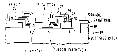
Figure 3 is a cross-sectional view of a double epitaxial,
double heterojunction PNP transistor illustrating a device
made in accordance with the present invention.
Background Art
The current desire in the electronics industry to provide
high performance integrated circuitry of reduced dimensions
has created a tendency to employ lower processing
temperatures. For instance, the dimensions of device layers
deposited by silicon epitaxy at the more typical
temperatures employed, for instance, temperatures greater
r than about 1000C, are fixed at v lues greater than the
Y09-89-117 2
`- 20~0~60
diffusion length of dopants out of the substrate onto which
the silicon is deposited. For instance, such dimensions are
typically on the order of a micron or more. However, the
production of thin epitaxial films of silicon having abrupt
and arbitrary dopant profiles is vital in device and circuit
fabrication, and particularly in applications such as
scaled-down bipolar and CMOS VLSI circuits and processes.
Various attempts at achieving lower processing temperatures
were not especially successful because of a number of
problems that need to be overcome before reduced
temperatures such as those below about 800C could be used.
For instance, at such reduced temperatures, the number of
epitaxial defects can increase markedly. Also, at such
relatively low temperatures, dopant atoms do not have
sufficient mobility to find electrically active
substitutional sites in the silicon lattice.
However, various ones of these problems have been overcome
and the ability to employ relatively low temperatures of
800C and less has been rea]ized by employing ultrahigh
vacuum as disclosed for instance by Meyerson,
"Low-Temperature Silicon Epitaxy By Ultrahigh
Vacuum/Chemical Vapor Deposition", Applied Physics Letters
48 (12), pp. 797-799, March 24, 1986, Meyerson, et al., "Low
Temperature Silicon Epitaxy By Hot Wa]l Ultrahigh Vacuum/Low
Pressure Chemical Vapor Deposition Techniques: Surface
Optimization", Journal of the Electrochemical Society, Vol.
133, No. 6, June 1986 and Srinivasan, et al., "Current
Status of Reduced Temperature Silicon Epitaxy By Chemical
Vapor Deposition", Electrochemical Society, Soft Bound
Proceeding Series, Penington, New Jersey, 1985.
In addition, a particularly effective process employing low
temperature and low pressure chemical vapor deposition of
epitaxial silicon is disclosed in the Canadian Patent
application No. 544,049 filed August 7, 1987. Although this
process is especially effective for producing quality
epitaxial silicon layers, such could still stand improvement
with respect to the amount and uniformity of the in-situ
Y09-89-117 3
2040660
n-type dopants provided. In particular, the deposition of
in-situ doped n-type epitaxial silicon films is especially
difficult at the lower processing temperatures of about
800C and less. This difficulty arises from the failure of
the n-type dopants such as phosphorous and arsenic to bond
substitutionally into the silicon lattice.
Moreover, additional complications arise from the time
varying nature of phosphorous incorporation, where the
quantity of phosphorous bound into the film in any
coordination is a strong function of deposition time. This
effect can be seen in Figure 1, where a constant flow of
phosphine into a 550C ultrahigh vacuum/chemical vapor
deposition reactor results in a continually increasing
phosphorous content in the film. Furthermore, electrical
analysis of these layers shows that the phosphorous is
electrically inactive and therefore ineffective as a
n-dopant.
Accordingly, it is a primary object of this invention to
provide an improved technique for ]ow temperature deposition
of in-situ n-doped silicon.
It is another object of this invention to provide enhanced
n-type doping in a silicon film deposited by ultrahigh
vacuum chemical vapor deposition (UHVCVD).
It is another object of this invelltion to provide an
improved low temperature technique for fabricating silicon
devices containing at least one pn junction.
It is another object of this invention to provide structures
including a silicon layer therein which are n-doped as
deposited, without the need for additional steps such as
annealing to make the dopants electrically active.
It is another object of this invention to provide improved
silicon products containing n-type doping, by the methods of
this invention.
Y09-89-117 4
2040660
It is another object of this invention to provide an UHVCVD
process that allows in-situ n-type doping of deposited
silicon films, over a wide range of doping levels.
It is still another object of this invention to provide a
method for and device having abrupt n-type doping profiles.
Summary of Invention
It has been found in accordance with the present invention
that n-type dopants can be incorporated into a silicon film
as electrically active impurities at temperatures well below
those which were previously believed necessary for such
purpose. In particular, the present invention makes the
fabrication of in-situ deposited pn and np symmetric
junctions possible, which in turn allows the fabrication of
any silicon based device. The present invention makes it
possible to control the quantity of the n-type dopant to
thereby provide dopant uniformity. Dopant uniformity is a
critical requirement for the high quality devices presently
being demanded in the electronics industry.
In particular, one aspect of the present invention is
directed to a method for depositing an in-situ doped n-type
silicon layer onto a substrate. The method includes
providing the substrate in a chemical vapor deposition
reactor zone. The temperature in the chemical vapor
deposition zone is about 800C or less and the base pressure
in the reactor zone is an ultrahigh vacuum that is less than
the partial pressures of any contaminants present in the
chemical vapor deposition zone.
A gas-containing silicon is introduced into the reaction
zone for the deposition of silicon on the substrate along
with an n-type dopant-containing gas and a germanium-
containing gas. The germanium-containing gas is present in
an amount that is effective for enhancing the in-situ
incorporation of the n-type dopant into the silicon layer as
an electronically active dopant.
-Y09-89-117 5 2040660
A further aspect of the present invention is concerned with
products obtained by the above defined process, where such products
are not obtainable with any other process at temperatures less than
750C
Furthermore, th~ present invention is concerned with a silicon
layer, preferably epitaxial, that can be included in a complete NPN
or PNP transistor, which layer includes an n-type dopant and
germanium. The germanium is present in the silicon layer in the
amount of about 1 to about 35 atomic percent.
.~
Thus, according to a first broad aspect of the present invention,
there is provided a method for depositing an in-situ doped n-type
silicon layer onto a substrate which comprises providing the
substrate in a chemical vapour deposition reaction zone wherein the
temperature in said reaction zone is about 800 C. or less and the
base pressure in said zone is in ultrahigh vacuum; and introducing
a gas containing silicon into said reaction zone for the deposition
of silicon on said substrate, and simultaneously therewith
introducing an n dopant-containing gas and a germanium-containing
gas in an amount effective for enhancing the in-situ incorporation
of said n-type dopant into said silicon layer as an electronically
active dopant, wherein the silicon layer contains 35 atomic percent
or less of Germanium.
According to a second broad aspect of the present invention, there
is provided in a chemical vapour deposition process for deposition
of in-situ n-doped silicon on a substrate at a temperature less
than 750 C. wherein the base pressure in the reaction zone where
deposition occurs is less than about 10-8 torr, the improvement
including introducing Ge into said deposited silicone during the
incorporation of a n-type dopant species into said silicon, the
amount of Ge incorporated into said silicon being sufficient to
achieve full, as deposited, electrical activation of said n-type
-Y09-89-117
5a 2 0 4 0 6 6 0
dopant species, wherein the silicon layer contains 35 atomic
percent or less of Germanium.
According to a third broad aspect of the present invention, there
is provided a method for forming a silicon bipolar transistor
having emitter, base and collector regions, said method being
characterized by the steps of:
depositing a silicon emitter layer by chemical vapour
deposition at a temperature less than`about 750C., and
in-situ doping said silicon emitter layer with a n-type dopant
species, wherein Ge is incorporated into said emitter during said
in-situ doping step in an amount sufficient to cause said n-type
dopant species to be in-situ electrically active therein, where the
silicon layer contains 35 atomic percent or less of Germanium.
Best and Various Modes for Carrying Out Invention
It has been found pursuant to the present invention that the
inclusion of relatively minor amounts of a germanium-containing gas
in the input gas in an ultrahigh vacuum/ chemical vapor deposition
UHVCVD reaction for forming an in-situ doped n-type (epitaxial)
silicon layer results in the incorporation of stable and defined
amounts of electrically active n-type dopant in the silicon film.
The surprising effect achieved by the present invention is
demonstrated by a comparison of Figure 1 with Figure 2. In
particular, Figure 1 represents prior art whereby a constant flow
of phosphine into a 550C. ultrahigh vacuum/chemical vapor
~1 deposition reactor results in a continually increasing phosphorous
content in the silicon
yo~ 9-117 6 2040660
film. Electrical analysis of these layers shows that the
phosphorous is electrically inactive.
Figure 2 and that portion of Figure 2 identified as
portion 2A substantially repeats the above process for
the first 1500 angstroms of film growth whereby the same
phenomena occurs as described for Figure 1. On the other
hand, that portion of Figure 2 identified as portion 2B
demonstrates the effect when a relatively small amount
(i.e. - about 7 atomic percent) of a germanium-containing
gas (such as germane) is included along with the
phosphine in the input gas. The results demonstrate that
the phosphorous content is increased to a stable value
where it remains. Moreover, electrical analysis of this
layer establishes that the phosphorous is fully
activated.
As is apparent from portion B of Figure 2, the onset of
n-type dopant incorporation is extremely abrupt when the
Ge-containing gas is introduced into the reaction zone.
Even though the phosphine gas has been continually
introduced, the incorporation of P as a fully
electrically active dopant species does not occur,
especially at high doping levels in excess of 1019
atoms/cc until the Ge-containing gas is introduced into
the reaction zone. At this time, the phosphorous dopant
is incorporated in the proper substitutional sites in the
silicon lattice as fully electrically active dopants.
For the low temperature (less than 750C) deposition of
silicon, gaseous sources are required which will pyrolize
at low temperatures. Typically, these will be gaseous
sources containing hydrogen, such as silane (SiH4). As a
by-product of the decomposition of the growth species, H
atoms can appear on the growth interface. Additionally,
phosphorous acts as a poison for growth in that the P can
tend to form clusters of P2 on the silicon growth
surface. When the phosphorous is present as clusters,
electrically active dopants will not be produced in the
proper sites in the silicon lattice. Also, these
YO9- ~-117 7 2040660
-
phosphorous clusters can hold H atoms on a silicon
surface, as the P-H bonds are very strong. This tends to
further inhibit both silicon growth and incorporation of
fully electrically active n-dopant species.
It is believed that the presence of Ge aids in the
desorption of H atoms from the growing surface, thereby
allowing the n-dopant to go directly to a substitutional
site in the lattice where it is fully electrically active
as a dopant. However, the presence of Ge may still be
helpful in the incorporation of n-dopant species even if
hydrogen atoms are not present on the silicon surface, by
enhancing the solubility of the n-dopant into the silicon
at low temperatures. The net effect is that the presence
of Ge increases the effective solubility of these
n-dopants into silicon.
As noted, the presence of Ge is particularly important
for low temperature n-doping of silicon, since it allows
the in-situ incorporation of fully electrically active
dopants. It also leads to an abrupt turn-on of doping
activity thereby leading to the formation of very sharp
pn junctions. The use of Ge in this manner is
particularly applicable to chemical vapor deposition
processes, but is also applicable to other processes
utilizing gaseous sources. For example, vapor phase
epitaxy using chemical vapor deposition or molecular beam
epitaxy (MBE) with gas sources are examples of processes
that can be used.
The use of a germanium-containing gas to achieve the
results obtained by the present invention was not at all
apparent from any prior art. In fact, to use germanium
as a doping enhancement in heavily doped n-type material
is contrary to prior uses of germanium whereby such is
employed in the fabrication of bipolar transistor bases
whose band gap is to be decreased. Although a reduced
band gap is desired for the base region, most heavily
doped n-type material is employed in the emitter of these
devices (NPN), where an increase in band gap is desired.
_~9-89-117 ~ 2 0 4 0 6 6 0
However, the amounts of the germanium used in the present invention
are small enough that the primary band gap reduction mechanism is the
presence of the n-type dopants at relatively high levels instead of
the effect of the germanium. Accordingly, the germanium is present in
this invention in an amount that is both effective for enhancing the
in-situ incorporation of the n-type dopant into the silicon layer as
an electronically active dopant, but less than that which would result
in a significant decrease (e.g.- a decrease more than 100 meV) in the
band gap in the device obtained. According to preferred aspects of the
present invention, in a NPN transistor, about 1 to about 35 atomic
percent of germanium is introduced in the case of a base and about 1
to about 20 atomic percent of germanium is introduced in the case of
an emitter, and most preferably about 5 to about 20 atomic percent in
the case of a base and about 2 to about 15 atomic percent in the case
of an emitter.
The germanium-containing gas employed can be any germanium gas such
as the germanium hydrides and preferably germane (i.e.- germanium
tetrahydride) Another suitable germanium-containing gas is germanium
tetrachloride.
The n-type dopants that can be employed are well known in the prior
art and need not be described herein in any great detail. However, the
preferred n-type dopants are phosphorous, arsenic, and antimony. The
phosphorous-containing gas employed can be phosphine or POCl3 or PCl3
with phosphine being most preferred due to its decomposition at low
temperatures. Suitable arsenic-containing gases include arsine or
AsCl3. A suitable antimony gas is SbH3.
The level of the n-type dopant in the silicon layer can vary over a
wide range but generally is about 1 x 10¹⁴ to about 1 x 10² atoms per
cm3. The doping level is determined based on the desired device
characteristics.
YO9 ~-117 - 9 2040660
The silicon source gas for the deposition of silicon is
not especially critical and can be any of the silicon
source gases known in the art such as silane, higher
order silanes including disilane (Si2H6), and
chlorosilanes such as SiCl4, SiH2Cl2, SiHCl3, and SiH3Cl.
It is recognized that heterojunction bipolar transistors
(HBT) have been fabricated in the art in both npn and pnp
form. In pnp HBTs, a silicon base region is used in
which Ge is present. Ge is used therein to decrease as
much as possible the band gap of the base region in order
to enhance operation of the transistors. However, those
devices are generally made in a process wherein thermal
diffusion, ion implantation or high growth temperatures
are used to place the n-dopant species and Ge in the base
region. High temperature steps, such as thermal
diffusion and high temperature annealing or high growth
temperatures are used to electrically activate the dopant
species. Thus, in prior implanted pnp HBT's, the Ge is
not introduced at the same time the n-type dopant is
introduced in the base layer, in further distinction with
the present invention where Ge and the n-dopant are
present at the same time in the reaction zone. In
deposited devices Ge and the dopant Sb are co-deposited
at high growth temperatures to activate the dopant, Sb.
The Ge used in the present invention need not be used to
significantly alter the band gap of the n-type silicon
layer, but instead to enable full electrically active
incorporation of n-type dopants in-situ. This creates
very abrupt dopant profiles, and therefore enables the
fabrication of very narrow structures.
Accordingly, in the practice of the present invention,
the product obtained by the inventive process described
herein is unique in its properties and can be used to
provide advantageous devices, such as transistors. In
bipolar transistors, it is desirable to have highly doped
emitter regions where the band gap of the emitter is not
appreciably reduced. Further, the emitter need not be
single crystalline, since the strain produced in a single
Y09-~9-117 10 2040660
crystalline material can reduce the band gap of the
emitter. By the use of this invention, n-type emitter
layers can be produced with the desired doping levels and
band gaps.
In heterojunction bipolar transistors using Si-Ge layers,
it has been the case in the prior art that high
temperatures have been required to incorporate sufficient
quantities of electrically active dopants. However, high
temperatures affect Si-Ge layers, causing them to relax
by forming defects (dislocations) which in turn adversely
affect device operation. The present invention avoids
this problem by enhancing the incorporation of fully
electrically active n-dopants at low temperatures without
leading to defect formation.
The preferred apparatus as well as process parameters for
carrying out the improved process of the present
invention are those employed in Canadian application No.
544,049. For instance, the apparatus employed is
preferably a hot wall, isothermal chemical vapor
deposition apparatus of the type shown in said Canadian
application No. 544,049. Device quality epitaxial
silicon layers can be deposited with this apparatus.
The deposition temperatures employed are about 300C to
about 800C with the preferred temperatures being about
450C to about 750C and the most preferred heing about
500C to about 550C.
The base pressure employed is less than about 10-8 Torr
and preferably less than about 1 x 10⁻⁸ Torr. The
apparatus employed is a flow system in which the source
gases (silicon source gas, n-type dopant source gas and
germanium source gas) are injected at one end and high-
speed pumps operate at the other end, there being a load
lock to eliminate contamination upon loading of the
substrates prior to deposition. The system typically
operates in a molecular flow regime where the total
operating pressure of the source gases is less then
~'09-89-117 11 2040660
several hundred m Torr during deposition. While the
preferred total operating pressure of the source gases
during deposition is about 10- to about 10-4 Torr,
source gas pressures up to several hundred millitorr may
be possible when very low growth temperatures of less
than about 500C are used.
Accordingly, the present invention enhances the
incorporation of n-type dopants into epitaxial silicon
and provides for such to be incorporated as
electronically active species without any additional
steps, such as high temperature annealing and high
temperature deposition as required in prior art
techniques.
Figure 3 is a cross-sectional illustration of a double
epitaxial double heterojunction PNP transistor in which
both the base and emitter regions are formed by low
temperature epitaxy using the aforementioned UHV/CVD
process. A two-step epitaxial process is used wherein
low temperature epitaxy i5 used to orm the base region
and another low temperature epitaxy step is used to form
the emitter region.
In the formation of the transistor of Figure 3, the base
region is hea~iily doped (phosphorus lO19cm-3) SiGe film.
Advantage is ta~en of the epitaxial base technology
because the thermal cyc]es following the base deposition,
which can ca~lse dopant diffusion and relaxation of highly
strained layers, are eliminated. As will be seen, the
insulating layers are formed by plasma enhanced CVD and
the emitter region is formed by low temperature epitaxy,
thereby limiting the temperature after base deposition to
550C and lower.
The transistor 10 is a non-self aligned structure that is
used to illustrate ]ow temperature processing technolo~y
in accordance with the present in~ention. Transistor 10
includes an extrinsic base polysilicon region 1~ and an
ion implanted collector region 14. Emitter 16 is also a
Y0 `9-117 12 2040660
low temperature epitaxial layer. A field oxide layer 18
overlies the p-type substrate 20. Plasma enhanced CVD is
used to produce oxide layers 22 and a nitride layer 24.
Reference is made to D.L. Harame, et al. IEDM, pp. 889-
890 (1988) and G.L. Patton, et al., VLSI Symposium, pp.
95-96 (1989) for discussions of a non-self aligned
structure and method. The extrinsic base polysilicon 12
is patterned and etched to form a second, smaller window
inside the opening in the field oxide 18 (the non-self
aligned opening), through which boron is implanted and
annealed to increase the collector doping concentration
in ion implanted collector 14. The intrinsic base 26 is
grown by UHV/CVD low temperature epitaxy at 550C, as
detailed by B.S. Meyerson, et al., Appl. Phys. Lett.,
Vol. 50, p. 113 (1987).
Thermal quality oxide layers 22 were deposited at 350C
using plasma enhanced CVD. An emitter opening was then
defined and etched within the non-self aligned opening
and the single crystal emitter 16 was deposited by
UHV/CVD at 550C.
As an alternative structure a NPN transistor can be made
using the same process as that used to make the
transistor of Figure 3, the only difference being that
the conductivity types are interchanged.
As a consequence of the present invention, enhanced N-
type doping is obtained, which allows wafer scale
integration to be achieved. Since the uniformity of N-
type doping concentration is extremely uniform across the
wafer, integrated circuits can be made using all NPN or
PNP devices, as well as with circuits including
complementary devices. For example, a silicon wafer
including a large number of integrated circuit chips can
be processed at one time with excellent uniformity of
device properties across the wafer. In particular,
integrated silicon heterojunction bipolar transistors can
be wafer scale integrated.
Y09 `q-117 13 2040660
The following non-limiting example is presented to
further illustrate the present invention.
EXAMPLE
An n-type epitaxial silicon layer is deposited onto a
substrate by introducing SiH4 at about 20 sccm (standard
cubic cms per minute), GeH4 at about 0.2 sccm, and 100
ppm PH3 in He at about 4 sccm at a temperature of about
550C and total growth pressure of about 1.4 m Torr. The
results obtained are illustrated in portion 2B of Figure
2. The layer illustrated in portion 2B showed an n-type
carrier density of about 4 x 10¹⁹ electrons/cm3
establishing full electrical activation of the
phosphorous dopant present.
While the invention has been shown with respect to the
embodiments described herein, it will be apparent to
those of skill in the art that variations can be made
therein without departing from the spirit and scope of
this invention. For example, the exact operating
parameters of the UHVCVD process described in the cited
co-pending applications can be varied, and the silicon
layer need not be epitaxial, although epitaxial
deposition is often preferred. While thermal CVD systems
are described in those cited co-pending applications,
other types of excitation (plasma, etc.) will be
recognized by those of skill in vapor deposition
techniques as being suitable. Further, the degree of
epitaxy is known to vary and need not be 100% lattice
matching. Still further, the use of these silicon
layers, having enhanced n-type doping, is not limited to
any particular device, but can be used in bipolar
transistors, diodes, Schottky barrier devices, FET's,
etc.