Note : Les descriptions sont présentées dans la langue officielle dans laquelle elles ont été soumises.
;?~~~~r~8
1
nttttAg~ LOW-EMISSIVITY THIN FILM INTERFERENCE FILTER
Inventor: Jesse D. Wolfe
Background of the Invention
This invention relates generally to infrared
interference filters, and more particularly, to a
durable low-emissivity filter.
The use of transparent panels in buildings,
vehicles and other structures for controlling solar
radiation is quite prevalent today. The goal of solar
l0 control is to emit light while excluding much of the
solar energy, thus decreasing the amount of air
condition or cooling required, and conserving energy.
In addition, modified glass as a structural material
provides the color flexibility architects desire.
Various processes have been employed to alter
the optical properties of these panels, including
coating glass or plastic substrates by various
techniques such as electrolysis, chemical vapor
deposition and physical vapor deposition, including
sputtering with planar magnetrons. For instance, thin
metal films have been deposited on glass or plastic to
increase the reflectance of solar radiation. Windows
deposited with a multi-layer dielectric-metal-dielectric
coating that exhibits high visible transmittance, and
high reflectivity and low emissivity in the infrared
range, are even more energy efficient. The index of
refraction of the dielectric layer is preferably 2.0 or
greater in order to minimize the visible reflectance and
enhance the visible transmittance of the window. This
dielectric layer which often consists of metal oxide
coating also offers additional protection to the fragile
~' ~~ a ~)~8
2
metal films. The optical properties of panels can also
be modified by altering the composition of the substrate
material. Nevertheless, interference filter panels
manufactured by the above-described methods have been
only partially successful in reflecting solar radiation
to the degree required for significant energy
conservation.
Another problem associated with interference
filters is their structural integrity, particularly
their inability to withstand harsh environmental
conditions. Satisfactory coatings for architectural
applications require that the coating process be capable
of producing a film of uniform composition and
thickness. Further, the process must not disturb or
otherwise degrade the substrate by overheating.
Currently, even when a uniform film is produced, it
usually must be protected from the environment. For
instance, architectural panels are often mounted so that
the coated film is on the interior surface not exposed
to the weather. Often, coated glass is sealed as part
of double glazed window unit in which the coating lies
on an inside surface where the coating is protected by
glass from abrasion and environmental materials which
could cause corrosion and degrade the optical properties
of the coating. However, when a panel is mounted such
that the reflectant film in on an inner surface, the
solar radiation must pass through the substrate twice,
first as it enters and then as it exits, thus warming
the substrate even more than a single pass.
Current transparent panels having high
reflectivity for solar radiation are unsatisfactory in
that the panels are subject to chemical and mechanical
degradation and reflect color of visible light over a
wide band.
Therefore, it is a primary object of the
present invention to provide a durable, thin-film
20~~~.~~8
3
interference filter which transmits visible light while
reflecting infrared radiation, thus having a low
emissivity value.
It is another object of the present invention
to provide an interference filter which gives less
reflected color of visible light over a wide band.
~ummarv of the Invention
These and additional objects are accomplished
by the present invention, which provides a durable,
thin-film interference filter which comprises a
substrate onto which is deposited a dielectric layer,
followed by one or more successive layers of metal and
dielectric layers. In between the dielectric and metal
layers is deposited a "nucleation" or glue layer that
promotes adhesion between the dielectric to the metal.
In one preferred embodiment of the invention, the
interference filter comprises a glass substrate onto
which is deposited a thin-film design consisting of five
layers, namely: silicon nitride, nickel-chromium alloy,
silver, nickel-chromium alloy, and silicon nitride.
In this preferred embodiment, the interference
filter offers excellent solar control. In addition, the
durability of the film obviates the need for a thick
protective glass covering. Indeed, the filter when
coated on panels can be utilized with the film exposed
to the exterior of buildings. Finally, by changing the
materials and thicknesses of the layers in the film it
is possible to vary the optical and electrical
characteristics of the filter.
Additional objects, advantages and features of
the present invention will become apparent from the
following detailed exemplary description, which
description should be taken in conjunction with the
accompanying drawings.
4
brief Description of the Drawings
Figure 1 is a cross-sectional view of a three-
layer design thin-film interference filter produced in
accordance with this invention.
Figure 2 is a cross-sectional view of a five-
layer design thin-film interference filter produced in
accordance with this invention.
Figure 3 is a cross-sectional view of a nine
layer film design thin-film interference filter produced
in accordance with this invention.
Figure 4 is a graph illustrating the spectral
transmittance and reflectance of a thin-film
interference filter.
pescription of the Preferred Embodiments
A thin-film interference filter incorporating
the present invention is shown in Figure 1. As shown
therein, the filter consists of a transparent substrate
2 which is provided with two planar parallel surfaces 4
and 6, in which surface 4 is exposed to the medium and
surface 6 is coated. The substrate can be formed of any
suitable transparent material; however, the substrate is
preferably a material which has superior structural
properties and minimum absorption in the visible and
near-infrared spectra regions where the solar energy is
concentrated. Crystalline quartz, fused silica, soda-
lime silicate glass, and plastics such as polycarbonates
and acrylates, are all preferred substrate materials.
Deposited onto the substrate surface 6 is a
dielectric layer 8 followed by a metal precoat layer 10.
In this embodiment, silicon nitride has been found to be
a particularly satisfactory dielectric material. other
dielectric materials which can also be utilized include
titanium oxide, silicon oxide, zirconium oxide, and tin
oxide. The thickness of the dielectric layer ranges
y~c~
from approximately 300 to 900 angstroms, and more
preferably from approximately 400 to 600 A.
Precoat layer 10 is preferably maintained as
thin as possible so that it will have very little, if
5 any, adverse effect upon the optical characteristics of
the substrate or the subsequent metal layer. Precoat
layers with thicknesses ranging from approximately 5 to
20 A have been satisfactory: more preferably, the
thickness is between approximately 8 to 12 A. This thin
precoat layer can be formed from any number of
materials. It has been found that nickel-chromium alloy
comprising approximately 1 to 80 percent nickel and
approximately 1 to 20 percent chromium can be used as a
precoat; more preferably, the alloy content is
l5 approximately 80 percent nickel and 20 percent chromium.
Other metals and alloys thereof that can be used as a
precoat include nickel, chromium, rhodium, and platinum.
The precoat layer apparently acts as a glue or
"nucleation" layer. It is believed that while the
precoat layer is thin enough not to adversely affect the
optical properties of the filter, it causes the metal
film to behave as if it were a homogeneous metal slab.
Finally, a metal layer 12 is deposited onto
the precoat layer. The metal layer can be formed from
a number of materials, with silver being particularly
satisfactory. Other metals which also can be utilized
are gold, copper and platinum. The thickness of the
metal layer ranges from approximately 40 to 15o A, and
more preferably, from approximately 55 to 85 A. In the
embodiment as illustrated in Figure 1, the metal layer
is exposed to medium and therefore the film should be
positioned toward the interior environment.
To increase durability, an additional
dielectric layer can be deposited. As shown in Figure
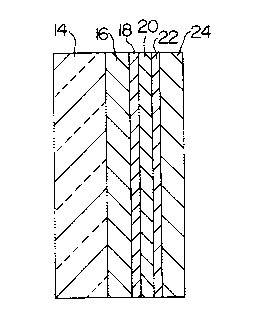
2, in this preferred embodiment, transparent substrate
14 is first coated with a dielectric layer 16, that is
1
6
then followed with a precoat layer 18, and thereafter
with a metal layer 20. As is apparent, the description
thus far coincides with the embodiment as described in
Figure 1. However, a second precoat layer 22 is
deposited onto the metal layer and thereafter a final
dielectric layer 24 is deposited over the second precoat
layer. This second precoat layer can be formed from the
same material and in the same thickness range as precoat
layer 10 in Figure 1. Similarly, the final dielectric
layer can be formed of the same material, and of
approximately the same thickness as the dielectric layer
described in Figure 1, though the preferred thickness
range is between approximately 575 to 860 A. As will be
described in greater detail below, this preferred
embodiment offers better mechanical and corrosion
resistance.
In another preferred embodiment of the
invention as shown in Figure 3, the interference filter
consists of a transparent substrate that is coated with
a nine-layer film. The first five layers deposited onto
substrate 26 are identical to those identified in Figure
2, namely: a dielectric layer 28, a precoat layer 30, a
metal layer 32, a second precoat layer 34, and lastly,
a second dielectric layer 36. These five layers are
formed from the same materials and of the same
comparable thicknesses described previously for Figure
2. However, in this embodiment, following dielectric
layer 36 are four additional layers consisting of first
a third precoat layer 38, a second metal layer 40, a
fourth precoat layer 42, and finally, a third dielectric
layer 44. The third and fourth precoat layers can be
formed of the same materials and of the same thicknesses
as the precoat layers described in Figures 1 and 2.
Similarly, the metal layer can be formed of the same
material and of the same thickness as the previously
described metal layers for Figures 1 and 2. Finally,
r'i ;,1 ,. ~ '
ls' v ~.i-. _~~ ~ PJ
7
the dielectric layer can be formed of the same material
and of the same thickness as previously described
dielectric layers.
Aside from increasing the overall durability
of the interference filter, increasing the number of
layers also has the effect of increasing the.
electromagnetic optical interference and electric
conductivity of the filter.
In addition, variations on the materials and
thicknesses for each layer in each of the above
described embodiments can vary the optical and
electrical characteristics of the filter. Indeed, by
such variations, the light transmission can range from
10 to 80 percent of visible light. Moreover, solar
rejection can range from 0 to 50 percent, and finally,
the electrical sheet resistance can range from 3.0 to 30
ohm per square. The filters described in Figures 2 and
3 can be referred to as "monolithic" because there is no
need for a thick protective glass cover. In these
embodiments, the dielectric layers serve to protect the
soft metal layers against chemical and mechanical
degradation.
The films described above are prepared by DC
reactive sputtering with a rotating cylindrical
magnetron. The magnetron reactive sputtering technique
is particularly useful for depositing dielectric films.
While there are other techniques for depositing the
metal and dielectric layers such as thermal oxidation
and LPCVD (low pressure chemical vapor deposition),
these methods suffer from, among other things, slow
deposition rates. Moreover, RF planar magnetron
sputtering for depositing dielectric material is
impractical for large-scale industrial applications
because of the enormous power requirements; however,
planar magnetrons can be used to deposit the metal and
precoat layers. Finally, conventional "wet, dip and
CA 02041038 2000-06-27
8
dry" methods for large-scale operations are inadequate
for applications requiring high purity and precise,
uniform film thicknesses. Moreover, with sputtering, no
heating of the substrate is required.
A description of the method for coating
substrates with dielectric materials such as silicon
dioxide and silicon nitride is found in US Patent No.
5,047,131 issued September 1991.
IO
Experimental Results
Durable low-emissivity interference films of
the invention were originally deposited by a research
size in-line cylindrical magnetron manufactured by Airco
Coating Technology, a division of Assignee. The same
results were later duplicated in a larger cylindrical
magnetron, the C-MagT~ model 3000 cathode, also
manufactured by Airco under substantially the same
process conditions. In addition, more sophisticated
applications of the inventive method are possible with
the model 3000. The research coater is capable of
substrate sizes up to 16 inches wide, whereas the larger
coater is capable of substrate sizes up to I meter wide.
Research coaters normally operate at approximately 3 kw
power whereas the model 3000 normally operates between
to 40 kw. Tests indicate that the research and model
3000 produce film of the same quality. Both systems use
untrapped diffusion pumps that achieved a base pressure
in the 106 Torr range before operation. Argon was used
30 as an inert gas and nitrogen was used as the reactant
gas when depositing silicon nitride. The partial
pressure of the gas was determined by the transition
from the nitride mode to the metallic mode. Experiments
were run as close to that transition as practicable.
n.rr ly .~
f.:L~:~_~b~F~
9
The pressure and flow rate of the sputtering gases were
controlled by conventional devices.
The power applied varied for the different
target materials but for the most part it was comparable
to the maximum obtainable with similar size planar
magnetrons. Each sputtering source was connected to an
appropriate direct current power source having provision
for automatically maintaining the voltage, current or
power, as desired.
l0 Because the electrical conductivity of pure
silicon is so low that it is unsuitable for sputtering
with direct current, the silicon target was impregnated
or doped with a small amount of aluminum in the range of
from 2-4%. The target was prepared by plasma spray.
With nitrogen as the sputtering gas, the
coating contained a mixture of aluminum and silicon
nitrides. All of these components are relatively hard
and form an amorphous film that acts as a strong
barrier. However, the amount of aluminum in the film
did not interfere with formation of the desired silicon
based compound films. In the course of the experiments,
films were sent out for independent RBS (Rutherford
Back-Scattering) sampling to determine the composition
of the compound. The silicon nitride measured 42%
Si/57% N, which is very close to the theoretical 3:4
ratio for nitride (Si3N4) .
The target was conditioned using an inert gas,
then the process gas was added until the desired partial
pressure was reached. The process was operated at that
point until the process was stabilized. The substrates
were then introduced to the coat zone and the film was
applied. The substrate used was typically soda lime
glass.
Tables 1 and 2 set forth the process data for
deposition of films as described in Figure 2.
to
TABLE 1
Thickness SCCt! SCCM Potential Power Current Pressure No. Substrate Speed
a er fA) lr Np_cy) ctu)cA) cu) ses cin/min)
Si3N4 490 12 60 452 4.08.68 2.061 30.8
NiCr 8 40 Na 427 0.3.58 2.061 187.9
Ag 75 40 Na 430 0.51.05 1.371 168.0
NiCr 8 40 n/a389 0.15.30 2.061 187.9
Si3N4 720 12 60 458 4.08.69 2.041 30.0
The above filter had the following optical and
electrical characteristics:
% Transmittance (integrated D65 source) 75.96
% Reflectance of the film covered side 5.96
% Absorbance 16.30
Electrical sheet resistance 14.7-15.3
TABLE
2
ThicknessSCCHSCChPotentialPoser PressureNo. Substrate
Current Speed
a er cA) I~rW2_cV) cku> (A) (u) a lin/min)
ses
Si3N4 491 12 60 600-9604.0 8.70 1.85 1 23.1
NiCr 10 30 n/a361 0.2 .44 1.00 1 142.4
2 0 Ag 70 40 n/a509 1.3 2.64 1.40 1 197.2
NiCr 10 30 n/a361 0.2 0.31 1.02 1 142.4
Si3N4 715 12 60 600-9404.0 8.75 1.92 1 15.9
The above filter had the following optical and
electrical characteristics:
% Transmittance (integrated D65 source) 73.57 '
% Reflectance of the film covered side 4.70
% Absorbance 20.00
Electrical sheet resistance 17.7-18.8
Curve 50 (Rf) in Figure 4 illustrates the
reflectance of the interference filter produced under
the parameters set forth in Table 2 as measured from the
film side. Curve 52 (Rg) is the reflectance of the
uncoated substrate side and curve 54 (T) is the
transmittance.
C5 v .n
... ~.~ m
11
A comparison of the durability of the
inventive filter to prior art filters was made. The
inventive filter tested consisted of a substrate coated
with a five layer film as illustrated in Figure 2. For
convenience, the inventive film design structure is
designated as:
G1 ass/ S i3N,~/N i Cr/Ag/Ni Cr/S i3N4
Similarly, the names and design structures of the four
prior art filters are:
Standard Low-E Glass/Zn02/Ag/Zn/ZnOZ
Super-E II Neutral Glass/Zn02/Ag/Zn/ZnOZ/TiOZ/Zn02
Phase I Glass/Zn02/A1z03/Ag/Al/A1203/Zn02
Phase II Glass/SiOz/Zn02/Ag/Zn/Zn02/SiOz
The procedures of the tests that were
performed on these filters are described herein and a
tabulation of the results follows thereafter.
Abrasion Resistance: The durability of the filters was
measured with a Taber Abrader. A CS10F wheel with 500
gram weights was used. For the standard Taber score the
sample was rotated under the wheels for 50 revolutions.
The area of the abrade was observed through a microscope
at 50 times magnification and a picture was taken. Four
1" x 1" squares were drawn on the picture in random
places and the number of scratches inside these squares
was counted. The number of scratches in all four
squares was averaged and the part was given a Taber
score based on the following formula:
TABER SCORE = # SCRATCHES * (-0.18) + 10
The Taber score is a linear scale where no scratches is
a 10, and 50 scratches is a 0. For reference, uncoated
soda lime glass typically scores about 9Ø
~" ~~
12
72 Hour Hiah Temperature Humidity
Duration: 72 hours
Temperature: 92C
RH: 98%
24 Hour (Mil Spec , Humidity
Duration: 24 hours
Temperature: 50C
RH: 98%
~4 Hour Salt FQg
Duration: 24 hours
Temperature : 50C
20% NaCl addition to water supply
steam Test
Duration: 10 minutes
Temperature: Water brought and tained a boil
main at
Eraser Test
Mil. Spec. erasure rubbed forciblytimes
(one stroke = 1 rub)
Fingerprint Simulation
20 Samples were exposed to a solution oil and
of lanolin
NaCl. The samples were assigned based on
a score (0-10)
the damage, a 0 being total damage.
Results
Standard Inventive
Low-E Super-E II hase I hase Filter
I
Steam Fail -- Pass Pass Pass
Erasure Fail Fail Fail 100 Pass500 Pass
Taber Fail Fail 20 Pass 50 Pass 50 Pass
Score 0 0 0 9.0 9.1-9.5
3 72-Hr. Fail -- Fail Fail Pass
0
Humidity
24-Hr. Fail Pass -- Pass Pass .
Humidity
24-Hr. Fail Fail Fail Fail Pass
Sal t Fog
Lanolin Fail -- -- Fail Pass
Score 0 0.5 9.5
13
Although the invention has been described with
respect to its preferred embodiments, it will be
understood that the invention is to be protected within
the full scope of the appended claims.