Note : Les descriptions sont présentées dans la langue officielle dans laquelle elles ont été soumises.
204216~
PROCESS FOR PRODUCING ANODIC FILMS EXHIBITING COLOURED
ATTERNS AND STRUCTURES INCORPORATING SUCH FI~MS
BACKGROUND OF THE INVENTION
I. FIFLD OF THE INVENTION
This invention relates to the formation of anodic films
having areas of discernably different colours, shades, hues or
colour densities forming patterns, printing or other indicia
(referred to hereinafter generally as coloured patterns) and
to structures incorporating such films.
II. DESCRIPTION OF THE PRIOR ART
Anodizing is a well known surface treatment carried out
on articles made of (or coated with) aluminum or anodizable
aluminum alloys for the purpose of improving the decorative
appeal of the articles and/or for improving surface
durability. The procedure involves electrolysis carried out
in an electrolyte containing a strong acid, such as sulphuric
acid, phosphoric acid, oxalic acid or the like, using the
aluminum article as an anode. As the electrolysis proceeds,
an anodic film of aluminum oxide grows on the metal surface,
with the thickness of the film increasing as the electrolysis
continues. Competition between the growth of the anodic film
and dissolution of the oxide by the acidic electrolyte creates
a film having pores which extend from the external film
surface inwardly towards the metal article. However, the
innermost ends of the pores are always separated from the
metal surface by a very thin barrier layer of dense
imperforate anodic oxide. If a non-porous anodic film is
desired, the anodization can be carried out in a less acidlc
electrolyte, but only very thin films can be produced in this
way depending on the voltage used for the anodization
procedure, so the formation of porous films is more usual.
Articles anodized in this way have surfaces which range
from grey (i.e. the colour of the underlying metal, generally
referred to hereinafter as "colourless" or "clear") to white
in appearance depending on the thickness of the oxide film,
but various procedures have been developed to colour the
anodic films in order to improve the appeal of the articles to
the eye. These range from the so-called ANOLO~ (trade mark of
16~
ALC~N ALUMI ~L~ LTD) pr~cesses, which involve the electrolytic
deposition of a metal (inorganic pigment) into the pores, to
the use of dies or organic pigments to cause staining of the
anodic film.
While these colouring procedures have been applied
successfully for many purposes, they suffer from certain
disadvantages. For example, articles coloured by the ANOLOK
procedures (as disclosed in our prior US patents ~,066,816 of
January 3, 1978 and ~,310,586 or January 12, 1982, both to
Sheasby et. al.) may exhibit lack of colour uniformity and the
procedure may be difficult to control. Articles coloured by
organic pigments and the like exhibit fading when exposed to
W light, and have therefore not been used extensively in
exterior (e.g. architectural or automotive) applications.
Moreover, when it is desired to produce coloured patterns
on the surfaces of anodized articles, resort has generally
been made to the use of adhering masks and the like to cover
certain areas of the surface while other areas are subjected
to a colouring treatment. The masks then have to be removed
and, if desired, further areas masked so that the uncoloured
areas can themselves be coloured. This is not only a complex
and expensive procedure, it also requires the use of masking
materials and solvents that may cause environmental problems
when disposed of.
2S In our prior US patent application Serial No. 07/497,222
filed on March 22, 1990, a method is described of producing
optical interference structures incorporating porous anodic
films in which interference colours are generated by the
inclusion of semi-refective layers into the films by
electrodeposition and the like. It is disclosed that the
deposits may be made more resistant to leaching by replacing
the deposited metal with a noble metal which is much more
corrosion resistant. However, the method is used only for
producing films of uniform colour throughout, rather than
patterned films. If patterns are required, masking techniques
must again be employed.
ZO4~1~3:
OBJECTS OF THE INV~NTION
It is therefore an object of the invention to provide a
process ~hich can result in the production of patterned anodic
films which are less susceptible to colour loss (fading) or
loss of colour uniformity, while providing a good range of
colours.
It is also an object, at least of preferred forms of the
invention, to provide a process which can produce coloured
patterns on anodized surfaces without resort to the use of
masks temporarily adhered to the anodized surfaces.
Yet another o~ject of the invention is to provide a
process for producing coloured patterns on an anodized surface
by a procedure which generates colours at least partially by
interference effects.
SUMMARY OF T~E INVENTION
According to one aspect of the present invention there is
provided a process for producing a structure incorporating an
anodic film exhibiting a coloured pattern, which process
comprises anodizing a surface of a substrate made of or coated
with an anodizable metal selected from the group consisting of
aluminum and anodizable aluminum alloys, to produce an anodic
film preferably having pores therein formed on an underlying
metal surface; depositing a semi-refective layer of a non-
noble metal on or within said film such that reflections from
said semi-refective layer contribute to the generation of a
visible colour by effects including light interference; and
contacting limited areas of said film with a solution of a
noble metal compound by a maskless techni~ue in order to at
least partially replace said non-noble metal in said limited
areas with said noble metal while leaving said non-noble metal
in other areas of said film unarfected.
According to another aspect of the invention there is
provided a structure incorporating a patterned anodic film,
said structure comprising a metal substrate; an anodic film
overlying said substrate; and a semi-refective layer on or
within said film, in limited areas thereof, comprising
deposits of a noble metal, said semi-refective layer
Z04L~
contributing to the generation of a visible colour by effects
including light interrerence; said film including areas other
than said limited areas exhibiting a colour different from
said colour of said li~ited areas.
According to yet another aspect of the invention, there
is provided a thin flexible membrane having a coloured
pattern, comprising a thin flexible metal substrate;
an anodic film overlying said suostrate, a semi-refective
layer on or within said film, in limited areas thereof,
comprising deposits of a noble metal, said se~i-refective
layer contributing to the generation of a colour by effects
including light interference; said film including areas other
than said limited areas exhibiting a colour different from
said colour of said limited areas; and a layer of transparent
lS flexible material overlying and supporting said anodic film.
It should be appreciated that, throughout this disclosure
and the accompanying claims, when reference is made to
different colours, it is intended that this expression should
include any discernable differences whatsoever of the coloured
areas, including differences of colour shade, hue or
saturation of a single colour as well as distinctly different
colours. It should also be appreciated that the term
"pattern" or any derivative thereof is intended to include any
abstract, irregular or regular pattern, printing, marking,
indicia or any other shape or arrangement of areas of the
anodic film having different appearance.
Furthermore, by the expression "maskless techniques" we
mean techniques of applying the solution of the noble metal to
the anodic film which avoid the prior application of adhering
masks to the anodic film. Examples of such maskless
techniques include flexographic printing of the noble metal
solution onto the anodic film, rubber stamping, spraying
coarse droplets, pulsed spraying to form random dot or streak
patterns, application by pen, paint brush or sponge, spraying
through a stencil, silk screening, etc.
BRIFF DESCRIPTION OF THE DRAWINGS
Figs. l(A) to (E) show cross-sections of an aluminum
article at the surface region thereof after various steps in a
preferred baslc process according to the present invention;
Fig. 2 is a cross-section similar to those in Fig. 1
af.er a first optional additional step;
S Fig. 3 is a cross-section similar to those in Fig. 1
after a second optional additional step;
Fig. 4 is a c-oss-section similar to Fig. 3 following a
final voltage reduction step during anodization to make the
anodic film detachable from the metal article;
Fig 5. shows the film of Fig. 4 detached from the metal
article and provided with a thin layer of reflective metal;
and
Fig. 6 is a cross-section of a patterned structure formed
by the process of the invention, in which the metal is
deposited on top of the anodic film rather than in the pores
of the film.
Like elements are identified by like reference numerals
throughout the various figures.
It should be noted that the various elements of any
particular figure are not drawn to scale.
DETAILED DESCRIPTION OF THE PREFERRED EMBODIMENTS
Figs. l(A)-l(E) show the steps of a basic preferred
process according to the invention. Fig. l(A) shows an
article 10 made of, or coated with, aluminum or an anodizable
aluminum alloy acting as a substrate for the formation of an
anodic film and having an outer surface 12. The article may
be, for example, a thin flexible foil, a laminate, a plate, a
sheet, an extrusion, a casting, a shaped element or any other
article of manufacture of the kind normally subjected to
anodization either for decorative reasons (e.g. as a
decorative article or packaging) or for protection (e.g. for
use in architectural or automotive applications).
As shown in Fig. l(B), in the basic procedure, the
article 10 is first subjected to a porous anodization step to
form an anodic film 11 on an underlying outer surface 12 of
the article, the film having pores 14 extending inwardly from
the outer surface 15 of the film towards the metal article 10.
2~4~6~
The for~ation of the porous anodic film can ~e achieved
in the conventicnal manner, e.g. by immersing the surface 12
in an electrolyte containing an incrganic acid, such as
sulphuric acid, phosphoric acid or chromic acid, or an organic
acid such as oxalic acid, or a mixtures of such acids,
providing an electrode in contact with the electrolyte and
applying a voltage between the electrode and the article.
The voltage may be AC, DC, AC/DC, high voltage, low voltage,
ramped voltage, etc. and is normally in the range cf 5-110 V.
However, the final stage of the anodization should be carried
out in such a way that inner ends 16 of the pores 14 remain
se~arated from the metal article 10 by a thin barrier layer 1
of imperforate anodic oxide of suitable thickness to permit
subsequent electrolytic deposition of a metal in the pores 14.
The barrier layer 17 should consequently have a thickness in
the range of 20-sooA~ and more preferably 50-200A. This can
be achieved by carrying out at least the last few seconds of
the anodization under DC conditions with the article 10
forming the anode at a voltage of between 2-50 volts,
preferably 5-20 volts.
While the pores 14 may be of uniform thickness through-
out their length as shown in Fig. l(B), it is more preferable
to produce pores having narrow outer portions and wider inner
portions (not shown). This results in metal deposits in the
wider portions having larger outer surfaces, which in turn
leads to stronger reflections from these surfaces and thus to
enhanced interference effects and stronger generated colours.
So-called "bottle neck" pores of this kind can be produced by
changing the acid of the electrolyte part of the way through
the electrolysis procedure from a less corrosive acid (e.g.
sulphuric acid) to a more corrosive acid (e.g. phosphoric
acid) (for more details of this procedure, see our US Patent
4,066,816 to Sheasby et al, the disclosure of which is
incorporated herein by reference).
The film 11 can be made to have virtually any desired
thickness by carrying out the electrolysis for a suitable
length of time. For decorative interior applications, the
204~
film ll may be just a fe-~ microns thick, but for architectural
or automotive applications, the film may be up to 25 microns
or more in thickness.
Metal deposits 18 as shown in Fig. l(C) are then
introduced into the pores 14 at their inner ends by an
electrodeposition technique. This can be achieved, for
instance, by the procedure descri~ed in our US Patent
4,066,816 mentioned above. For example, the anodized surface
may be immersed in an acidic solution of an appropriate metal
salt (e.g. a salt of nickel, cobalt, tin, copper, silver,
alloys such as Sn-Ni and Cu-Ni, cadmium, iron, lead, manganese
and molybdenum) as an electrolyte, a counter electrode (made
for example of graphite or stainless steel, or nickel, tin or
copper when the electrolyte contains a salt of the
corresponding metal) provided in contact with the solution and
an alternating voltage applied between the article and the
counter electrode.
As will be seen from Fig. l (C), the electrodeposition is
not usually continued until the pores 14 are completely filled
but rather until the outer ends 19 of the deposits 18
collectively form a semi-refective surface which is separated
from the underlying metal surface 12 (the oxide/metal
interface) by a distance in the order of 500-3000A (0.05 - 0.3
microns). Optical interference can then take place between
light reflected from the surfaces 19 of the deposits 18 and
the surface 12 of the underlying metal. This results in the
production of an interference colour whose appearance depends
largely on the difference in optical path of the light
reflected from the two surfaces but also partly on the light
absorption properties of the deposits 18. Since the present
inventiGn relies on the generation of colour to a large extent
by interference effects, only small amounts of the metal need
be deposited, so short term and/or low voltage deposition is
generally used. The result is a range of attractive colours,
including blue-grey, yellow-green, orange and purple,
depending on the identity of the electrodeposited metal and
the height of the deposits.
204;~1Ç;~l
Follo~ing the introduction of deposits 18 into the pores,
limited areas of the surface 15 of the anodic film 11 are
contacted by a maskless technique with a solution 20
containing a dissolved salt of a noble metal, e.g. platinum,
palladium, gold etc., with the preferred noble metal being
palladium, in concentrations ranging from 0.05 to 100 g/1,
preferably 0.2 to 10 g/1. The original deposits 18 in the
pores contacted by the solution 20 act as seeds for deposition
of the noble metal and are at least partially replaced by the
noble metal in the solution. Consequently, as shown in Fig.
l(E) by the differences in shading, deposits 21 in the treated
areas differ from the deposits 18 in the untreated areas.
These differences lead to differences in light absorption
which in turn lead to difference in the observed colours of
the treated and untreated areas. At present, the greatest
colour contrast has been obtained when using silver for
deposits 18 and Pd salts in the noble metal contacting
solution. Colour changes from yellow to violet can then be
produced when the noble metal solution is applied.
Since very little of the solution 20 is required, and
since there is no requirement to contact the solution with
electrodes or the like, the solution 20 can be applied without
the need for prior application of an adhering mask to the
surface 15, although a non-adhering mask, such as a stencil or
silk screen, could be used to limit the areas of contact
between the surface 15 and the solution 20 applied, for
example, by spraying, brushing or wiping. Even such a non-
adhering mask may not be required, however, if the solution is
applied by a technique which restricts the area of
application, e.g. flexographic printing, rubber stamping,
painting, flowing, wiping, coarse spraying (to form separated
droplets on the surface 15) or pulsed spraying. The solution
20 is usually applied in such small quantities that drying
takes place very rapidly so smearing of the pattern can be
avoided. Moreover, when the solution contains a low
concentration of the noble metal, most of the noble metal is
rapidly precipitated onto the contacted deposits and exhausted
9 204~16~.
from the solution, so subsequent rinsing (e.g. -.Jith deionized
~ater) does not smear the pattern.
The article bearing the resulting pattern of contrasting
colours can ~e used if desired without further treatment steps
and the colours thus obtained include dark brown on bronze,
grey on brown, brown on grey or yellow, etc. However, the
normal pore-sealing steps usually carried out after anodizing
treatments, e.g. immersion in near-boiling water at or about
neutral pH, can be employed and/or the surface 15 may be
covered by a protective transparent film (not shown) attached
by means of an adhesive or by heat sealing. Such a film would
normally be a polymer sheet made, for example, of polyester.
The noble metal deposits 21 are stable and thus do not
undergo fading or loss of colour uniformity. The remaining
deposits 18 are as permanent as the deposits in conventional
ANOLOK treatments and thus leaching may take place during
subsequent processing steps. The deposits 18 can be made more
resistant to leaching by a final rinse with a chromate
solution prior to any pore sealing or laminating step.
If desired, additional visual effects can be imparted to
the patterned articles produced by the basic procedure
described above by carrying out a pretreatment of the surface
of the metal article 10. For example, caustic etching may be
employed to impart a satin finish, mechanical or chemical
polishing may be used to create a bright finish, or
sandblasting can be carried out for a dull finish, etc.
Although the steps shown in Fig. 1, referred to as a
preferred basic process, are capable in themselves of
producing an attractively patterned article, further steps and
processes can be carried out, if desired, in order to create
additional colours, appearances and colour combinations.
For example, structures having coloured areas on a
colourless or white bac~ground can be produced by removing the
non-noble deposits 18 from the pores 14 prior to any pore
sealing, dichromate treatment or lamination of the structure
of Fig. l(E). The deposits 18 can be removed, for example, by
exposing the porous film to an oxidizing and/or an acidic
~U4~-~ ~
solution which leaches out the deposits 18 while leaving the
noble metal deposits 21 substantially unaffected. Such a
leaching step is not difficult because the deposits 1~3 are not
usually very voluminous in vie-~ of the fact that light
interference effects are relied on extensively for the colour
generation. Moreover, if this step is intended, the metal
selected for the deposits is preferably one having low
resistance to leaching, e.g. cobalt.
Acidic aqueous solutions can be used for the leaching
step and the structure can either be immersed in the solution
or the solution can be sprayed onto or poured over the film
11. A 5~ nitric acid solution requires only 1 to 5 minutes to
leach out the non-noble deposits. Other acids, oxidants, etc.
can be used provided the anodic oxide film is not thereby
damaged beyond usefulness.
The resulting film is as shown in Fig. 2, in which the
areas of the film 11 having empty pores 14 are colourless and
the limited areas having the deposits 21 appear coloured. The
colours which can be generated in the limited areas are
basically as described in our prior US Patent No. 4,068,816
(particularly Examples 4 and 5).
It is also possible to produce structures having a
further range of colours against a colourless bac~ground by
carrying out a further anodization step on the structure of
Fig. l(E) prior to any sealing, laminating or dichromate
treatment. Such a step is similar to the process disclosed in
our prior US patent 4,310,586 to Sheasby et. al. (the
disclosure of which is incorporated herein by reference). The
electrolyte used for the further anodization step, which may
be one of those mentioned above for the initial anodization
step, at least partially leaches the non-noble metal deposits
18 out of the pores 14 while leaving the noble metal deposits
21 unaffected so the overall result is similar to the simple
treatment mentioned above. However, the additional
anodization step thic~ens the film 11 and increases the
separation of the remaining deposits 21 from the underlying
metal surface 12. This changes the interference effects
-- 2(142,16~
generated by reflections from the semi-refective surface
formed by the deposits 21 and the surface 12. The voltage
employed for the additional anodization must be sufficient to
overcome the electrical resistance imposed by the existing
barrier layer 17 and metal deposits 18, 21. In general, the
voltage should be eoual to or greater than the final voltage
used for the for~ation of the structure of Fig. l(B).
The resulting film has the structure shown in Fig. 3.
The increase in film thickness below the deposits 21 (compare
distances "x" and "y" in Figs. 2 and 3, respectively) results
in the generation of additional interference colours for the
reason mentioned above. For such interference colours to be
produced, the additional layer of film ll grown beneath the
deposits 21 should be kept below 1 mlcron, preferably 0.05 -
0.75 microns. The colours which can be obtained in this way
are clear blues, reds, greens, purples, oranges, etc. free of
"muddiness" or bronze colours often associated with
electrodeposited metals.
Further processes can be carried out, if desired, in
order to produce structures having coloured areas on a
coloured background. While this is true of the structure of
Fig. l(e), the structure can be modified to increase the range
of colours of both the patterned and background areas. This
can be achieved in several ways, as indicated in the
following.
First of all, the non-noble metal deposits 18 may be only
partially leached from the pores 14 during a subsequent
leaching step or a subsequent anodization step of the type
mentioned above. Partial leaching of the deposits 18 can be
achieved either by using a non-noble metal which is moderately
resistant to leaching, e.g. Sn-Ni and Cu-Ni alloys, or by
using an acid in the leaching solution or electrolyte that is
less aggressive than the acids used for complete removal of
the deposits. The resulting structures often exhibit a
coloured pattern on a background of the same, but less
saturated, colour. The structures are similar to those of
Figs. 2 and 3, but the empty pores 14 shown in these figures
204~
contain deposits of reduced volume.
In a further modification of the process, the structure
of Fig. l(E) may be made to undergo further anodization, as in
the process leading to the structure of Fig. 3, but the
further anodization may be interrupted prior to complete
removal of the non-noble metal deposits 18 from the pores 14
and the entire film 11 may then be contacted with a solution
of a noble metal salt in order to replace (at least partially)
the partially leached deposits 18 with a noble metal. The
further anodization step may then be continued without further
loss of the partially leached deposits, thus maintaining the
colour saturation of the background while enabling additional
colours to be generated in the patterned and background areas
by the production of a thickened film 11. This has the
advantage of enabling a greater range of colours to be
produced both in the patterned and background areas without
employing a highly acid resistant metal to form the initial
deposits 18.
Finally, a structure having a pattern of one colour on a
background of the same colour of different saturation can be
produced merely by contacting the entire surface of the
structure of Fig. l(E) with a dilute solution of a noble metal
salt. This at least partially converts the remaining deposits
18 to noble metal, thus making them resistant to leaching,
while maintaining a difference in colour saturation between
the patterned areas and the background.
The procedures described above have all been concerned
with the production of a patterned anodized surface on an
article (substrate) made of or coated with aluminum or an
aluminum alloy. The process of the invention can, however, be
used to form a patterned anodic film structure detached from
the aluminum-containing article on which it was formed. The
present invention includes the formation of such detached
patterned films which can be produced in the manner indicated
below.
Any one of the structures referred to above, e.g. the
structures of Fig. l(E), Fig. 2, Fig. 3 or the partially
,, ' ,
- - . . ~ .
20~ 6~
leached structures, may be made to undergo a final anodization
step, either as part of the last anodization ste~ of the
formation process or as a separate final step, that involves a
voltage reduction procedure which introduces a weakened
5 stratum into the structure at the metal/oxide interface 12.
Voltage reduction procedures of this kind are disclosed in our
European patent application no. 0,178,831 published on April
~')~ 23, 1986 (the disclosure of which is incorporated herein by
reference). The starting voltage should be higher than or
10 equal to the highest anodizing voltage used previously and the
voltage is then reduced either continuously or step-wise until
it approximates zero. The film is allowed periods of soaking
in the acidic electrolyte between the voltage reduction steps
or as the reduction proceeds. This results in a pore
15 branching phenomenon at the inner ends of the pores 14 as
shown, for example, in Fig. 4 (which shows the result of the
voltage reduction procedure carried out on the structure of
Fig. 3). The pores 14 divide into numerous narrow channels
14A adjacent to the underlying metal surface 12 which reduces
20 the thickness of the barrier layer 17 (Fig. l(B)) and makes
the film 11 very easy to detach from the metal article 10.
As shown in Fig. 4, a flexible transparent overlayer 25
is then attached to the anodic film, e.g. a polymer film (such
as polyester) applied by heat sealing or by means of an
25 adhesive, and the flexible overlayer 25 is then used to detach
the film 11 from the metal article 10 by pulling or peeling.
As shown in Fig. 5, once the film has been detached from the
article lO, a reflective metal layer 26 is applied, e.g.
sputtering or other vacuum deposition technique, to the
30 exposed film surface in order to provide the necessary
reflections for colour generation. The metal used for the
layer 26 need not be an aluminum-containing metal and need
only be a fraction of a micron in thickness, but could be
thic3cer if desired for greater durability. The resulting
35 structure comprises a detached anodic film 11 sandwiched
between a flexible transparent layer 25 and a thin flexible
metal layer 26. Since the colour generating surfaces remain
14 ~0~6~
in place, the film 11 appears to have a coloured pattern
against a coloured or colourless background when viewed
through the transparent film 25. Such structures can be used,
for example, as patterned packaging films.
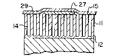
As a final point,-it should be noted that, if the film 11
is made suitably thin in a structure as shown in Fig. 1 (B), a
discontinuous (semi-reflective) metal layer may be applied to
the outer surface 15 of the film 11 rather than being
deposited by electrodeposition within the pores 14. A layer
of this kind can be formed, for example, by sputtering or
other vacuum deposition techniques. Patterned areas of the
metal layer may then be treated with the noble metal solution
and then further steps carried out as before. A typical
structure produced in this way by steps similar to those
resulting in the structure of Fig. 2 is shown in Fig. 6. In
this case, the separation between the semi-refective layer 27
and the underlying metal surface 12 is sufficiently small
(e.g. less than 1 micron), that interference takes place
between light reflected from these surfaces. The metal layer
27, being exposed and very thin, should preferably be
protected by a layer 29 of transparent material, such as a
lacquer or polymer film.
- Since the film 11 is necessarily very thin in this form
of the invention, an anodization procedure which results in a
non-porous barrier film rather than a porous film may be
employed. As was mentioned earlier, non-porous films of this
type can be produced by anodization in non-acid or weakly
acidic electrolytes and the thickness of the barrier films is
determined by the voltage used for the anodization step. Film
thickness in the range of 0.05 to 0.25 microns can be produced
in this way.
Depending on film thicknesses and the like, the patterns
produced by the present invention are sometimes dichroic or
optically variable (i.e. they exhibit different colours at
different viewing angles). This is very useful for certain
applications, e.g. security applications, because such effects
cannot be reproduced by colour photocopiers and the like.
The present invention is illustrated in mor~ ~eta ~ y
the following non-limiting Examples.
EXAMPLE 1
This Exam~le produced a well defined optically variable
coloured pattern on a non-coloured background.
An aluminum foil/polyester laminate was anodized in 15.M
H2SOs at 21C at 10V DC for a period of 3 minutes. It was then
rinsed and re-anodized in lM H3PO4 at 21'C at 10V DC for 2
additional minutes. After rinsing well, nickel was
electrolytically deposited into the porous oxide from a
standard nickel ANOLOK solution (25 g/l nickel sulphate
heptahydrate, 20 g/l magnesium sulphate heptahydrate, 25 g/l
boric acid, 15 g/l ammonium sulphate) using a 30 second
treatment at 9V AC peak, 60Hz. After rinsing and air drying a
solution containing 10 g/l PdClz was roll printed using
flexography on to the surface in a defined pattern. After
drying, the laminate was re-introduced into the sulphuric acid
solution and anodized for 130 seconds at 12.5V DC. The
laminate was then rinsed and sealed.
The resulting green pattern appeared violet when viewed
at an angle of 45~.
EXAMPLE 2
This Example produced a well defined blue pattern on a
non-coloured background (no preliminary anodizing step).
An aluminum foil/polyester laminate was anodized in lM
H3PO4 at 21 C at 10V DC for 1~ minutes. After rinsing well,
nickel was electrolytically deposited into the porous oxide
from a standard nickel ANOLOK solution (see Example 1) using a
30 second treatment at 9V AC peak, 60Hz. After rinsing and
air drying, a solution containing 2 g/l PdC12 was roll printed
using flexography on to the surface in a defined pattern.
After drying the laminate was anodized in 1.5M 21C sulphuric
acid using 12.5V DC for 90 seconds. The laminate was then
rinsed and sealed.
EXAMPLE 3
This Example produced a well defined purple pattern on a
non-coloured ~ackground (single acid and no preliminary
anodizing).
An aluminum foil/polyester laminate was anodized in lM
H3PO4 at 21C at 10V DC for 1~ minutes. After rinsing well,
nickel was electrolytically deposited into the porous oxide
from a standard nickel ANOLOK solution (see Example 1) using
a 30 second treatment at 9V AC peak, 60Hz. After rinsing and
air drying, a solution containing 2 g/l PdCl2 was roll printed
using flexography on to the surface in a defined pattern.
After drying, the laminate was anodized in the original acid
using 12.5V DC for 8 minutes. The laminate was then rinsed
and sealed.
EX~PLE 4
This Example produced a well defined opcically variable
pattern on a coloured background.
An aluminum foil/polyester laminate was anodized in lM
H3PO4 at 21-C at 15V DC for 2 minutes. After rinsing well,
- nickel was electrolytically deposited into the porous oxide
from a standard nickel ANOLOK solution (see Example 1) using a
20 second treatment at 12V AC peak, 60Hz. After rinsing and
air drying, a solution containing 0.5 g/l AuCl was roll
printed using flexography on to the surface in a defined
pattern. After drying, the laminate was anodized in 1.5M 21'C
sulphuric acid using 15V DC for 110 seconds. This period of
anodizing was interrupted at the 10 second mark, at which time
the laminate was removed and then immersed in a 300ppm PdSO4
solution for 1 minute. After anodizing the laminate was
rinsed and sealed.
The resulting pink pattern changed to yellow when viewed
at an angle of 45-. The background colour was also pink but
it was less saturated than the pattern.
EXAMPLE 5
This Example produced a random bronze dot/streak pattern
on clear architectural class 10 aluminum extrusion.
Alloy 6063 extrusion of the type used for framing
pictures was caustic etched and anodized in 1.5M HzSO4 at 21-C
at 16V DC for a period of 30 minutes to produce a 10 micron
anodic film. It was then rinsed and reanodized in lM H3PO4 at
~U ~ l~ 1
21~C at 15V DC for 3 additional minutes. After rinsing well,
nickel was electrolytically deposited into the porous oxide
from a standard nic~el ANOLOK solution (see Example 1) using a
25 second treatment at 12V AC peak, 60Hz. After rinsing and
air drylng, small droplets of solution containing 5 g/l PdCl2
were splashed onto the medium bronze surface. The extrusion
was then allowed to soak in an acid (pH 2) rinse water for 20
minutes, during which time all the non-contacted metal
deposits leached from the film. The extrusion was then sealed
in boiling water.
EXAMPLE 6
This Example produced a defined, highly saturated
blue/grey pattern on clear architectural class 10 aluminum
extrusion.
Alloy 6063 extrusion of the type used for framing
pictures was caustic etched and anodized in 1.5M H2SO4 at 21C
at 16V DC for a period of 30 minutes to produce a 10 micron
anodic film. It was then rinsed and reanodized in lM H3PO4 at
21C at 15V DC for 3 additional minutes. After rinsing well,
nickel was electrolytically deposited into the porous oxide
from a standard nickel ANOLOK solution (see Example 1) using a
75 second treatment at 12V AC peak, 60Hz. After rinsing and
air drying, a solution containing 0.5 g/l AuCl was roll
printed on to the blue/grey surface using flexography in a
defined pattern. The extrusion was then allowed to soak in 5%
V/V HNO3 for 4 minutes, during which time all the non-contacted
metal deposits leached from the film. The extrusion was then
sealed in boiling water.
EXAMPLE 7
This Example produced a brushed-on coloured pattern
(purple) on clear architectural class 10 aluminum extrusion.
Alloy 6063 extrusion of the type used for framing
. pictures was caustic etched and anodized in 1.5M H2SO4 at 21 C
at 16V DC for a period of 60 minutes to producs a 20 micron
anodic film. It was then rinsed and reanodized in lM H3PO4 at
21-C at 10V AC for 3 minutes followed ~y 10V DC for 1 minute.
After rinsing well, nickel was electrolytically deposited into
204~16~
the porous oxide from a standard nickel ANOLOK solution (see
Example l) using a 25 second treatment at 9V AC peak, 60Hz.
After rinsing and air drying, a solution containing 0.5 g/1
PdCl2 was brushed on to the surface in well defined areas.
After air drying, the work piece was anodized in the original
sulphuric acid solution at 10V DC for a period of 120 seconds
It was then rinsed and sealed in boiling water.
EXAMPLE 8
This Example produced a brushed-on dual tone bronze
pattern on coloured architectural class 20 aluminum extrusion
Alloy 6063 extrusion of the type used for framing
pictures was caustic etched and anodized in 1.5M H2SO~ at 21C
at 16V DC for a period of 60 minutes to produce a 20 micron
anodic film. It was then rinsed and reanodized in lM H3PO4 at
21C at 10V AC for 3 minutes, followed by 10V DC for l minute
After rinsing well, nickel was electrolytically deposited into
the porous oxide from a standard nickel ANOLOK solution (see
Example 1) using a 25 second treatment at 9V AC peak, 60Hz.
After rinsing and air drying, a solution containing 0.5 g/l
PdCl2 was brushed on to the surface in well defined areas.
It was then rinsed and sealed in boiling water.
EXAMPLE 9
This ~xample produced a well defined optically variable
pattern that had been transferred from the aluminum host to a
transparent polymer material.
AA5657 aluminum sheet was cleaned then anodized in
1.5M H2SO4 at 21C at 10V DC for a period of 1 minute. It was
then rinsed and re-anodized in lM H3PO4 at 30/C at 10V AC for
1.5 minutes. After rinsing well, nickel was electrolytically
deposited into the porous oxide from a standard nickel ANOLOK
solution (see Example 1) using a 25 second treatment at 9V AC
peak, 60Hz. After rinsing and air drying, a solution
containing 0.5 g/1 PdC12 was flexographically printed onto the
surface in a well defined pattern. After air drying, the
panel was then anodized in the sulphuric acid bath for 140
seconds at 12.5V DC and subsequently transferred back to the
phosphoric bath, during which time a peelable membrane was
L6~
created by anodizing at 12.5V DC for 10 seconds and then
reducing the voltage ln stepwise fashion until, after 2.5
minutes, the applied voltage was zero. The panel was allowed
to soak for an additional 1.5 minutes before it was removed,
rinsed and drled. A transparent polymer was then heat sealed
to the surface and the panel was subsequently peeled away
leaving the porous oxide containing a patterned deposit on the
polymer. The interference colour in the patterned areas was
regenerated by vacuum depositing a thin metal film on to the
surface of the membrane.
The patterned plastic film was green, changing to violet
when viewed at a 45 angle.
EXAMPLE 10
This Example produced a well defined optically variable
pattern on a coloured background.
An aluminum foil/polyester laminate was anodized in lM
H3PO4 at 21C at 15V DC for two minutes. After rinsing well,
nickel was electrolytically deposited into the porous oxide
from a standard nickel ANOLOK solution (see Example l) using
a 20 second treatment at 12V AC peak, 60Hz. After rinsing and
air drying, a solution containing 0.5g/1 PtCl2 was roll printed
using flexography onto the surface in a defined pattern. At
this time, the laminate was immersed in 100 ppm PdSO4 for 1
minute. The laminate was then anodized in 1.5M, 21'C H2SO4
using 15V DC for 120 seconds. After anodizing, the laminate
was rinsed and sealed.
The resulting pink pattern changed to yellow when viewed
at an angle of 45'C. The background colour was also pink, but
it was less saturated than the patterned area.