Note : Les descriptions sont présentées dans la langue officielle dans laquelle elles ont été soumises.
1
PATENT
_g_
METHOD AND APPARAT~7S FOR TRANSMITTING A SIGNAL
WITH AN OFFSET WHICH FOLLOWS A_RECEIVED SIGNAL
BACKGRQUND OF THE INVENTION
Field of the Invention
~ The present invention generally relates to
communication-systems and, more particularly, is
directed to a communication system having a reference
reception carrier frequency which differs from and ,
follows a reference transmission carrier frequency.
Descrintian of the Prior Art
A TDMA (time division multiple access) system is
known as one type of digital cellular communication
systean in which a base station and a mobile station
are connected via radio waves. According to this
5 TDMA system, six receiving slots, for example, are
provided for every channel of the 900 MHz band and in
each mobile station an incoming signal in one of the
six slots is received for a period of 20 milliseconds
at intervals of 3.20 millisec~nds. Six transmission'
slots are similarly provided for every channel, end
in each mobile station an outgoing signal in' one of
the six transmission slots is similarly transmitted.
A reference receiving Barrier frequency and a
reference transmitting'carrier frequency inwa single
z5 - mobile station,are different from each other. By waY
of example, a frequency 45 MHz lower than the
reference receiving carrier frequency is employed as
the reference transmitting carrier frequency.
When the mobile station is moved, an offset
frequency occurs in the actual received carrier
'frequency due to the Doppler effect. Also, if the
oscillatian frequency of a,reference r~scillator in.
the base station, wYiich uses a quartz crystal, is not
correct, then an offset frequency will also occur.
PATENT
-2-
In the mobile station, the offset frequency of the ,
transmission carrier frequency must be maintained
i~rithin a band ~200 Hz from the reference transmitting
carrier frequency.
For this reason, it has bean proposed that the
mobile station be provided with a PLL (phase locked
loop) which is locked to the reception carrier
frequency of the received signal to thereby produce
the transmission carrier signal. However, since the
received signal is a burst signal which is received
for 20 milliseconds at intervals of 120 milliseconds,
it is very difficult to lock the,PLL to the reception
carrier frequency of the received signal, as the lock
frequency must be determined during a short periad of
time (20 milliseconds) and maintained for a period of
100 milliseconds between received signals, and the
transmission offset frequency must be maintained
within the band ~200 Hz from the reference
transmitting carrier frequency.
OBJECTS AND SUMMARY OF THE INVENTION
Accordingly, it is an object of the present
invention to provide an improved communication system
in which the aforementioned shortcomings and
disadvantages encountered with the prior art can be
substantially eliminated.
More specifically, it is an object of the
present invention to provide a communication system
in which an outgoing signal has a transmission offset
frequency which follows a reception offset frequency,
so that t2xe actual transmission carrier frequency of
the outgoing signal follows the actual reception
carrier frequency of the received signal and can be
transmitted with satisfactory responsiveness and
ease,
PATENT
-3-
It is another object of the present invention to
provide a transmitting and receiving apparatus for a
digital cellular type communication system.
According to an aspect of the present invention,
a transmitting and receiving apparatus for
transmitting and receiving signals with a reference
reception carrier frequency which differs from,a
reference transmission car~cier frequency is comprised
of a reception offset frequency detecting circuit for
1p detecting an offset frequency of a present reception
carrier frequency of a received signal relative to
the reference reception carrier frequency, a
multiplier for mul~,iplying a, transmissie~n signal of
the reference transmission carrier frequency with a
frequency signal of: a detected offset frequency, and
a transmitting circuit fox transmitting an output
signal. of the'multiplier as the transmission signal
of a present transmission carrier frequency.
The features and advantages described in the
specification are not all inclusive, and many
additional features and advantages will be apparent
0 one of ordinary skill in the art in view of the
drawings, specification and claims hereof. Mereover,
it should be noted that the language used in the
specification has been principally selected for
readability and instructional purposes; and may not
have been selected to delineate or circumscribe the
inventive subject matter, resort to the claims being
necessary to determine such inventive subject matter.
BRIEF DESCRIPTLON OF THE DRAWINGS
Fiq. 1 is a block diagram showing an embodiment
of a transmitting and receiving system according to
the present invention;
-4-
PATENT
Fig. 2 is a block diagram showing a modulating
circuit used ih the present invention; and
Figs. 3I to 3III are diagrams showing the
encoding operation of the modulating circuit of Fig.
2.
DETAILED DESCRIPTION OF THE PREFERRED E~IBODI3riENT
Figures 1 'through 3III o~ the drawings depict
various preferred embodiments of the,present
invention for purposes of illustration only. One
20 skilled in the'art will readily recognize from the
following discussion that alternative embodiments of
the structures and methods illustrated herein may be
employed without departing from the principles of the
invention described herein.
25 Fig. 1 shows an embodiment of a transmitting arnd
receiving system according ~o the present invention:'
In this,embodiment, the present invention is applied
to a TDMA digital communication system in which the .
base station and the mobile station are donnected via.
radio-waves: Six receiving slots, for example, are
provided for every channel of the 900 l~lHz band, and a
mobile station receives an incoming sie~nal in one
slot thereof at intervals of 220 milliseconds for a
poriod'of 20 milliseconds. Six transmission slots
~5 are similarly provided for every channel, and a
ynobile station transmits an outgoing signal in one
slot thereof caith a similar time and interval. The
reference receiving carrier-frequency and the
reference transmitting carrier frequency in a single
30 mobile station are different from each other.
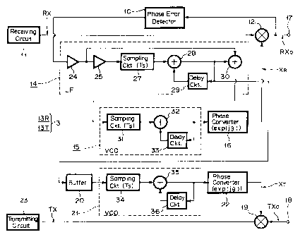
Fig..2 shows how the signal processing occurs in
the present invention with a.digital signal processor
in a mobile station (i.e., a mobile telephone) in the
form of a block diagram. 'As shown in Fig. 2, a
" CA 02042563 2000-09-08
-5-
signal RX received by a receiving circuit 11 is
supplied through a multiplier 12 to a phase error
detector 10. This phase error detector 10 produces
only the imaginary part of the signal supplied
thereto. The output of the phase error detector 10
is supplied to a loop filter (LF) 14 of a phase
locked loop (PLL) 13.
The PLL 13 is composed of a PLL 13R and a PLL
13T. The PLL 13R is comprised of the loop filter 14,
a VCO (voltage controlled oscillator) 15 and a phase
converter [exp (jB)] 16. The PLL 13T is similarly
comprised of the loop filter 14, a VCO 21 and a phase
converter [exp (j8)] 22. The above-described phase
converters 16 and 22 generate complex sine waves
corresponding to the signals supplied thereto.
The loop filter 14 is composed of a multiplier
24 for multiplying the received signal with a
coefficient K, a multiplier 25 for multiplying an
output of the multiplier 24 by a coefficient a (where
a = K/2), a sampling circuit 27 for sampling the
output of the multiplier 25 at a sampling interval
Ts, an adder 28 which adds the output of the sampling
circuit 27 and the output of a delay circuit 29, an
adder 30 for adding the outputs of the multiplier 24
and the adder 28, and delay circuit 29, which delays
the output of the adder 28 by one sampling interval
Ts and supplies the resulting delayed signal back to
adder 28. The sampling circuit 27, the adder 28 and.
the delay circuit 29 constitute an integrator.
The VCO 15 is composed of a sampling circuit 31
for sampling the output of the loop filter 14,.that
is, the output of adder 30, again at a sampling
interval Ts, an adder 32 for adding the output of the
sampling circuit 31 and the output of a delay circuit
33, and delay circuit 35, which again delays the
PATENT
_6_
output of adder 32 by one sampling interval Ts and
supplies the resulting delayed signal back to adder
32. Thus, the VCO 15 also constitutes an integrator.
The output of the VCO 15,-that is, the~output of
adder 32, is then supplied to the phase converter 16,
in which the phase thereof is determined. The output
of phase converter 16 is supplied to multiplier l2.
The VCO 21 is supplied with a signal from the
loop filter 14, that is, the output of the adder 23,
through a buffer 20, and is composed of a sampling
circuit 34, again having a sampling interval Ts, an
adder 35 for adding the output of he sampling
circuit 34 and-the output of a delay circuit 36, and
delay 'circuit 36 which again delays the output of
adder 35 by one sampling interval Ts and supplies the
resulting delayed signal back to adder 35, thus again
constituting an integrator.
The VC0 21 may alternatively be supplied with
the output of the loop filter 14, that is, the output
of adder 30, through the buffer 20.
The output of the VCO 21, that is, the output of
the adder 35, is then supplied to the phase converter
22, in~which the phase thereof is determined, and the
output of phase converter 22 is fed to a multiplier
29.
Assuming that FR represents the actual received
carrier frequency of the received signal RX detected
by the receiving circuit 11 {that is, the signal
received by the mobile station from the signal
transmitted from the base station), then the actual
received carrier frequency FR is expressed as
FR = RFn i- vF
where RFp is the reference reception carrier
frequency and of is the offset frequency.
,., r ~, j9 Y '
PATENT
_7_
The signal RX obtained from the receiving
circuit 11 is supplied through the multiplier 12 and
the phase error detector 10 to the loop filter 14, in
which an angular frequency w of the offset frequency
~F is detected, and this detected angular frequency w
is supplied to the VC0 15, in which the angle B is
detected. The angle a is then supplied to the phase
converter 16 which then generates a frequency signal
xR of the offset frequency ~F, and this frequency
to signal x~ is supplied to the multiplier l2, where it
is multiplied with the received signal RX, so that a
received signal RXO, having the reference received
carrier frequency FR~, is obtained at the outpwt
terminal l'7. This received signal RXO is supplied
Z5 to, and demodulated by, a demodulator (not shown) to
provide an audio signal.
Another angular frequency w' (the output of the
v adder 28) of an offset frequency aF' detected by the
integrator formed of the elements 27, 28 and 29
2p within the loop filter 1~ is supplied to the VCO 21,
and an angle ~' is detected. This detected angle 9'
is supplied to the phase converter 22 which generates
a frequency signal xT of the offset frequency aF'
This frequency signal x~ is supplied to multiplier
25 1g, where it is multiplied with a transmission signal
TXO, supplied from a terminal 18 and having a
reference transmission carrier frequency FTC, to
provide a transmission signal TX having an actual
transmission carrier frequency FT. This transmission
30 signal TX is transmitted to the base station from a
transmitter 23.
Assuming that FT represents the actual
transmission carrier frequency of the transmission
signal TX, then FT is expressed as
35 FT = FTC ~ ~F'
PATENT
-8-
where FTC is the reference transmission carrier
frequency.
The angular frequency w supplied to the VCO 15
must follow the received signal and must thus be the
output of the adder 30. T~owever, the angular
frequency w' supplied to the VCO 21 need not follow
the received signal so that the signal--to-noise (S/N)
ratio can be improved by utilizing the output of the
adder. 28, which has the. low noise of the received
~10 signal, before additional. noise is added by the adder
30: The difference between the angular frequencies w
and w' is negligible in comparison to the difference
between the transmission and reception frequencies.
According to the above communication system,
15when the reference reception carrier frequency FRO
and the reference transmission carrier frequency FTo
are different, the offset frequency oF' of the actual
reception carrier frequency FR of the received signal
RX relative to the reference, reception carrier
20 frequency FRS is detected by the PLL 13R and the
frequency signal x~ of the thus detected offset
frequency dF' is multiplied with the transmission
signal TX~, which has the reference transmission
carrier frequency FT~, by the multiplier 19 to
25 ' produce the transmission signal TX which is
transmitted with. an actual transmission carrier
grequency FT: Thus, the transmissioxi signal TX has
an actual transmission carrier frequency FT with the
same transmission offset frequency 0F° as the
30 reception offset frequency OF', and can be
transmitted with e~ccellent responsiveness and ease.
Similarly, the offset frequency eF of the actual
reception carrier frequency FR of the received signal
RX relative to the reference reception carrier
35 frequency FRo is'detected by the;PLL~ 1.3R and the
_g_
frequency signal xR of the thus detected offset
PATENT
frequency of is provided and then multiplied with the
transmission signal RX of the actual reception
carrier frequency FR by the multiplier 12 to produce
the reception signal RXO of the reference reception
carrier frequency FRo. Thus, even when the actual
reception carrier frequency FR of reception signal RX
contains the offset frequency aF, the audio signal
can be demodulated with the same demodulation
characteristic as that of a reception signal RXO of
the reference reception carrier frequency FRo by the
demodulating circuit.
This embodiment uses a ~c/4 shifted QPSK
(quadrature phase shift keying) modulation circuit
which is shown in Fig. 2. However, the present
invention is not limited 'to the above modulating
circuit and can be applied to either an analog
communication system or a digital communication
system.
As shown in Fig. 2, a serial digital audio
signal bm from an input terminal, 1 is supplied to a
serial-to-parallel converter 2, where it is converted
~o parallel digital signals KR and Y~ of 2 bits and
then supplied to a differential phase encoder 3:
. The encadir~g'of the differential phase encoder 3
will be described with reference to Figs. 3I to 3III.
As shown in Fig: 3I, points A (1, 1), B (-1, 1);
~ (-1~ ~1)_ and D (1; --1~ on. the perpendicular I axis
(real axis) and Q axis (imaginary axis) are
determined. Then, as shown in Fig. 3II, points
a (1, 1) , b (-1, 1) , c (-°1; -1.) and d j1, -1) on the
perpendicular I' axis (real axis) and Q' axis
(imaginary axis), which result from rotating the
ortYxogonal I axis and Q axis coordinates by 45
degrees (~t/4), are also determined.
~r~;~~~~~~
PATENT
-10-
When the I' axis and Q' axis coordinates are
moved in parallel and superimposed on the I axis and
Q axis coordinates so that their origins coincide
with each other, the coordinates of the points a, b,
c, and d on the I' axis and Q' axis coordinates on
the I axis and Q axis are presented as a (0, ~),
b (-~I 0), c (0' -r) and d (~, 0).
The encoded outputs I~ and Q~ of the encoder 3
are-then moved from any one of the points A through D
' on the I axis.and Q axis coordinates to any one of
the points a through d in accordance with the outputs
X~ and Y~ of 2 bits fr~am the serial-to-parcellel
converter circuit 2 and moved from any one of the
points a to d to any one of the points A to D in
response to the outputs X~ and YR of 2 bits of the
serial-to-parallel converter circuit~2. The
movements between any one of the points A to D and
any one of the points a to d are represented in
Fig: 3TII. Such movements never pass through the
origin O.
The movements between any one of the points A to
D on the I axis arid Q axis codrdinates and any one of
the points a to d on the I' axis and Q° axis
coordinates can be expressed by the change 0~ o~_the
angles of straight lines connecting the respective
points and the origin O.
Accordingly, a relafi.i'on between the outputs X~,
Yy~ and the difference a~ will be represented on the
following truth table.
(PATENT
-11-
XR Y~
1 1 -37~ / 4
0 1 37!/4
0 0 7r/4
1 0 -n/4
The encoded outputs.l~ and QR are respectively
supplied through baseband filters 4a and 4b to
modulators (multipliers) 5a and 5b, where a carrier
from a carrier generator 6 and a carrier whose phase
is shifted by 90 degree from the former carrier by a
90 degree phase shifter 7 are modulated (multiplied)
with the respective encoded outputs. The outputs are
then added by an adder 8 and output from an output
terminal 9 as a digital modulated signal.
Thus, the present invention as described above
is a communication system in which the reference
reception carrier frequency and the reference
transmission carrier frequency are different. An
offset frequency, which is the difference in the
.20 aG~ual reception carrier frequency of the received
signal relative to the reference reception carrier
frequency, is detected. The frequency signal of the
thus detected offset frequency is multiplied with the
transmission signal. of the reference transmission
carrier frequency to obtain a transmission signal Uf
an actual transmission carrier frequency which has an
offset frequency relative to the reference
transmission carrier frequency which follows the
offset frequency of the received signal. The
transmission signal, of can then be transma.tted with
satisfactory responsiveness and with ease.
From the above description, it will be apparent
that the invention disclosed herein provides a novel
~~~~~~~~~
PATENT
_~.z_
and advantageous apparatus for a mobile communication
system.
The foregoing discussion discloses and describes
merely exemplary methods and embodiments of the
present invention. As will be understood by those
familiar with the art, the invention may be embodied
in other specific forms without departing from the
spirit or essential characteristics thereof. for
examgle; different specific circuits could be used,
to in.either the analog or digital domain. Accordingly,
the disclosure of the present invention is intended
to be illustrative, but not limiting, of the scope of
the invention, which is set forth in the following
claims.