Note : Les descriptions sont présentées dans la langue officielle dans laquelle elles ont été soumises.
2~
SPECIFICATION
Phase Shifter Utilizing ~ybrid Element
. . .
BACXGROUND OF TXE I NVENT I ON
.
Field O~ the Invention: -
The present invention relates to a phase shifter for
shifting a si~nal in phasP and particularly to a hybrid type
phase shifter.
Description of the Relat~d Art: -
In the past, various type phase shifters have been used.
They are being important with development o~ the electrical
communication.
For e~ample, the satellite communica~ion re~uires an
antenna ~or tracking a satellite. Partlcularly, a satellite
trackin~ antenna which is mounted on a mGver such as motorcar
or the like is required to be reduced in size and electric
power consumption. It is thus believed that the satellite
tracking antenna on the mover is preferably a phas~d array
antenna. The phased array antenna is required to control the-~-
phase for each of antenna elements which form an array.
Therefore, the phase shi~ter becomes one of very important
components for the phased array antenna.
Phase shifters which are used in such a phased array
antenna and the like include digital phase shifters which i.s
adapted to change the amount of phase shift from one to
another by on-off controllin~ a switch. The digital phase
shi~ters are known to be of loaded ~llne type, swi~ched line
type, hybrid type and so on. Among them, the hybrid type
phase shifter is preferred since it has a relatively simple
.. .. .. , ,:
.
~2~7
structure for providing any amount of phase shift.
On the other hand, the digital phase shifters utilizes a
switch for selecting the amoun~ o~ phas2 shift, which may be
a diode type or ~ield ef~ect transistor (FET) type switch.
FET type switch is believed to be particularly suitable for
use in such an antenna as mounted on the mover such as
motorcar or the like, since the FET type switch has a
necessary power lower than that o~ the diode type switch in
the order o~ several figures and may include a simplified bias
circuit without any capacitor for cutting off DC.
In other wor~s, antenna systems on motorcars or other
movers requ.ire an electrical power consumption a~ low as
possible sinCe the limited capacity of batt~ry must be
eectively utilized. The antenna systems, which are used in
the motorcars or other movers, must be of a construction as
simple as possible since they are used under severe
conditions such as vibrations associated with the running
vehicles, intensive changes of temperature and so on.
It is therefore preferred that a hybrid type phase
shifter having a FET switch is used as a phase shi~ter
mounted on the mover~
One example of the conventional hybrid phase shi~ters
with a switch for selecting the amount of phase shift is
shown in Figure 17. The hybrid phase shifter comprises a
three dB hybrid element 10 in which an input signal is
divided into two output signals of equivalent magnitude, and
two phase shift regulating circuits 12.
The hybrid element 10 includes an input terminal 10a
receiving an input signal and an isolation term.inal 10b
providing an output signal. The hybrid element 10 also
~. ' ' , .
~2~
includes a coupling terminal 10c and a -through terminal 10d.
The two phase shift reyulating circuits 12 are connected with
the coupling and through terminals lOc, lOd in the hybrid
element 10.
The two phase shift regulating circuits 12 are of the same
construction which comprises a first line 12a having one
opened end and a second line 12b cascade connected between
the other end of the first line 12a and a switch 12c.
The functional principle of -this phase shifter will be
described in connection with Figure 18 which is a Smith chart.
There is first considered the reflection coeEficient r
in the switch 12c, which is one viewed from a reference plane
C to the switch side. Ideally, the reflection coefficient r
is equal to -1 when the swi.tch 12c is ON and equal to one
when the switch 12c is OFF. If the switch 12c is of FET
type, however, it includes an induction component and a
capacity component. As shown in Figure 18, thus, the
reflection coefficient r is in a position r Con which is
substantially equal to -1 and shifted clockwise due to the
induction component if the switch 12c is ON. On the other
hand, if the switch 12c is OFF, the reflection coefficient r
is in another position r Coff which is substantially equal
to one and shifted clockwise due to the capacity component.
It is secondly considered the reflection coefficient r
which is viewed from a reference plane D including the second
line 12b (characteristic impedance Z0) to the switch side.
I~ the characteristic impedance of the line 12b is equal to
50Q , the reflection coefficient r is in the respective
positions r Don and r ~off when the switch 12c is ON and OFF,
in which positions the retlection coefficient r in the
. .
reference plane C is rotated to the side of power source
~cloc~wise) by the electrical length of the line 12b while
maintaining its magnitude constant.
It is ~urther considered the reflection coe~ficient r
which is viewed from a reference plane E including the first
line 12a. The reference coefficient r is rotated on a
constant conductance circle toward the side of power source
(clockwise) to a position r Eon or r Eoff in either time
when the switch 12c is ON or OFF. In other words, the
reflection coefficient r viewed from the reference plane E
when the switch 12c is ON and OFF is rotated on the constant
conductance circle which is determined depending on the
position of the reflection coefficient r viewed from the
reerence plane D.
Therefore, the reflection coefficient r on ON and OFF in
the switch 12~ can be determined by varying the first and
second lines 12a, 12b in length and other parameters. As a
result, a difference ~ between phases when the switch 12c
is ON and OFF becomes the amount of phase shift at the output
terminal lOb. When the switch is -turned on or off, the
amount of phase shift in the phase shifter can be changed
from one to another by setting the first and second lines
12a, 12b at predetermined lengths.
However, the aforementioned phase shifter constructed in
accordance with the prior art has the following problems:
(A) The amount of phas~ shift can be set only by
adjusting both tbe ~irst and second linQs 12a, 12b. This
adjustment is very difficult. More particularly, the
adjustment of the reflection coefficient r on the constant
conductance circle by regulating the length of the ~irst line
i .
,
., .
~t~
12a should be combined with the adjustm~nt o~ the length of
the seco~d line 12b. It is extremely difficul~ to find a
proper combination of ]ength between the first and second
lines 12a, 12~.
(B) Generally, the FET switch has less property in its
ON state than that of the OFF state. This fact is not well
considered in the conventional phase shifter as described.
Thus, the phase shifter will have a loss substantially
increased from that of the OFF state. Such an increased
difference of loss between the ON and O~F states of the phase
shifter is very detrimental for the application of the
aforementioned phased array antenna.
(C) Although the functional principle of the prior art
has been described as to a single requency, it must be
measured through the entire frequency band actually used
therein. The aforementioned phase shifter has a possibility
in which the fre~uency band is extremely narrowed depending
on the case. It is very difficult to find under what
condition the frequency band can be widened.
- Although some other configurations in addition to the
aforementioned phase shifter are known in the art, none of
them could overcome the above three problems and set any
desired amount of phase shift.
In order to overcome all the problems in the prior art~
an object of the present invention is thus to provide a
digital phase shifter which can set any desired amount of
phàse shift very simply.
SUMMARY OF THE INVENTION
,_ . .
In accordance with the present invention, as shown in
Fi~ure 1, a phase shifter comprises a h~brid element 20 for
receiving an inPut signal and outputting a phase shifted
signal, a switch ~2b connected with the hybrid element 20 and
adaRted to provide a given shift to the phase, and a
distribute~ constant line 22a connected in parallel with the
switch ~2b and having a preselected characteristic
impedance. The phase shifter is adapted to shift the phase
o the output signal by turning the switch 22b on or off.
The distributed constant line 22a may be a microstrip
line structure comprising a dielectric plate 14, a ground
conductive surface 16 on one side of the dielectric plate 14
and a conductive line 18 on the other side of the dielectric
plate 14, as shown in Figure 19. Alternatively, the
distributed constant line 22a may be a tri-plate strip line
structure comprising a dielectric plate 14, ground conductive
surfaces 16 on the opposi~e sides of the dielectric plate 14
and a conductive line 18 inserted into the interior of the
dielectric plate 14.
In such a manner, the present invention provides the
switch ``22b connected in parallel with the distributed
constant line 22a. By varying the length of the distributed
constant line 22a in the range of 0 to ~ ~4, therefore, the
reflection coefficient r as viewed from the reference plane
B to the switch side can be changed from a short circuit
r =-1 to a value corresponding to that obtained when only the
switch 22b is provided. Only by varying the length of the
distributed constant line 22a, thus, a difference of phase
between the ON and OFF states in the switch 22b, that is, an
amount of phase shift in the phase shifter can be set at any
proper level.
;`' :
.~
If the distributed constant line 22a is connected in
parallel with the switch 22~, the reflection coef~icient can
be increased when the switch 22b is in its ON state. Even if
the switch 22b is of FET type having less ON characteristic
than OFF characteristic, the loss in the switch 22b when it
is turned on can be decreased to reduce a differenti21 loss
between the ON and OFF states in the switch 22b~ This
decreases any limitation for the application of the phase
shifter.
If the width of the distributed constant line 22a is
decreased, the characteristic impedance thereof can be
increased. The increased characteristic impedance in the
distributed constant line 22a provides less influence to the
amount o~ phase shift in the phase shifter. Thus, if the
phase ~hifter is applied to a signal having a ~requency of
about 5GHz and when the distributed constant line ~2a has a
high characteristic impedance exceeding 50Q , the phase
shifter can have a sufficiently increased specific band~width.
In accordance wlth the present invention, the lower limit
of the band width--can be determined not to decrease the band
width extremely.
If the switch 22b is of FET type with any resistance
located in a line between the gate thereof and the bias
terminal, the impedance viewed from the drain to the gate can
be increased. Thus, a high frequency wave leaking from the
drain of the FET to the gate thereof can be reflected to
reduca any loss when the FET is turned ofE.
In the phase shi~ter constructed according ko the present
invention, a signal inputted to the hybrid element 20 through
the input terminal 20a is phase shifted and outputted from
~2~
the output terminal 20b. The phase in the output signal can
be varied by tuniny the switch 22b on or off.
In accordance with the present invPntion, the amount of
phase shift determined by turning the switch 2~b on or off
can be very e~ficiently set. The adjustment of the phase
shi~t will be described below with reference to Fisure 2
which illustrates a reflection coefficient.
There is first considered a reElection coefficient r in
the switch 22b (e.g. FET) when viewed ~rom the reference
plane A to the switch side. As in the prior art mentioned
above, the reflection coefficient r is brought into positions
r Aon and r Aoff respectively having inductive and
capacitive components near -1 and 1 depending on the ON and
OFF states of the switch 22b.
If the length of the distributed constant line 22~ is
equal to zero, this means that a short-circuiting occurs at
the top end of the switch 22b. Thus, the reflection
coefficient r must be in a position r --1, irrespective
of the state o~ the switch 22b.
There is next considered a reflection coefficient r Bon
viewed from the reference plane ~ to the switch side if an
FET type switch 22b is connected in parallel with the
distributed constant line 22a and when the switch 22b is
turned on.
This can be conveniently illustrated by an admittance
chart. When the switch 22b viewed from the re~erence plane B
to the switch side is turned on, an admittance Y~on (-ltZBon)
can be represented below. Now assume that an admittance
between the source and drain of the FET switch 22b in its ON
state is Yon and the characteristic admittance in the
~26L~
distributed constant line 22a having its length d is Y00.
Y~on = Yon - jY00 cot (2~ d/~ )
Further assuming that the characteristic admittance
Y00~=i/Z00) is (1~50)S, the reElection coefficient r Bon as
viewed from the reference plane B to the switch side is:
r Bon = (l-~Bon)/(l+~on)
Thus, the reflection coefficient r Bon as viewed from
the reference plane B to the switch side will move from the
reflection coe~icient r Aon determined by an admittance Yon
in the swi~ch 22b to a point r =-1 along a constant
conductance circle determined by a conductance component of
Yon=l/Zon, that is, a circle passing through the points r Bon
and r =-1 and having its center on a straight line connecting
the points r =l and r =-1, by sequential-y decreasing the
length o the distributed constant line from d = ~ /4.
On the other hand, the reflection coefficient r ~off of
the switch 22b as viewed from the reference plane B to the
switch side when the switch 22b is turned off will move from
the value r Bof determined by an admittance on the OFF state
of the switch 22b to the point r =-1 along a constant
conductance circle determined by the abov admittance as in
the ON state of the switch 22b when the length of the
distributed constant line 22a decreases from ~ /4 to zero.
Since the amount of phase shift in the phase shiter is
determined by a differential phase betwe~n the ON and OFF
states of the switch 22b, any desired amount of phase shift
can be obtained only by varying the length d of the ~.
distributed constant line 22a.
As described above, the phase shifter o~ the present
invention can adjust the amount of phase shift only by
~ ~ ~L Ç~
regulating the length of th~ distributed constant line.
Thus, the adjustment can be performed to provide any desired
amount oE phase shift in a simple and accurate mannPr. Since
the adjustment of phase shift increases the reflection
coefficient in the switch when turned on, the loss on the ON
state o the switch can be reduced. Even .if the switch is of
FET type having a high resistance on its ON state, the phase
shifter can provide less loss on the ON state o the switch.
BRIEF DESCRIPTION OF THE D~AWINGS
Figure 1 is a block diagram of a phase shifter
constructed in accordance with the present invention.
Figure 2 is a characteristic diagram illustrating the
principle of the adtustment of phase shift in the phase
shifter.
Figure 3 is a block diagram illustrating the basic
construction of a range coupler used in the present invention
as a hybrid element.
Figure 4 is a block diagram illustrating the basic
construction of a broad side offset couple~-used in the
present invention as a hybrid element.
Figure 5 is a characteristic diagram illustrating the
relationship between a characteristic impedance and a
frequency band width in a distributed constant line.
Figure 6 is a characteristic diagram of a reflection
coefficient in the FET.
Fi~ure 7 is a perspective vie~ illustrating the first
embodied example o the present invention.
Figure 8 is a characteristic diagram illustrating the
reflection coefficient of the FET used.
1 0
.
~2~
Figure 9 is ~ characteristic diagram illustratin~ loss in
a 90~ phase shifter.
Figure lQ ls a characterlstlc diagram illustrating the
relationship between the length and the amount of phase
shifter in the distributed constant line.
Figure 11 is a view showing the three-bit phase shifter
in the first embodiment of the present invention.
Figure 12 is a characteristic diagram illustrating loss
in the three-bit phase shifter.
Figure 13 is a characteristic diagram illustrating the
phase shift characteristic of the three-bit phase shifter.
Figure 14 is a view illustrating the arrangement of the
second embodied example of the present invention.
Figure 14A is an enlarged plan view showing tAe primary
parts of the second embodied e~ample of the present invention.
Figure 15 is a characteristic diagram illustrating loss
in the 90 phase shifter.
Figure 15 is a characteristic diagram illustrating the
relationship between the length and the amount of phase shift
in the distri~uted constant line.
Figure 17 is a block diagram illustrating the arrangement
of a prior art phasa shifter.
Figure 18 is a characteristic diagram illustrating the
functional principle of the prior art phase shifter.
Figure 19 is a view of a microstrip line.
Figure 20 is a view of a tri-plate strip line.
DETAILED DESCRIPTION OF PREFERRED EM~ODIMENTS
-
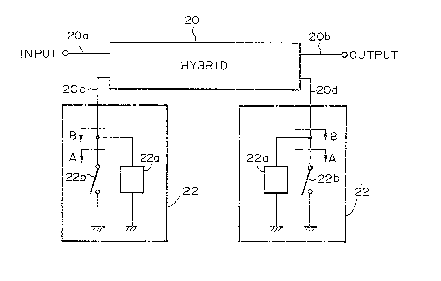
Referring to Figures 3 and 4, there are shown hybrid
elements 20 each of which comprises an input terminal 20a, an
output terminal 20b, a coupling terminal Z0c and a through
terminal 20d. The hybrid element 20 shown in Figure 3 is
a range coupler including comb-shaped microstrip lines which
are arranged close to each other and capacitive-coupled with
each other. The hybrid element 20 shown in Figure 4 is a
broad side offset coupler including two tri-plate lines which
are arranged one above another and capacitive coupled with
each other.
Phase shift regulating circuits 22 are connected
respectively with the coupling and through terminals 20c, 20d
of each hybrid element 20.
Each of the phase shift ragulating circuit 2Z comprises a
distributed constant line 22a having a characteristic
impedance exceeding 50Q and an FET switch 22b which has a
gate connected with a resistance 22c. In such an
arrangement, a signal applied to the input terminal 20a is
divided and directed into the terminals 20c and 20d through
the hybrid element 20. After the signals outputted from the
terminals 20c and 20d have been phase shi~ted respectively by
the phase shift regulating circuit 22, they are combined with
each other and taken out of the respective output terminals
20b.
The amount of phase ~hift is determined by changes of
impedance in the circuit comprising the distributed constant
line 22a and the FET switch 22b, which appear when the FET
switch 22b is turned on and off. A di~ferential phase
between the ON and OFF ~tates of the FET switch 22b can be
set at any desired level by suitably varyin~ the langth of
the distributed constant line 22a as shown by the Smith chart
of Figure 2.
1 2
., ~ .
~' ~
~;2~
In such a manner, the amou~t of phase shi~t can be set
very simpl~ a~d accurately.
The relationship between ~he characteristic impedance and
the frequency band width in the distributed constant line 22a
when this phase shifter is used as a 90 phase shi~ter for a
differential phase equal to 90 as shown in Figure 2 is
illustrated in Figure 5. In this case, the band width in
which the amount of phase shift deviates by 10 due to the
change o signal frequency is defined as a frequency band.
The change o the band width is represented rela~ive to a
reference condition in which the characteristic impedance of
the distributed constant line 22a is equal to 50Q .
Referring to Figure l, the admittance of the circuit as
viewed rom a reference plane 9 is shown to ~e a sum of an
admittance of the switch 22b as viewed from a reference plane
A and an admittance jY00 cot(2~ d/~ ) of the distributed
constant line 22a having one short-circuited end. As a
result, the characteristic impedance Z00 of the distributed
constant line 22a increases. In other words, the frequency
o the admittance in the circuit as viewed from the reference
plane B, that is, the change associated with the change in
the wavelength ~ decreases as the characteristic admittance
Y00(=1/Z00) decreases. If the characteristic impedance of
the distributed constant line 22a is increased, therefore,
the amount of phase shift will also be less changed since the
change of the admittance due to the change of the frequency
is less.
If the distributed constant line 22a is reduced in
thickness and the characteristic impedance thereof is
decreased in such a manner, the amount of phase shift will be
1 3
- - . , ~.
less changed by the changed fr~quency to increase the
frequency band width.
This efect is saturated as the characteristic impedance
becomes equal to about 10 Q . From this fact, it is
understood that if the characteristic impedance is equal to
or more than about 100Q , the frequency band width can be
increased sufficiently. In this regard, this is true for
other phase shifters other than the 90 phase shifter. It is
~hus desirable that the distributed constant line 22a has its
characteristic impedance equal to or more than 100Q .
In such an arrangement, further, the characteristics of
the phase shifter is improved to have a reflection coe~ficient
r ~on as viewed from the reference plane B when the FET
switch 22b is in its O~ state, which is near a point r =^ 1,
as shown in Figure 2. Thus, the difference of loss in the FET
switch 22b when it is turned on and off can be reduced to
decrease the limitation on the application.
In a range C (near the point r =l ) as shown by
double-headed arrow in Figure 2, the absolute value of a
retlection coefficient r Boff as viewed from the refere~ce
plane B to the switch side when the FET switch 22b is turned
off becomes smaller than that o the reflection coefficient
r Bo~f to increase the loss in the phase shifter. This is
due to the characteristics of the FET switch 22b itself.
Thus, the OFF characteristic af the FFT switch 22b must be
improved. However, the reflection coefficient when only the
FET switch 22b is turned off is not necessarily preferred, as
shown in Figure 6.
This results from any leakage of high frequency from the
drain to the gate of the FET switch 22b. In the present
1 4
invention, thus, the gate of the FET switch 22b is c~nnected
in series with the resistance 22c. As a result, the
impedance of the FET switch 22b as viewed from the drain to
the gate will increase to improve the characteristics thereof
by well reflecting any leaking wave toward the gate.
In the past, the gate characterislic of the FET has been
improved by connecting the gate thereof in series with a bias
circuit which comprises a distributed constant line having a
high characteristic impedance for the length ~ /4 and a
parallel capacitor connec~ed with the distributed constant
line. In such a prior art, however, the OFF characteristic
of the FET switch 22b can be improved only near its designed
~requency band, as seen from Figure 6.
On the contrary, the present invention can improve the
OFF characteristic o the FET switch 22b independently of the
frequency, as shown in Figure 6.
In accordance with the present invention, the phase
shifter can set the amount of phase shift at any desired
level more simply since the difference between the ON and OFF
characteristics is less in the widened frequency band.
Example 1
Figure 7 is a perspective view showing the first embodied
~xample of the present invention. This e~ample uses a range
coupler as hybrid element, as in Figure 3.
In Figure 7, a substrate 110 having a given dielectric
constant includes a copper ground surface llOa formed on the
backface thereof. The frontface of the substrate 110
includes a hybrid element 120 formed thereon by microstrip
lines. The hybrid element 120 comprises an input terminal
120a, an output terminal 120b, a coupling terminal 12Uc and a
1 ~
through terminal 120d. The coupling and -through terminals
lZOc and 120d are connected with phase shift regulating
circuits 122, respectively.
Each of these two phase shift regulating circuits 122
comprises a distributed constant line 122a and an FET 122b.
In one of the phase shift regulating circuits, the drain of
the FET 122b is connected with the coupling terminal 120c
while the source thereof is connected with the earth pad
122c. In the other phase shift regulating circuit, the drain
of the FET 122b is connected with the through terminal 120d
while the source thereof is connected with the earth pad
122c. Each of the earth pads 122c is connected with the
copper ground surface 110a through through-hole means or the
like.
On the other hand, the gate of each of the FET 122b is
connected with a bias terminal 124 through a line 124a.
The FET 122b can be turned on or off by a voltage applied to
this bias terminal 124. The FET 122b contains a monolithic
resistance located in a path extending from the gate pad to
the gate of the FET.
In this example, the substrate 110 is made o a material
having a specific inductive capacit~ equal to 10.2 ~e.g.
Trade Name Epsilum-10 or Duroid RT/6010.5) and has a
thickness equal to 1. 27mmO
On the other hand, several distributed constant lines
122a was made of various lines having the same width equal to
50 microns but of different lengths. In each of phase shifts
so formed, tha gate of each FET 122b is connected in series
with a resistance in the line 124a extending ~rom the bias
terminal 124 to the gate o~ the FET 12Zb. l'hus, the phase
1 6
.
.
. . .: :
'~
shifter comprises only a wiring pattern ~or appl~ing a bias
simultaneously to the two FET's withou~ use of any bias
circuit which comprises a 1/4 wavelength line and capacity as
generally used in the art.
The reflective characteristic between the source and
drain of an F~T 122b used in this example is shown in Figure
8. Since the monolithic resistance is used herein, the
absolute value of the re~lection coefficient when the FET
122b is turned o~ inhibits a good value substantially equal
to 1.0 between lGHz and 2GHz and further through a widened
frequency band width. On the other hand, the absolute value
of the reflection coefficient on the ON state of the FET
switch 122b will be slightly smaller than the above absolute
value, that is, equal to 0.94 which is calculated from the
val~e 2 Q Qf the ON resistance.
In the conventional phase shift regulating circuits which
have not been investigated sufficiently, it was ordinary that
differential loss of reflection between the ON and OFF states
directly influencas the characteristicæ of the pnase
shifter. In order to overcome this influence from the
differential loss of reflection, a technical perception and
trial and error were req~ired.
In accordance with the present invention, however, the
reflection coefficient on the ON state of the FET can be
increased by regulating the length of the distributed
constant line 122a when the amount of phase shift is to be
adjusted. Any difference between the ON and OFF
characteristics can be negated easily.
Figure 9 shows the magnitude of loss in the 90 phase
shifter between 55 GHz and 1.65 GHz. At 1.6 GHz, the
1 '7
.
magnitude of loss is equal to 0.49 ds on the ON state of the
FET and to 0.46 ds on the OFF state of the FET. A difference
between these values is only 0.03 dB. This means that the
phase shi~ter successfully negates the differential loss
between the ON and OFF states in the FET 122b.
In accordance with the illustrated example, a phase
shifter having any desired amount of phase shift is provided
by suitably selecting the length of the distributed constant
line 122a which is located in parallel between the source and
drain of the FET 122b~
Figure 10 shows variations in the amount of phase shift
in the phase shifter when the length of the distributed
constant line is varied into various values. In this
example, the amount of phase shift can be changed between O
and 180 ~ at the frequency 1.6 GHz by selecting the le~gth of
the distributed constant line 122a on the substrate 110
between O and 30 mm. The length o~ the distributed constant
line 122a depends on the dielectric constant, thickness or
design frequency band of the substrate 110. Even in such a
case, the present invention can provide any desired amount of
phase shift.
Figure 11 shows a phase shifting system which comprises
three 45 , 90 and 180 phase shifters connected together in
series and can provide any desired amount of phase shift or
each 45 till 360 (referred to "a three-bit phase
shitin~ system). These phase shifters used herain were
constructed in accordance with the principle of the present
invention. The loss and phase shift in the three-bit phase
shifting system are shown in Figures 12 and 13, respectively.
From these figures, it will be apparent that the loss is
'
.
,
~ s~3
in a good level ~etween 1.7 d~ an~ 2.0 d~ with a very small
range equal to 0.3 dB. The amount of phase shi~t is ranged
within + 10 ~ between 1.54 GHz and 1.66 GHz, providing a
suf~iciently widened frequency band.
Exampl e 2
_
Figu~e 14 shows an example 2 according to the present
invention. Each of FET's 122b is the same as in the first
example. This e~ample is consisted of tri-plate strip lines.
In other words, a substrate 110 compriseæ a substrate
component llOa having a specific inductive capacity of 2.2
and a thickness of 0.127 mm and substrate components llOb and
llOc each having a specific inductive capacity of 2.2 and a
thickness of O.787 mm. The outside face o each of the
substrates llOb and llOc is formed with a copper ground
surfacé layer 112b or 112c. These substrate components are
made of a material commercially available as trade name,
Duroid RT/5880.
The substrate component llOa includes wiring patterns
formed therein at the opposite sides. One of the wiring
patterns defines a hybrid element 120 on the front side of the
substrate component llOa, which in turn defines a 3dB coupler
consisting of broad side offset coupled lines. The front face
o~ the substrate component llOa includes an input terminal
120a and a through terminal 120d while the back ~ace therecf
includes an output terminal 120b and a coupling terminal 120c.
A phase shift regulating circuit 122 comprises an FET
122b and a distributed constant line 122a, as in the example
1.
Figure 14A shows an enlarged plan view of the phase shift
regulating circuit 122 (which comprises the FET 122b and the
2~`2~
distributed constant line 122a) encircled by a circle in
Figure 14 and connected with the through terminal 120d of the
hybrid element 120. The FET 122b includes three terminals,
that is, a source 122bs, a drain 122bd and a gate 122bg. The
drain 122bd is connected with ~he through terminal 120d of
the hybrid element 120. The source 122bs is connected with
an earth pad 122c while the gate 122bg is connected with a
line 124a which in turn is connected with the bias terminal
1~4.
Another phase shift regulatlng circuit Eormed on the
backside o the substrate component 110a comprises an FET
122b, the drain 122b of which is connected with a similar
hybrid element 120 formed by the other wiring pattern at the
coupling terminal 120c of the hybrid element 120. The source.
o the FET 122b is connected with an earth pad 122c which in
turn is connected with the copper ground surface layers 112b
and 112c through through-holes 132.
Since this circuit is formed of tri-plate strip lines,
the substrate component 110a is sandwiched between the
substrate components 110b and 110c. In order to receive
the thickness of the FET 122b, the substrate component 110b
includes an opening 130 ~ormed therein. Furthermore, the
perfect grounding to the earth pad 122c can be provided by
the through-holes 132 formed in the substrate components
110a, 110b and llOc.
Insertion loss in a 90 phase shi~ter constructed
according to the present invention is shown in Figure 15.
At 1.6 ~Hz, the insertion loss becomes equal to 0.58 dB
on the ON state of the FET and to 0.43 d~ on the OFF state of
the FET with a difference therebetween being equal to 0.15 dB
2 0
- : , , ,
which is small. The amount oE loss itselE also is small.
This fact means that the present invention can provide good
characteristics in phase shifter.
The relationship between the length of the distributed
constant line and the amount of phase shift in this example
is shown in Figure 16. Slmilarly, the phase shlfter can
change the amount of phase shift to 180 ~ in a range equal to
or smaller than 30 mm. It was found that the advantages of
this example are similar to the microstrip line type.