Note : Les descriptions sont présentées dans la langue officielle dans laquelle elles ont été soumises.
i~O43~338
Fi~ld of Invention
The present invention relates generally to power
lifi~rR partic~ rly adapted to provide modulation
f or an output stage of an AD~ RF i l; f i ~r . More
particularly, the invention relates to a power
amplifier i ncl~ n~ multiple stages for selectively
coupling power from a DC power supply to a load,
wh~rein responses from the multiple stages are summed
together and the number of stages that couple power to
the load is det~rmi n~d by the amplitude of a
signal source.
Backqround Art
Power; l i f i ~rR of the pulse width modulated type
are Lle~luelltly used to provide modulating inputs to an
output electrode of an output stage of a high power AN,
RF tranamitter. Some of the prior art technologies for
supplying a modulating input to an output stage of a
hilgh power AM RF i 1 i f i ~r are Class B push-pull
amplifiers and Class D pulse width modulation
; lifiF-rR. r li~ry of prior art patents ~i~Rclosin~
sulch modulation sources are Hulsey et al., ~nited
States Patents 4,747,161 a~d 4,776,036, Weaver,
4,896,372, as well as C n~5 4,140,980, Swanson
3,506,g20 and Swanson 3,588,744. In these prior art
devices, the modulating ~v~v~f~ controls the voltage
supplied to the anode, i.e., plate, or output
Z043838
2
electrode, of a power transmitting tube. Basically,
the plate DC power supply voltage of the output tube is
va~ied in response to an analog modulation source.
Typically, pulse width modulated, Class D
1 l;fiF-rs produce varying output signalg by rhiqn~in~
the on and off times, i.e., duty cycle and LL~:~Ue~1 jY,
of a switch ciulrll~u Led between a DC power supply and the
plate of the output stage . In some ins L~-~ies, the
am~?litude, as well as duration, of current and voltage
fed by the switched supply to the output stage is
varied. The variable duration current pulses are
collpled to the anode of the output stage via a low pass
filter, to substantially reconstruct the ~)ri~;niql
analog input signal to the power amplifier.
To obviate the disadvantages associated with high
voltage switching, e.g., 30,000 volts, some power
lifir,rg use multiple pulse width lAtir~n stages
controlled by phase ~ pl iq~ pulses having the same
duty cycle ; see , e . g ., U . S . Patents Swanson 4 , 4 6 8 , 6 2 6 ,
Swanson 4,164,714 and Kyrian et al 4,369,40g. In these
modulators, Ll:LeLL~:d to in the art as polyphase pulse
width modulators, the stages are switched at the same
L~ ue~uy~ but with relative phase differences. The
po~Yer f ed through the multiple stages is summed .
A disadvantage of the polyphase pulse width
modulation iqrriq- : is that usually all of the
stages are being switched simult~n~oll~ly. This results
in all of the stages being susceptible to narrow pulse
distortion, as described in Hulsey, U. S . Patent
4,776,036. Hence, a problem with the polyphase pulse
width modulation source is tha~ the modulating output
voltage i8 in certain instances not an accurate replica
of the analog signal supplied to the device. This
results in distortion of the modulating waveform, with
resulting distortion in the transmitted signal of the
A~ RF tranrmitter.
Z043838
3
I
In accordance with a f irst aspect of the
in~rention, an ~ r responsive to a source
comprises at least several stages activated only to one
of two bi-level states controlled in re8ponse to the
value of the source PY~PPil;ng a threshold
for each stage. ~3ach stage has a different threshold
arranged 80 that the stage8 change between the bi-level
states as the value of the source changes
relative to the thresholds of the dLfferent stages.
Bi--level outputs associated with the bi-level states of
the plural stages are summed together. The i, v~
is characterized by: means for ~ontin~ Rly varying
the values o~ the thresholds by a small amount
relative to a predetPrnin~d maxLmum value for the
source .
In accordance with another aspect of the inventlon,
an amplifier responsive to a source susceptible of having
changing values as a function of time~ comprises at least
several stages activated only to one of two bi-level states
controlled in response to the value of the source ~xrPP~l; ng
a threshold f or each stage . The thresholds and source are
arranged so that the stages change between the bi-level
states as the value of the source changes relative to the
thresholds of the different stages. Bi-level outputs
associated with the bi-level states of the stages are
summed together. The improvement is characterized by:
means for continuously varying the value of the threshold
relative to a median threshold by an amount that is a
function of the value of the source.
To achieve maximum linearity and minimize distortion,
the continuous variation changes linearly as a function
of time. Such a waveform is achieved
4 Z043838
with a sawtooth or triangular waveform. ~inimum
distortion is achieved if a triangular wave having a
variable f ~uen. y R8 a function of the amplitude and
frequency oi ~he source ls provided. sy varying
the threshold, partilcu1Arly in a linear manner, there
i8 a ci~nificAnt reduction in distortion ~id to
prior art devices, such as disclosed in the
aforementioned patents C'.~ with polyphase pulse
width modulation.
While distortion is relatively low in the power
lifi~r ~ rloFied in Fig. 3 of Swanson, ~403,197,
the relatively low distortion is achieved with a
corlplex aLL~lay~ t having a significant number of
corlponents wherein a voltage sum derived from the
plulral series connected stages is ~ d with the
voltage to be ~ ,1 i f ied . The resulting error signal is
cul,,v~:LLed into a digital signal for controlling several
st~ges having digital weighted output voltages.
In Woodard, 4~24,420, DC output voltages from
multiple DC sources are ~ in~rl in response to the
amplitude of an analog input signal. While this system
has relatively low distortion, it requires a large
number of c L 8 and is complex, requiring an
analog to digital . c --v '-L LeL, as well as a binary to
discrete decirlal step converter and DC power supplies
having differing voltages.
With the present invention, it has been found that
under mo~t circumstances distortion is m1nimi7sd by
ArrAn~in~ the maximum value of the continuously varying
amplitude to equal the amplitude between ad~acent
thresholds of the different stages. The ad~acent
thr~chol~c are spaced in amplitude by ArrroYi~tely the
same amount . In one : ` i L, or a low power control
lilfi~r of a second ~- ~i 1;, this causes one of
the stages to be operating in a pulse width modulating
mode while all other stages are either fully in one or
Z04383~
s
another of the states. As the amplitude of the input
signal varies relative to the thresholds, other stages
operate in the pulse width modulating mode and the
,~ ining gtages are either fully in one or the other
of the states.
It is pos~iihl~, however, for the maximum amplitude
of the constantly changing amplitude to have other
values, as long as they are in excess of the amplitude
between ad~acent thresholds and the maximum amplitude
is relatiYely small compared to the maximum amplitude
of the signal. Thus, for example, if the
masimum value of the constantly ~h~ngin~ amplitude is
twice the amplitude between ad~acent equal thresholds,
a pair of stages are simultaneously in the pulse width
modulation mode. While there may be a slight increase
in distortion in this mode, such operation has the
ad~antage of preventing errors that can occur as a
rel3ult of slight threshold differences of the various
stages .
E~ence, another way of consiaerlng the invention i8
as an amplifier responsive to a source having a value
N+k susceptible of having changing values as a function
of time wherein the amplifier comprises at least several
stages activated only to one of two different bi-level
states. ~i-level outputs associated with the bi-level
states of the stages are summed together to derive a
summed response. The i...e,,~,v~ t is characterized by:
means responsive to the source ~or activatlng the stages
so that the number of stages in one of said states is
proportional to N and at least one of the stages is
pulse width modulated. The duty cycle of the pulse
width modulation is proportional to k so tllat the average
value of the summed responses over one cycle of the pulse
width modulation is proportional to N+k, any one of said
stages being susceptible of pulse width modulation
proportional to k.
In another aspect, the invention is directed to an
amplifier responsive to a source susceptible of having
changing values as a function of time and comprises
z~3838
6
at least several stages activated only to one of two dlf l=erent
bi-level states. Bi-level outputs associated with the bl-
level states of the stages are summed together to derive a
su~mmed response that is a stepwise function of the source.
The improvement is characterized by: means responsive to
the source for activating the stages so that the number of
stages in one of said states is commensurate with the com-
bination of the value of the source and a continuously
varying signal always having a small maximum value relative
to a prede~ rmin,~d maximum value of the source.
In accordance with another feature, the ~ ~ ~,v~ nt is
characterized by activating the stages so that (a) the
number of stages in one of the states is ~roportional to
the value of the source and (b) at different times,
different ones of the stages are in first and second of
said states even though there is no change in value o
the source.
In accordance with a further feature, an ampli~ier
responsive to a source susceptible of having changing
values as a function of time comprises at least several
stages activated only to one of two different bi-level
~tates. si-level outputs associated with the bi-level
states of the stages are summed together to derive a
summed response that is a stepwise function of the source.
In response to the value of the source, there are derived
first and second ~ n~lq respectively indicating that
the number of stages in one of sald states is to increase
-and decrease. The i ~L~)v~ t is characterized by: means
responsive to the ~:~ n~s for increasing and decreasing
the number of stages in f irst and second of said states
so that the stage which has been in the first state the
longest is activated to the second state in response
to the second
Z043~38
command and the stage which has been in the second state
the longest is activated to the first state in ~esponse
to the first command, and for causing different ones of
said stages to be in the firs~ state and different ones
of said stages to be in the second state at different
times even thouqh there is no change in value of the
source .
This arrangement enables the dLfferent output
stages to be non-sourced conducting states at different
times f or the same value of the source, so
dissipation losses in the several stages are equalized
to a large extent. ~hereby, the tendency for certain
stages to overheat and become susceptible to f ailure is
substantially obviated. In other words, the load is
shared amongst the different stages to maximize
rl i f i ~r lif e .
In ACrr~,r-1Anre with one feature, the thresholds for
the plural stages are derived by a control circuit
re13pr~n~ive to DC reference voltages derived from a
voltage divider cu.. ne.;Led across tr~rminAl~ of a DC
supply. The voltage divider includes at least several
taps and the voltage at each of the taps is related to
the threshold for each stage. Each stage also
preferably inrl~ a comparator responsive to the
lin,~ar combination of (a) the source, (b) the
amplitude of a signal representing the varying values
and (c) a reference value controlled by
the voltages at the taps for deriving an output signal
having transitions for controlling the stage conducting
state .
In accordance with a further aspect of the invention,
an amplifier responsive to a source susceptible of having
changing values as a function of time comprises at least
several stages activated only to one of two different bi-
level states. si-level outputs associated with the bi-level
states of the stages are summed together to derive a
suml~ed response that is a
8 Z0~3838
stepwise function of the source. There is
included: means responsive to the source for
deriving a first indication of the number of stages that
should be in a f irst of the states and a second indication
of the number of stages actually in the first state, ana
means responsive to a comparison of the first and second
indications for controlling the length of time each of
said stages is in said first state and the number of stages
in said first state, the ill~lLUV~ t being characterized
by: said control means including means for storing a
value commensurate with the number of stages in the one
bi-leve~ state, the value stored by the storing means
being changed in response to the comparison indicating that
lS the irst indication exceeds the second indication and
the second indication exceeds the first indication.
In the preferred embodiment, the means for deriving
the first indication includes plural inpu~ elements having
only bi-level outputs controlled in response to the amplitude
of the source f~ tl1ng- a threshold for each input element.
Each input element has a different threshold. The thresholds
and source are arranged so that outputs o the input elements
change between the bi-level outputs as the amplitude of
the source changes relative to the thresholds of the different
input stages. The outputs of the input elements are summed
together .
The means ~or controlling the length of time each of
said stages ls in the first state and the jnumber of stages
in said first state includes means for changing the state
of one of said stages in response to the comparison
indicating that the first and second indications are
unequal by more than a dead band. The means for changing
the state of one of said stages includes means responsive
to the comparison for increasing and decreasing the number
of stages in the first state.
In the preferred embodiment, the means for increasing
and decreasing includes a ring modulator havlng plural
stages. The ring modulator includes a pair of shift
registers, each having an increment input
2V~1383~
and plural states, each associated with a stage. One
of the in.:L~ L Lnputs is responsive to a signal
indicating that the f irst indication exceeds the second
indication. The other increment input is responsive to
a signal indicating that the second indication exceed~
the f irst indication .
In one embodiment, the i9mrl i f i ~r i8 a power
_ 1 i fi~r and the stages are power output stages of the
po~wer Am~lifir~r~ In another ~ t, the i lifi~r
is included in a control circuit for power output
stages of a power; lifi~r. The power output stages
are activated only to sourced and unsourced states.
Control of which of and for how long the power output
stages are in the sourced and unsourced states is in
response to the sum of the outputs of the stages of the
control circuit.
Brief Description of Drawinq
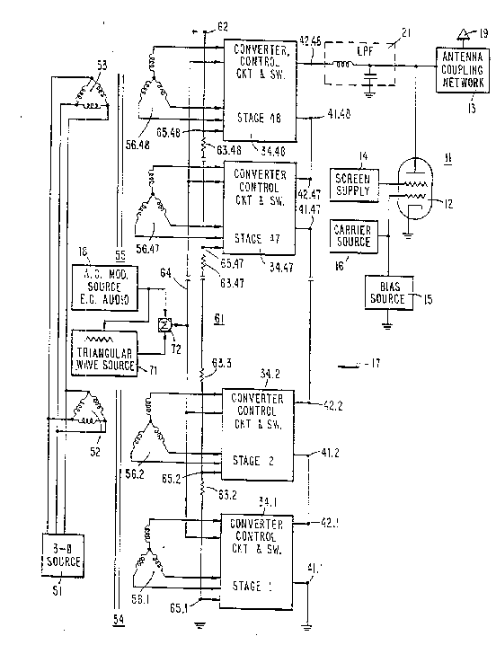
Fig. 1 is a block and circuit diagram of a
tr,~nsmitter inf~ in~ a power l~f~r~r in is~cnr~i~n~e
with one: ' 'i L of the invention;
Fig. 2 is a circuit diagram of one stage of the
1 i f i ~r illugtrated in Fig . l;
Fig. 3 is a circuit and block diagram of a
'1f~ tion of the i lifi~r wherein different stages
ar~ activated at different times in response to an AC
si~nal having the same amplitude, to derive an output
voltage having the same amplitude at the different
times; and
Fig. 4 is a block diagram of a ring modulator
in~ d in the I , 1 ~f~r of Fig. 3.
Z043838
Description of the Preferred r ' - 'i Ls
Reference i8 now made to Fig. 1 of the drawing, a
block and circuit diagram of a transmitter including an
e ~ of the present invention. The transmitter
in~l--Ae~ high power output stage 11 including tetrode
tu]be 12, antenna co~rl in~ network 13, screen supply 14,
DC bias ~ource 15 and r. f . carrier aource 16 . Bias
sollrce 15 and carrier source 16 are selected 80 that
tetrode 12 is activated to be driven in any of Class B,
C, or G. A modulation voltage is applied as the power
sul~ply voltage f or the anode , i . e ., plate , of tetrode
12 by a modulation source including modulator 17. In
actuality, modulator 17 is a high power amplifier
re~3ponsive to AC analog modulation source 18, typically
an audio, voice source that varies between a zero
voltage level and a predet~rmine~i ma2imum level.
Tetrode 12 . ~ to the outputs of sources 15 and
16, the voltage of supply 14 and the variable amplitude
DC voltage applied to plate 11 thereof to derive an
amplitude modulated wave having a center frequency
equal to that of carrier source 16. The wave derived
by tetrode 12 is applied to antenna lg by way of
antenna coupling network 13.
Power ~ lifier 17 derives a variable amplitude,
variable ~ U~ y wave that is approximately a replica
of the wave derived by source 18. The wave derived by
~11f~r 17, however, has step variations at discrete
voltage levels. Typically, the step variations are
approximately 600 volts. In one embodiment, 48
different steps subsist between the minillnum and maximum
voltages derived by ~lif1~r 17 80 the ma2imum voltage
is approximately 28,800 volts, at a power level of
about 500 kilowatts. The output of i lifi.~r 17 is
smoothed or av~L..~d by low pass filter 2~ as it is
applied to the plate of tetrode 12 80 that the tetrode
204383
11
plate voltage is a close replica of the wave of aource
18 .
In one ~ ; t, power; _-l i f i ~r 17 includes 48
different stages 34.1, 34.2, 34.3...34.46, 34.47 and
34.48; for convenience only the first two and last two
stages, i.e., stages 34.1, 34.2, 34.47 and 34.48, are
illustrated. Like components of the different
identical stages bear the same ~fl::L~ R to
the left of a decimal point, while _, Ls of the
same stage have the same reference numeral, equal to
the stage number, to the right of the decimal point.
In the following description, stage 34.1 is discussed
in detail. Since all of stages 34 are the same, the
discussion of stage 34.1 is generally sufficient for
all of the stages. The number of stages can be greater
or smaller than 48, but in any event at least several
sta~es are provided.
Responses from all of stages 34 are summed
together by adding output voltages of the different
sta~es together. The output voltages are added
tog2ther by stacking the voltages at the output
tr~inAlR of the different stages together.
Each of stages 34 is selectively in a fully
sourced, i.e., saturated, state or a non-sourced state.
Each of stages 34 is powered by a DC source having the
same voltage. While each stage is in a fully
conducting ( saturated ) state, the DC voltage applied to
the particular stage is applied to output t~rminAlR 41
and 42 of the stage. While a particular stage 34 is
non-sourced, the output voltage and output ~ -' of
th~ stage drop virtually to zero.
Output t~inAl R 41 and 42 are connected in series
between ground and the input of low pass filter 21.
~lence, t~rminAl 41.1 is yL~u~lded~ ~orminAlR 42.1 and
41.2 are connected together as are ~r~rminAlR 42.47 and
41.48, while t~rminAl 42.48 is connected to filter 21.
2043~38
12
The sum of the voltages at output t~rminAl~ 41 and 42,
as derived at t~rmi nA 1 42 . 48, is thus s~rpl i r~ as a
variable amplitude DC voltage to low pass filter 21.
DC power for each of stages 34 is derived from
three-phase AC power source 51. Source 51 drives delta
connected primary windings 52 and 53 of transformers 54
and 55 in pArAl l~l . Winding 52 drives isolated wye
cormected three-phase secondary windings 56 .1-56 . 24
while transformer 53 drives similarly connected
se~nn~lAry windings 56 . 25-56 . 48 . Primary windings 52
and 53 include taps (not shown), ad~usted 80 that the
AC current f lowing into each of stages 34 is
approximately in phase with the voltage developed
across the AC input t~rminAl~ of the particular stage;
in other words, the power factor of the power supplied
to each of stages 34 is close to unity while the
particular stage is conducting, to m~Yimi 7~ efficiency.
To these ends the taps of windings 52 and 53 are
ad justed so that there is approximately a 30 phase
shift in the current applied to the primary win~in~
relative to the current derived from secnn~lAry windings
56~1-56.48. Two different primary windings 52 and 53
are provided because of problems associated with
closely coupling more than ArFro~ tely 24 three-phase
sernn~iAri es to a single three-phase primary. Each of
stages 34 includes a full wave three-phase rectifier
(not shown) for converting the three-phase input of the
particular stage into a DC voltage having relatively
low ripple and constant amplitude.
Each of stages 34 is driven in pArA 1 1 ~l by the
output of AC analog modulation source 18. Each of
stages 34 has a different threshold for the output
voltage level of source 18. The different thresholds
are es~hl i ~h~d by connecting resistive voltage divider
61 between a positive DC voltage at t~rminAl 62 and
ground. Voltage divider 61 in~ a different tap 65
13 Z0a~383E~
or each of stages 34. Equal valued resistors 63 are
connected between ad~acent taps so the voltage
difference between adjacent taps is the same. In one
, the voltage of source 62 is 4 . 8 volts 80
the voltages at taps 65.1, 65.2.. 65.47 and 65.48 are
respectively 0, 0 .1. . . 4 . 7 and 4 . 8 volts .
The threshold values applied by taps 65 of voltage
divider 61 to stages 34 are _ ~d with an analog
voltage on lead 64. In Le~ 8e to the threshold of a
particular stage 34 being less than the voltage applied
to that stage by the voltage on lead 64 the particular
stage is activated into a fully conducting, saturated
state. In response to the threshold applied by voltage
di~vider 61 to a particular stage being greater than the
voltage applied to the stage via lead 64, the
particular sti-~ge is in a non-sourced state.
Stage 34.1 is connected to a ~ro~n~l~d tap of
voltage divider 61 so that stage 34.1 is conducting
whenever the voltage on lead 64 exceeds a zero
aml~litude, which is the vast majority of the time. The
voltage at t~rm;nAl 62, applied to stag~ 34.48, equals
the maximum voltage of source 18 . Stage 34 . 48 is
activated into a fully conducting, saturated state for
only a small percentage of the operating time of the
i lifir~r. In the ~ cll~sed ~i L, stage 34.1 is
conducting at all times except a portion of the time
while the voltage of source 18 is less than 0 . 05 volts;
stage 34 . 48 is fully conducting only a portion of the
time the voltage of source 18 exceeds 4.75 volts. When
the voltage of source 18 equals 0.0 or 4.8 volts, each
of stages 34 .1 and 34 . 48 has a 50~ duty cycler
respectively. As the voltage of source 18 varies
between slightly more than 0 . 05 volts to slightly less
thAn 4.75 volts int~ te one8 of stages 34, i.e.,
stages 34 . 2-34 . 47, are in fully conducting and non-
sourced states for variable times that prir-ri 1y are a
-
2043838
14
function of the amplitude of source 18. AB the
amplitude of source 18 increases and ~ rr~AReR the
number of fully conducting stages increases and
decreases accordingly, 80 the number of fully
conducting stages is }-AR jrAl ly a linear function of the
amplitude of source 18.
Each of stages 34 is activated between a fully
conclucting and non-sourced state as a function of the
amplitude of audio source 18, the threshold voltage
applied to the particular stage by voltage divider 61
and a factor that effectively varies the threshold of
~11 of the stages simultaneously multiple times during
eac~ cycle of source 18. The variation in effective
threshold level of each stage 34 is by an amount at
least equal to the threshold between adjacent stages.
In one conf iguration of the device which has
actually been c.,l.~Llu-;Led, the threshold variation was
equal to the difference between adjacent thresholds.
It was f ound that such variations materially reduced
the distortion of the modulating voltage applied by low
pass filter 21 to the plate of tetrode 12 relative to
the situation that would have DC-,ulL~:d without a
variable threshold. It is also feasible for the
threshold variation to be equal to the threshold of
more than one stage, as long as the thr~Rhnld variation
is only a small percentage of the maximum voltage of
source 18. If the threshold variation is twice the
thrl~Rhold between an ad~acent pair of stages 34, the
outputs of the two stages are a~ Gd and eliminate
control problems for the voltages at taps 65.
The variable threshold for stages 34 is attained
by linearly c ~ lnin~ the output of triangular wave
source 71 with the output of source 18 in summing
network 72. ~riAn~llAr wave source 71 has a minimum
frequency that is at least twice and preferably several
time3 the highest frequency of source 18. The maximum
15 Z043~338
voltage amplitude of the output of triangle wave source
71 is constant at a relatively small percentage of the
maximum amplitude derived by source 18. Since source
71 effectively varies the threshold of each of stages
34, the maximum voltage amplitude of the wave derived
by source 71 is at least equal to the difference
between the threshold of adjacent pairs of stages 34.
Source 71 is preferably a triangular or linear
sa~tooth wave, to provide r xim-lm linearity and
0 minimi7- digtortion in the signal coupled by low pass
filter 21 to the plate of tetrode 12 . I inearity is
achieved because the conducting time of each output
stage 34 that is switched is directly proportional to
the instantaneous amplitude of the voltage of source
18; hence the switched stage 34 is pulse width
modulated. While source 71 preferably has a linear
variation other wave~orms could be used for this
source. For example, source 71 could, in certain
situations, be a sine wave.
Enhanced linearity is achieved by varying the
frequency of source 71 as a function of the amplitude
and freguency of the output of source 18. As the
frequency and amplitude of source 18 increase, the
frequency of source 71 inrr~R~ accordingly. To this
end, the output of source 18 is coupled to an input of
source 71. It is to be u-~ ,Lood, however, that
source 71 can also be a constant frequency source that
is Ull e~U~lsive to the output of source 18.
In a preferred embodiment, source 71 is
constructed in a manner illu~trated in Fig. 6 of
previously mentioned United States Patent 4,896,372.
In such an instance, the variable frequency, constant
amplitude triangular wave derived from source 71 has a
Ll6~ y that increases and decreases as an RMS-like
function of the amplitude of source 18. In addition,
the L~ u~ ;y of the triangular wave output of source
20~8;~8
16
71 increases and decreases as the frequency o~ source
18 increases and decreases. To this end, triangular
wave source 71 is constructed identically to the
triangular wave source and the ~ ^ntff c~ .le~;L~d to
S the input thereof as ~ rl os-~d in Fig . 6 of the
aforementioned 4, 89 6, 372 patent .
The duration of the time while a particular st~lge
34 is in a conducting state is rri---ri ly linearly
related to the instantaneous amplitude of source 18,
and is seron--~ri ly related to the RMS amplitude and
frequency of source 18, for the reasons ~ 7rrihed supra
in con~unction with the control of source 71. The
output voltage of a particular stage 34 varies between
zerl~ and 600 volts in response to variations of source
18 while the voltage of source 18 varies between a
median threshold for a particular stage and the peak-
to-peak amplitude of triangular wave source 71. The
duration of the 600 volt levels derived by a particular
sta~e 34 is linearly related to the amplitude of source
18, as long as the amplitude of source 18 is between
the median 7 hrt~7h~7ld for the stage, plu8 or minus the
pea]k to peak amplitude of source 71.
Thus, a particular stage 34 derives a pulse width
modulated voltage that varies between zero and 600
volts. The average value of the pulses is proportional
to variations of source 18 relative to the median
threshold value of the r~rf i c~ r stage. The pulse
width modulated wave derived by stage 34.k is
8~r~ri ~-8- ' on the 8um of the 600 volt outputs of
stages 34.1 - 34. (k-l) 80 that the output of averaging
f ilter 21 is a high voltage replica of the variations
of source 18.
As the amplitude of source 18 increases and
decreases, there are progressive increases and
dec~-eases in the nu~l~ber of stages 34 activated into a
fully conducting state. For example, in response to
Z04;~33~3
17
surlming cLrcuit 72 deriving an instantaneou~ output
level that is one-half of the voltage at tPrmi nA l 62,
ha].f of the stages of ~if~Pr 17 (viz: stages 34.1-
35.24) are in a conducting state, while the L~ ining
stage8 (viz: stages 34.25-34.48) are in a non-sourced
state .
From the foregoing, the voltage at tPrmin;tl 42.48
is a high voltage st~ir step \IVa.V~:i OLII~ having 48
possible steps. While the voltage is at any one of the
steps, variable width pulses having an amplitude of one
step are derived. The widths of the pulses are
lin~early related to the instantaneous amplitude of
source 18 in the threshold region for a particular one
of stages 34. Because of the effective threshold
variation provided by triangular wave source 71 for
each of stages 34, t~e average value of the stair step
wave at 1-Prmi nA 1 42 . 48 accurately tracks amplitude
variations of source 18. Low pass, averaging filter 21
thereby derives an accurate high voltage replica of the
~YclvlefoLlll of source 18, without the switching losses
associated with switching a high voltage source.
A circuit diagram f or a pref erred ' ' i t of
eac~l of stages 34 i8 illustrated in Fig. 2. Bach of
stages 34 is provided with DC power by three-phase
recl~ifier 101 converting the three-phase AC voltage at
secondary winding 56 of transformer 54 or 55 into a DC
voltage. Rectifier lOl drives shunt capacitor 102
across which is developed a 600 volt DC power supply
voltage. The voltage across capacitor 102 i8
~electively switched to output tP~rninAl c 41 and 42
through the emitter collector path of isolated gate
bipolar transistor 103 although other similar devices
can be used. Transistor 103 has bipolar emitter-
collector characteristics and high i '^nre gate,
i . e , control electrode, characteristics similar to
tho~e of a rnetal oxide semiconductor field effect
2043838
18
transistor. Transistor 103 ; n~ R collector and
emitter electrodes respectively connected to one
electrode of capacitor 102 and the cathode of diode
104. The anode of diode 104 is connected to the
, ;nin~ electrode of capacitor 102. Diode 104 is
comlected across output t~rminF~l R 41 and 42 .
Bias control between the gate and emitter of
tra~6istor 103 is provided by circuit 105. Circuit 105
switches the emitter collector path of transistor 103
between a saturated and non-conducting state. In the
saturated state, the DC voltage across capacitor 102 is
coupled to tr~rmin~lR 41 and 42, while causing diode 104
to be back biased. When transistor 103 is not
conducting, the voltage between t~rmin;~l R 41 and 42
drops quickly to zero by virtue of the relatively low
: '~n~ e path provided through the anode and cathode
of diode 104. Thereby, the i qn~ e between t~rminA1 R
41 and 42 is maintained at a first predet~-rmin~d
constant v21ue while transistor 103 is in a conducting
state, and is maintained at a second, much lower
predetF~rmi neri value while the transistor is not
conducting .
Circuit 105 is controlled by an opto-electronic
linlc including photodiode 106, connected to input
t~rmi n~ of circuit 105 via current limiting resistor
107. Diode 106 is optically coupled (e.g. by a fiber
optic link) to light emitting diode 108, col..lauLed via
resistor 111 to be responsive to the output of
~ tOl 109.
Comparator 10 9 includes positive and negative
input t~inS~ 112 and 113, respectively responsive to
the voltage at tap 65 of bias network 61 for the
particular stage 34 and the voltage from summing
network 72. In ~ ,.se to the signal at t~rmin:~l 112
f~Y~`eP~Iin~ the voltage at t~rmin:~ll 113, comparator 109
derives a binary one output level. ~ LUL 109
20~383
9 8
derives a binary zero output level in response to the
voltage at t~rminAl 112, from bias network 61, being
les~ than the voltage at t~rmin~l 113, from summing
network 7 2 .
In response to comparator 109 deriving a binary
zero level, diode 108 is activated to ill n~te
pho~odiode 106. In contrast, diode 108 derives no
optical signal in eDyu.~s~ to a binary one output of
amplifier 109. In response to diode 106 being
illuminated, circuit 105 is activated to cause
transistor 103 to be in the saturated state. When no
optical energy is incident on diode 106, transistor 103
does not conduct . The voltages f rom summing network 7 2
and bias network 61 are linearly ~ ined to control
the conducting state of the switch of stage 32
~in~ transistor 103.
In accordance with a further aspect of the
invention ( illustrated in Figs . 3 and 4 ) a given analog
inptlt voltage causes differ~ent stages 34 to be
activated to derive the same output voltage sum as is
provided in the '1 L of Fig. 1 for the given
vol1:age. Selection of which of stages 34 are
conducting is a function of prior variations of AC
modulation source 18, as well as the instantaneous
value thereof. Insofar as the variations of modulation
~ource 18 are random, the selection of which stages 34
is cûnducting is randûm. By r;~~' 5~in~ which of
stages 34 are conducting, certain stages are not almost
always dissipating power, while other stages are
virtually never dissipating power. Thereby power is
disf ri htttF~d approximately egually amongst the variûus
stages 34 to substantially egualize dissipation in the
stages and prevent Uve~ aLing of a particular stage.
This is in contrast to Fig. 1, wherein the lowest
numbered stages (e.g. stages 34.1, 34.2 etc. ) are
almost always conducting and the highest
204~8
stages (e.g. stages 34.48, 34.47 etc. ~ are virtually
ne~rer conducting. Another difference between the
~ i f i F-rs of Figg . 1 and 3 is that in Fig . 3 each of
stages 34 is pulse duration modulated at the frequency
of triangular wave source 71. The number of stages 34
in a sourced state at a particular time i8 dete~rmi nP~I
by the amplitude of signal source 18. The length of
time each of stayes 34 is sourced is also det~rm~ n~d by
thi amplitude of signal source 18.
To these ends, the voltages of sources 18 and 71
are linearly combined in summing network 72 and
co~pared in comparators 109.1-109.48 with the voltages
at taps 65 on voltage divider 61. Comparators 109.1-
109 . 48 derive binary levels in the same manner that
binary levels are derived by the corresponding
comparators 109 in stages 34.1-34.48 of Fig. 1.
To control which of output stages 34 .1-34 . 48 are
in the conducting and non-sourced states as a function
of the present and prior values of modulation source
18, a comparison is made of the number of comparator8
109 .1-109 . 48 in the binary one state with the number of
output stages 34 in the conducting state. The
Arr~~~ 1 is such that if, for example, the amplitude
of source 18 remains constant, the number of output
stages 34 in an activ&ted state remains constant;
how~ver, which ones of output stages 34 are activated
con~tantly changes, despite the f act that the amplitude
of source 18 does not change. For example, if the
voltage of source 18 is one-half of the voltage at
t~rminAl 62, 24 of the 48 stages 34.1-34.48 are
conducting. During one instant, while the voltage of
source 18 is one-half of the voltage at t~rmin~l 62,
stages 34 . 7-34 . 30 may be conducting; during a
~uL2~u~L instant stages 34.8-34.31 may be conducting.
Dur~ ng both instants, the sum o~ the voltages derived
by stages 34 is 24 x 600 = 14,400 volts.
2043~3~
21
To these ends, the number of comparators 109.1-
10~ . 48 deriving binary one levels is indicated by
supplying the binary one output levels of these
con~parators to analog adding network 121. The output
voltage of analog adding network 121 is a DC voltage
having, at any one time, one of 48 possible values.
Each of the possible output values of analog adder 121
~I~L~st:l.Ls the number o~ comparators 109.1-lOg.48 which
is deriving a binary one level.
The outputs of comparators 109.1-109.48 are
sampled many timea during each cycle of triangle wave
source 71 by respectively supplying the outputs of
co~lparators 109.1-109.48 to sample and hold, i.e.,
latch, networks 122.1-122.48, also responsive to clock
source 123, having a LL~U~ Y of several megaHertz.
The latched outputs of latches 122 .1-122 . 48 are applied
to analog summing circuit 121. As variations in
modulation source 18 and wave source 71 occur, the
output level of circuit 121 changes accordingly.
The output signal of adder 121 is compared with a
signal indicative of the number of stages 34 in a fully
con~ucting state, as derived from analog adder 125.
Add~r 125 is responsive to latch ~ J'}~ 133.1-133.48
respectively responsive to 48 different binary states
of ring modulator 127 and clock 123. Analog adder 125
derives an output having one of 48 different levels,
each L~ Ling the conducting and non-conducting
staltes of stages 34 .1-34 . 48 . The output signals of
add~rs 121 and 125 are 8~lrrli"~1 to analog comparator
126 which selectively derives one of two positive
goillg, i.e., binary zero to one, transitions as a
function of the output signals of adders 121 and 125.
Comparator 126 inrll-A-~!3 difference _l;f;~r 140
as well as comparators 141 and 142; 1 ~lifi~r 140 has
plus and ~cinus inputs respectively responsive to the
vol1:ages derived by adders 121 and 125. The output of
204~838
22
amplifier 140 is applied in pi~rAl lel to negative and
positive inputs o 141 and 142, having positive and
negative inputs respectively responsive to negative and
positive DC reference voltages, -Vref and +Vref, where
Vref is typically 50 millivolts. In ~ y~J.,se to the
vo]Ltage from . lifi~r 140 applied to the negative
input of comparator 141 having a larger negative
vo] ~age than -Vref, comparator 141 derives a binary one
level; in response to the volti~ge at the positive input
of amplifier 142 exceeding +Vref, comparator 142
de~:ives a binary one output. If the output of
di_ference i _]ifi~r 140 is between a dead band from
-Vref to +Vref, the outputs of comparators 141 or 142
are at the binary zero level and no changes occur in
ring modulator 127.
The transitions at the outputs of ~ L~l 126
control which of output stages 34.1-34.48 are in
co~,ducting and non-sourced states. To this end, the
outputs of ~ LOL 126 are gupplied to two 8_l.A . ~
input t~rmi n~ of ring modulator 127, also responsive
to clock source 123. Ring modulator 127 inml~ s 48
output leads, one for each of output stages 34.1-34.48.
The nurnber of output stages 34 in a conducting state is
g~n~rAl ly equal to the number of comparators 109 .1-
109 . 48 deriving binary one levels . However, there is
no other correlation between which of stages 34 are
conducting and which of comparators 109.1-109.48 are
deriving binary one levels.
Ring li~t-~r 127 inr l~ s two sets of output
leads 128 .1-128 . 48 and 129 .1-129 . 48, respectively
driven in ri~r~ l by binary sig~als ~e~L~ nLing which
of stages 34.1-34.48 are fully conducting and non-
sourced. The signals on output leads 128 .1-128 . 48 are
supplied as control inputs to stages 34.1-34.48. These
controls include fiber optic links, as described suPra
with regard to Figs. 1 and 2. The signals on output
2043~38
23
-
le,~ds 128 .1-128 . 48 are supplied as inputs to latches
133 .1-133 . 48, thence to analog adder 125 .
Details of a preferred embodiment of ring
modulator 127 are illustrated in Fig. 4 as including
s two 48 stage recirculating shift registers 131 and 132
and 48 output latches 133.1-133.48, each configured as
a J-K flip-flop. Each of shift registers 131 and 132
1n~ R an in~ l -L (INC) input t~rm;n~l responsive
to a separate output of comparator network 126 and a
clock input t~rmin~l responsiva to clock aource 123.
Shift registers 131 and 132 are driven only in a
fo~ward direction, so that in response to transitions
supplied to the increment inputs thereof, the shift
register stage in a binary one state is rlvun~d by ~
colmt of one. Only one stage of shift registers 131
and 132 is in a binary one state at a particular time.
Nhen a binary one state is in the final stage, i.e.,
stage 48, of each of shift registers 131 and 132 the
binary one ctate of the shift register ndvunc~s to
stage one in L~=~yullS~ to the next cc.~ e of a
positive going transition at the increment input
t~rmin~l of the ghift register. ~he state of shift
registers 131 and 132 is advanced during the positive
going transLtion of clock=123 immediately following a
positive going transition at the in- L~ input of the
shift register.
Shift register 131 is inuL~ ~d in Le:,yu~r e to
binary zero to one transitions in the output of
comparator 141, while shift register 132 is in.;L~ ted
in ~ Ul~be to binary zero to one transitions in the
output of comparator 142. ~ro this end, the outputs of
comparators 142 and 141 are respectively cu~ Led to
th~ increment inputs of shift registers 132 and 131.
Each of latches 133 .1-133 . 48, one of which is
provided for each of stages 34.1-34.48, inrlll~i~c a set
(S) and a reset (R) input, as well as a clock input.
;~043~
24
The clock inputs of latches 133 .1-133 . 48 are driven in
rF~ 1 by the output of clock source 123. The set
inputs of latches 133 .1-133 . 48 are respectively
connected to output leads of each of stages 1-48 of
shift register 132. The reset inputs of latches 133.1-
133 . 48 are respectively connected to output leads of
e2,ch of stages 1-48 of shift register 131. The output
tPIrm~ n~ 1~ of latcheg 133 .1-133 . 48 supply binary one
l~vels to output leads 127.1-127.48 and 128.1-128.48
when the latches are set, i.e., in a binary one state.
Each of latches 133 .1-133 . 48 is o~ a type such
that the latches, i.e., flip-flops are in a binary zero
state in, ~ ~ul.se to a binary zero state being supplied
to the reset inputs thereof during the previous clock
pulse input thereof. Latches 133.1-133.48 are in a
binary one state in response to a binary one state
being applied to the set inputs thereof during the
previous clock pulse input thereof. If a binary one is
applied to both the reset and set inputs of a
particular latch 133 .1-133 . 48 during a particular clock
period, the output state of the particular f lip-f lop
toggles to the opposite binary state, i.e., changes
f rom one to zero or zero to one . Changes in the states
of latch 133 .1-133 . 48 occur only during a positive
going transition of clock 123 f ollowing a binary zero
to one t~ansition at the set or reset input of the
particular flip-flop.
Conventional r~set circuitry, not shown, causes
shift registers 131 and 132 to be activated 80 that
stage one thereof is initially set to a binary one
st,~te, while each 03E latches 133.1-133.48 is initially
in the reset condition.
In operation, the stages of shift registers 131
and 132 having binary one values therein g~n~ ly
indicate the limits of output stages 34 whLch are
re~pectively in the reset and set stages; these stages
2043~3~
of shift registers 131 and 132 are respectively
represented by N(r) and N~s). If Nts) is greater than
N(r), output stages 34.N(r+l) through 34.N(s) are
con~ucting while output st~ges 34.1 through 34.N(r) and
34.N(8~1) through 34.48 are non-sourced. If N(r) is
greater than N ( 8 ), output s tage s 3 4 . N ( r ) through
3 4 . N ( 8-1 ) are non-sourced while output stages 34 .1
through 3 4 . N ( r- 1 ) and 3 4 . N ( 8 ) through 3 4 . 4 8 are
conducting. If N(r) equals N(s), either all or none of
out]put stages 34 .1 through 34 . 48 are conducting.
The number of output stages which should be in a
conducting state, indicated by the output of adder 121,
is compared in comparator 126 with the number of output
stages 34 in a conducting state, as indicated by the
out]?ut of adder 125. In response to the output of
adder 121 I~Yre~tlin~ the output of adder 125 by an
amount greater than the ~ lh~n~l between -Vref and
+Vref during a cycle time of clock 123, the count in
shi Et register 132 is ~ n- ted by a count of one
during that cycle time; c~,l.v~ ely shift register 131
Ls in~ ted by a count of one in ~ y~,l.se to the
output of adder 125 ~Yre~-iin~ that of adder 121 during
a cycle time of clock 123. Because the states of shift
registers 131 and 132 are only in~ in response
to the transitions in the outputs of comparator 126,
which in turn are responsive to variations of analog
sou~-ce 18 relative to the thresholds est~hl i qh~d by
voll:age divider 61 and triangular wave source 71, the
relative values of N(s) and N(r) change in l~onse to
the amplitude of the output of adder 72, relative to
the thresholds est~hl i Rh~ by network 61. Thereby
which of stages 34 are conducting changes on a
consistent basis, to prevent constant dissipation in
the lowest number stages, as is the case with the
~ f~r of Fig. 1. Each of stages 34 has, in effect,
a ~ifferent threshold that is sub~ect to change
Z04383B
26
~in~ on the values of N(r) and N(s).
The sum of the output voltages of stages 34 at the
input of filter 21, has transitions between zero and
600 volts in response to transitions of triangular wave
soulrce 71 relative to the amplitude of source 18. The
time between these transitions is controlled by the
amplitude of source 18. However, different stages 34
are activated into the conducting st~lte at different
times in response to the variations of triangular wave
source 71. Thereby, the substantial power which is
dissipated in the ~iiff~r~nt output stages 34 is shared
by these stages.
As long as the voltage of AC modulation source 18
remains constant at a voltage less than the voltage
associated with the threshold of one stage only one of
output stages 34 .1-34 . 48 is activated into the
conducting state at a time. The conduction duration of
a particular conducting stage is l~t~rmi necl by the
amplitude of source 18. All of stages 34.1-34.48 are
5~-q~ nti~1 ly activated to the conducting state, at a
L~:~u~;y detF~rmin~d by the Ll~u..~:y of source 71.
The switching LLe~U~ y of a particular output stage 34
is basically egual to the r.~U~ y of source 71
divided by the number of output stages; typically the
switching f ~uen~ y is about 2 kHz, 80 that switching
losses in each output stage are relatively low. As the
voltage of source 18 varies, the number of output
stages 34 in a conducting state varies accordingly, as
is the conducting interval of one of the stages. Which
of output stages 34 are in a conducting state is thus a
function of present and prior values of AC modulation
source 18 .
In virtually all instances, except for the very
low voltage situation of source 18 wherein the source
voltage is less than the th~hnltl voltage of one of
sta~es 34, the dif~erence in the number of stages of
204~38
27
shift registers 131 and 132 which are loaded with
binary one levels is in excess of one. This causes
more than one of latches 133 .1-133 . 48 to be activated
into the bin~ry one state at a time. Consequently,
S mor~ th1~n one of output stages 34.1-34.48 is usually
activated simultAn~o~lRly into a conducting (sourced)
state. ~he duty cy-cle of each conducting output stage
34 is rlotr~rmi n~l by the amplitude of the voltage of
source 18.
,rllhile there have b~en ~loRrri hed and illustrated
sevleral specific 'i-- Ls of the invention, it will
be clear that variations in the details of the
L8 sperifit Al ly illustrated and rioRrrihPrl may
be made without departing f rom the true spirit and
scope of the invention as defined in the Arpon~lod
claims. For example the power _lifior of the preaent
inv~ntion can be used f or purposes other than f or radio
tra~smitters. Also, triangular wave source 71 c~n be
eli~inated from the circuit of Figs. 2 ~md 3 if the
a~. _ ying higher distortion is t~l erAhle .
It will be understood that whilst an analog source
is referred to in the ~ r~1ts ~ the invention is not
limited thereto.