Note : Les descriptions sont présentées dans la langue officielle dans laquelle elles ont été soumises.
'~ NOVEL rnO,C_~N8ITIVF INAGING MEMBER
~C~ROUND AND PRIOR ART 8TATEMENT
The present invention relates in general to
electrophotography and, more specifically, to an
electrophotographic imaging member and a process for
forming the imaging member.
As it will shortly be n~c csAry to refer to the
drawings for this application, these will first be
briefly described as follows:
Figure 1 shows coherent light incident upon a prior
art layered photosensitive medium leading to reflections
internal to the medium.
Figure 2 shows a spatial exposure variation plywood
pattern in the eY~oC~ photos~n-citive medium of Figure 1
produced when the spatial variation in the absorption
within the photosensitive member occurs due to an
interference effect.
Figure 3 is a schematic representation of an
optical system incorporating a coherent light source to
scan a light beam across a photoreceptor modified to
reduce the interference effect according to the present
invention.
Figure 4 is a cross-sectional view of the
photoreceptor of Figure 3.
Figure 5 is a plot of total absorption versus
transport layer thickness for photoreceptors
incorporating various low-reflection materials.
Multilayered photoreceptors have found increasing
usage in electrophotographic copying machines and
printers. These photoreceptors can be characterized as
"layered photoreceptors" having at least a partially
transparent photosensitive layer overlying a conductive
ground plane. One problem inherent in using these
layered photoreceptors h~cQmes manifest when exposing
the surface of the photoreceptor to a coherent beam of
-- 1 --
~- radiation, typically from a helium-neon or laser diode
modulated by an image input signal. Depending upon the
physical characteristics, two dominant reflections of
the incident coherent light are on the surface of the
photoreceptor; e.g., a first reflection from the top
surface and a second reflection from the top surface of
the relatively opaque conductive ground plane. This
condition is shown in Figure 1; coherent beams 1 and 2
are incident on a layered photoreceptor 6 comprising a
charge transport layer 7, charge generator layer 8, and
a ground plane 9. The two dominant reflections are:
from the top surface of layer 7, and from the top
surface of ground plane 9. Depending on the optical
path difference as determined by the thickness and index
of refraction of layer 7, beams 1 and 2 can interfere
constructively or destructively when they combine to
form beam 3. When the additional optical path travelled
by beam 1 (~Ashe~ rays) is an integer multiple of the
wavelength of the light, constructive interference
occurs, more light is reflected from the top of charge
transport layer 7 and, hence, less light is absorbed by
charge generator layer 8. Conversely, a path difference
producing destructive interference means less light is
lost out of the layer and more absorption occurs within
the charge generator layer 8. The difference is absorp-
tion in the charge generator layer 8, typically due
- la -
J .
'l -
to layer thickness variations within the charge transport layer 7, is
equivalent to a spatial variation in exposure on the surface. This spatial
exposure variation present in the image formed on the photoreceptor
becomes manifest in the output copy derived from the exposed
photoreceptor. Figure 2 shows the areas of spatial exposure variation (at
25x) within a photoreceptor of the type shown in Figure 1 when illuminated
by a He-Ne laser with an output wavelength of 633 nm. The pattern of
light and dark interference fringes look like the grains on a sheet of
plywood. Hence the term "plywood effect" is generically applied to this
problem .
One method of compensating for the plywood effect known to
the prior art is to increase the thickness of and, hence, the absorption of
the light by the charge generator layer. For most systems, this leads to
unacceptable tradeoffs; for example, for a layered organic photoreceptor,
an Increase in dark decay characteristics and electrical cyclic instability may
occur. Another method, disclosed in U.S. Patent 4,618,552 is to use a
photoconductive imaging member in which the ground plane, or an opaque
conductive layer formed above or below the ground plane, is formed with a
rough surface morphology to diffusely reflect the light. A still further
method is to modify the imaging member by forming the ground plane itself
of a low reflecting material.
A second problem associated with the layered photoreceptor
is the possibility of separation (delamination) of one or more of the layers at
one of the layered interfaces.
According to a first aspect of the present invention, the
plywood effect is significantly reduced by suppressing the reflections from
the conductive substrate. This is accomplished by coating the ground
plane with a low-reflection coating of a material with a selected index of
refraction, one preferred material being titanium oxide (TjO2). According to
a second aspect of the invention, it has been found that a TiO2 layer in a
preferred thickness range also greatly improves the adhesion of those
-2-
.~
' l -
layers vulnerable to delamination. More particularly, the invention relates to
a photosensitive imaging member comprising at least a transparent
photoconductive charge transport layer, overlying a charged generator layer
and a conductive ground plane the ground plane being characterized by
being coated with a low-reflection material having a refractive index greater
than 2.05.
Other aspects of this invention are as follows:
A photosensitive imaging member comprising at least a transparent
photoconductive charge transport layer overlying a charge generator layer,
a conductive ground plane the ground plane being characterized by being
coated with a low-reflection material having a refractive index greater than
2.05, a blocking layer overlying said low-reflection material and an interface
layer between said blocking layer and said charge generator layer, wherein
said low-reflection material is Ti02 having a thickness ranging from 20 nm
to 1 80 nm.
A process for forming a photosensitive imaging member comprising
the steps of:
providing a dielectric substrate,
selectively depositing a metal onto the dielectric substrate, thereby
forming a ground plane, overlying said ground plane with a low-reflection
material having a refractive index greater than 2.05, overlying said low-
reflection material with a blocking layer, overlying the blocking layer with at
least a charge transport layer and charge generator layer.
DESCRIPTION OF THE INVENTION
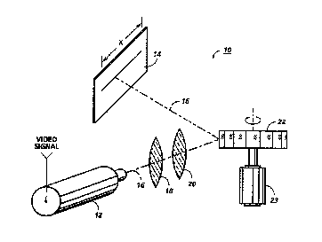
Figure 3 shows an imaging system 10 wherein a laser 12 produces a
coherent output which is scanned across photoreceptor 14. In response to
video signal information representing the information to be printed or
copied, the laser diode is driven so as to provide a modulated light output
beam 16. Flat field collector and objective lens 18 and 20, respectively,
are 3
-3-
~B
2 ~ .,.b
~- positioned in the optical path between laser 12 and
light beam reflecting scanning device 22. In a
preferred embodiment, device 22 is a multi-faceted
mirror polygon driven by motor 23, as shown. Flat field
collector lens 18 collimates the diverging light beam 16
and field objective
- 3a -
.,
¢
lens 20 causes the collected beam to be focused onto photoreceptor 14
after reflection from polygon 22. Photoreceptor 14, in a preferred
embodiment, is a layered photoreceptor shown in partial cross-section in
Figure 4.
Referring to Figure 4, photoreceptor 14 is a layered
photoreceptor which includes a conductive ground plane 32 formed on a
dielectric substrate 34 (typically polyethylene terephthalate (PET)), anti-
reflection layer 36, a blocking layer 38, interface layer 40, a charge
generating layer 42, and a transparent charge transport layer 44.
According to the present invention, anti-reflection coating 36 is formed
over the ground plane. A photoreceptor of this type (absent the anti-
reflection layer 36) is disclosed in U.S. Patent 4,588,667.
Photoreceptor 14 is subject to both the plywooding effect
problem described above as well as the delamination problem, also
described above. As will be seen, the thickness of the anti-reflection
coating 36 can be selected so as to address either or both problems.
Turning now to a more detailed consideration of anti-reflection
layer 36 shown in Figure 4, according to a first aspect of this invention, the
layer is designed to suppress the reflectivity of the light beams shown in
dotted form in Figure 1 from the surface of ground plane 32. The layer is
formed by means of neon RF sputtering, Q-beam evaporation or other
coating methods which allow deposition of the TiO2 on the ground plane
Layer 36 increases optical transmission through the ground plane thus
decreasing its reflectivity. It has been found that the interference fringe
contrast decreases as the index of the refraction of layer 36 increases, and
that materials with index of refractions of approximately 2.05 or greater
are most suitable for use as anti-reflection layers. This is demonstrated by
referring to Figure 5 which shows a plot of three different materials used as
anti-reflection layer 36. The plot shows total absorption plotted against
transport layer thickness. The coatings shown are of three different
materials (MgO~ Zr~2, TiO2) as well as a sample plot of absorption in the
absence of any anti-reflection coating. The thicknesses of each material
_ 2044340
used as anti-reflection coatings are optimized to produce the lowest
reflectivity at the layer 36 surface for a specific wavelength. The
modulation in the absorption correlates directly to the interference fringe
contrast with larger magnitude modulations signifying strong plywood
fringe contrast in the final output print. Conversely, a small magnitude
modulation results in weak plywood fringe contrast in the output print.
Thus, TjO2, with an index of 2.5 is a more preferable material than Zr~2
with an index of 2.05 which in turn is preferable to MgO with an index of
1.72. For comparison purposes, a plot of modulation with no anti-
reflection coating at all is shown to be quite close to the MgO plot. Other
acceptable anti-reflection materials are Cr2O3 with an Index=2.4.
Calculations for a photoreceptor of the type shown in Figure 4 with a
charge generator layer thickness of 1.8 microns and in the absence of an
anti-reflection layer results in a modulation of approximately 14%. The
modulation for a device with a TiO2 anti-reflection layer about 60 nm thick
reduces the modulation to 2.5% . The reduction in plywood fringe contrast
itself is greater then 5X.
According to a second aspect of the invention, it has been found
that if TiO2 is the material used for layer 36 and if the layer is formed to a
thickness of between 20nm and 180nm, the adhesion at the interface of
layers 42, 40 is greatly increased. The thickness may differ from the
optimum thickness stated above. The improvement was tested by
conducting a series of peel tests which measured reverse peel of adhesion
values at the interface of interest. As shown in Table 1, layer TiO2 layers of
various thicknesses were applied to a titanium ground plane in a
photoreceptor of the type shown in Figure 4. Adhesion values were
measured and compared to a control photoreceptor which measured the
adhesion without layer 36. As shown, the reverse peel strength was
improved by a factor of 7 or 8 times over the control. The optimum
thickness of the TiO2 ranges from 20nm to 180nm. In separate tests,
electrical parameters of the photoreceptor such as dark decay sensitivity or
electrical cyclic stability were not affected.
X044340
Table 1 Adhesion Values of TiO2
Sample Reverse Peel
Description
comments
(nm) observation) peeli g
Ti 44.1 42/40 non-
uniform
Ti 38.6 42/40 non-
90.6 uniform
120 Ti 51.9 U/40: non-
uniform
180 Ti 45.7 42/40 non- .
uniform
control Ti 6.7 42/40 uniform -
(mod 5,
web)
While the invention has been described with reference to the
structure disclosed, it will be appreciated that numerous changes and
modifications are likely to occur to those skilled in the art, and it is intended
to cover all changes and modifications which fall within the true spirit and
scope of the invention.