Note : Les descriptions sont présentées dans la langue officielle dans laquelle elles ont été soumises.
20~4426
.~
INFORMATION RECORDING AND REPRODUCING DEVICE
FIELD OF THE INVENTION
The present invention relates to an information
recording and reproducing device which records and
reproduces information on disk-shaped recording media such
as optical disks.
BACKGROUND OF THE lNV~N'l'ION
With an optical disk recording and reproducing
device, each track on an optical disk is divided into a
plurality of sectors, and information is
recorded/reproduced on the disk sector by sector. Here,
header information, such as a sector mark and address
information, is recorded in each sector. The sector mark
indicates a reference position of a sector and the address
information the address of a sector.
- 2 - 204442G
.~
The address of a sector being scanned by an optical
beam is identified by reproducing the header information.
This operation also enables access to the address of a
desired sector.
Among recording methods for the optical disk
recording and reproducing device, the following two
methods, i.e. CAV (Constant Angular Velocity) method and
CLV (Constant Linear Velocity) method, are well known and
widely adopted. In the CAV method, data is
recorded/reproduced on an optical disk in accordance with
a recoding and reproduction use clock signal with a
predetermined frequency while rotating the disk at a
constant angular velocity. In CLV method, information is
recorded/reproduced on an optical disk in accordance with
a recoding and reproduction use clock signal with a
predetermined frequency while rotating the disk at a
constant linear velocity.
In the CAV method, while a recording density in an
outer portion of a disk is lower than a recording density
in an inner portion thereof, high-speed access to a
desired sector is achieved. On the contrary, in the CLV
method, high recording capacity is achieved as the linear
recording density is constant from an inner portion to an
outer portion of a disk. However, the rotating speed of
the disk is controlled to keep a constant linear velocity,
204442~
thereby resulting in slow access to a desired sector.
Thus, the both methods have merits and demerits.
To counteract this, MCAV (Modified Constant Angular
Velocity) method, which achieves an increased recording
capacity of an optical disk and high-speed access to a
desired sector, is suggested and put into practice. In
this method, the optical disk is rotated at a constant
angular velocity, and the recording area of the disk is
divided into a plurality of ring-shaped zones of
concentric circles so that recording and reproduction use
clock signals have frequencies which increase from the
innermost zone outwards.
As for access to a desired sector in an optical disk
recording and reproducing device using the MCAV method, an
optical beam is moved to a track belonging to the desired
sector in a radial direction of the disk while stopping
tracking control, and then tracking control is executed
again.
At this time, if a sector being scanned by the
optical beam belongs to a different zone from the desired
zone whereto the desired sector belongs, the frequency of
the recording and reproduction use clock signal needs to
be changed to correspond to the zone by a process of trial
and error in order to reproduce the header information in
each sector in a track. Therefore, access time increases.
~ 4 ~ 2044~26
When the optical beam moves to a track in a different
zone due to a tacking control failure caused by for
example some defects on the optical disk, the access time
also increases.
SU~MARY OF THE INVENTION
An object of the present invention is to increase a
recording capacity of an optical disk and to achieve
high-speed access to a desired sector.
In order to achieve the object, an information
recording and reproducing device according to the present
invention divides a recording area of an optical disk into
a plurality of ring-shaped zones of concentric circles,
arranges the number of sectors composing one track to be
uniform in each zone and the number of sectors to increase
from inside towards an outermost zone, rotates a
disk-shaped recording medium, which is provided with a
header area in each sector wherein header information such
as address information is recorded and a data area wherein
data is recorded, at a constant angular velocity, and
records/reproduces data in the data area by using clock
signals whose frequencies increase from the innermost zone
towards the outermost zone.
More specifically, the present invention uses the
disk-shaped recording medium whereon the header
_ 5 _ 2044426
information is recorded in accordance with a clock signal
with a fixed frequency, and comprises: a first clock
generating circuit for generating a first clock signal
corresponding to the clock signal of the fixed frequency;
a second clock generating circuit for generating a second
clock signal corresponding to clock signals whose
frequencies for recording and reproducing data vary in
each zone; a header information reproducing circuit for
reproducing the header information in accordance with the
first clock signal; and a control circuit for controlling
the frequency of the second clock signal according to
reproduced header information.
In this arrangement, during access to an arbitrary
sector, the header information can be accurately
reproduced in accordance with the first clock signal
having the fixed frequency irrelevant to any zone.
Consequently, according to the obtained header
information, data can be immediately recorded and
reproduced by switching a frequency of the second clock
signal to a frequency assigned for a zone to which the
sector belongs, which allows the access time to be
shortened. Moreover, as the data is recorded and
reproduced by employing the MCAV method, a recording
capacity of the disk-shaped recording medium can be
increased.
- 6 - 2044426
For a fuller understanding of the nature and
advantages of the invention, reference should be made to
the ensuing detailed description taken in conjunction with
the accompanying drawings.
BRIEF DESCRIPTION OF THE DRAWINGS
Fig. 1 to Fig. 7 shows one embodiment of the present
invention.
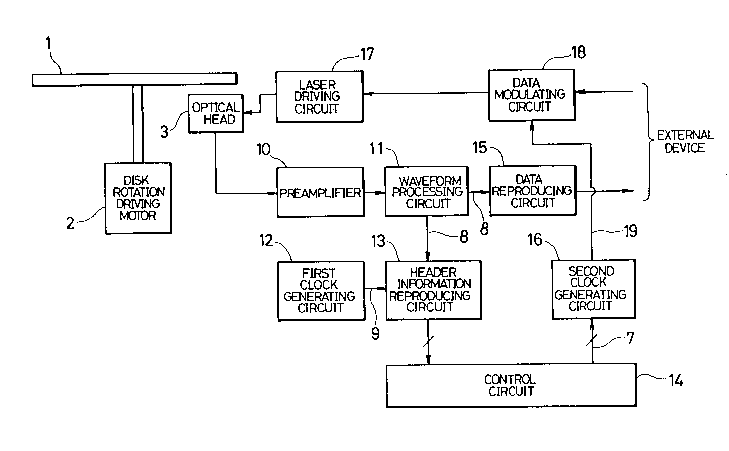
- Fig. 1 is a block diagram schematically illustrating
the structure of an optical disk recording and reproducing
device.
Fig. 2 is a block diagram illustrating a concrete
example of a header information reproducing circuit.
Fig. 3 is a block diagram illustrating a concrete
example of a second clock generating circuit.
Fig. 4 is a block diagram illustrating another
concrete example of the second clock generating device.
Fig. 5 is an explanatory view illustrating the
allocation of zones on an optical disk used with an
information recording and reproducing device of the
present invention.
Fig. 6 is an explanatory view illustrating a header
area and a data area on a track in each zone.
Fig. 7 is an explanatory view illustrating a format
of header information.
_ 7 _ 2044426
DESCRIPTION OF THE EMBODIMENTS
Referring to Fig. 1 to Fig. 7, the following will
explain an optical disk recording and reproducing device
as an embodiment of the present invention.
First, an optical disk as a disk-shaped recording
medium used in the optical disk recording and reproducing
device of this embodiment will be discussed below.
A recording area on the optical disk is divided into
a plurality of ring-shaped zones of concentric circles.
More specifically, as shown in Fig. 5, for example an
optical disk 1 with 130 mm-diameter is divided into five
zones, la to le. Each zone has 3750 tracks, and therefore
the optical disk 1 totally has 18750 tracks.
Fig. 6 shows the allocation of a header area 4 and a
data area 5 on the tracks. Here, (a) to (e) of the figure
show allocations with respect to the tracks in the zones
la to le, and the horizontal axis indicates the sizes of
the areas by an index of time.
The header area 4 and the data area 5 are
respectively 52-byte and 1274-byte in length. One sector
is composed of the header area 4, the data area 5 and a
gap 6 therebetween.
The number of sectors per track increases from the
innermost zone la towards the outermost zone le. More
specifically, the numbers of sectors per track in the
- 8 - 2044426
zones la to le are 17, 20, 23, 26 and 29, respectively.
This corresponds with the length of a sector on a
time base which decreases from the innermost zone la
towards the outermost zone le as shown by (a) to (e) of
Fig. (6). This is based on the fact that the frequencies
of the record and reproduction use crock signals need to
be increased from the innermost zone la towards the
outermost zone le in order to improve the recording
capacity.
In the mean time, in this embodiment, the
reproduction of the header area 4 is executed in
accordance with the clock signal of the fixed frequency
irrelevant to any zone, and therefore the length of the
header area 4 on a time base is constant in every zone as
shown in (a) to (e) of Fig. 6.
For example, when the optical disk 1 (see Fig. 5) is
rotated at a constant angular velocity (e.g. 1800
rotations per minute) and (2, 7) run length limiting code
is used as a recording code, data is recorded/reproduced
in the data area 5 in accordance with a clock signal of a
frequency of 11.0976 MHz in the zone la, 13.1482 MHz in
the zone lb, 15.2281 MHz in the zone lc, 17.3377 MHz in
the zone ld, and 19.4778 MHz in the zone le.
Information is reproduced from the header area 4 in
accordance with a clock signal of a frequency of, for
9 20~44~6
.
example, 11.0976 MHZ. The frequency used here is arranged
to be equal to the frequency for recording and reproducing
data in the data area 5 in the zone la, and it is constant
in every zone as aforesaid.
For a format of the header information in the header
area 4, as shown in Fig. 7 it comprises a sector mark (SM)
indicating a leading position of a sector, a pattern (VFO)
for pulling into synchronization, an address mark (AM)
indicating the location of address information, the
address information of the sector (ID), VFO, AM, ID, VFO,
AM, ID, and a postamble (PA) for stably reproducing the
last ID, in this order.
Regarding a recording code for the sector mark (SM),
generally, in order to discriminate it from the recording
code for the data area 5 (Fig. 6), a group of patterns
whose length can never be produced by any combination of
data patterns is used. The sector mark ( SM) is recorded
by the use of a special mark created by rows of these
patterns. On the contrary, the same recording code as the
data area 5 is used for the address information ( ID).
In this configuration, the recording area of the
optical disk 1 is divided into a plurality of zones, la to
le, of concentric circles (see Fig. 5) and the frequency
of the recording and reproduction use clock signal is
increased from the innermost zone la towards the outermost
2044426
zone le in the data area 5 (see Fig. 6), which allows the
length, with respect to time base, of each sector in outer
portions to be decreased and the recording capacity to be
increased. Moreover, as the header information can be
reproduced in accordance with the clock signal of the
fixed frequency, the header information is always
available during the tracking control.
Consequently, even when accessing to a sector which
belongs to a zone different from a sector being accessed,
the access action during recording/reproduction can be
immediately performed according to the address information
(ID) reproduced in accordance with the clock signal of the
fixed frequency, thereby shortening the access time.
The optical disk recording and reproducing device
(information recording and reproducing device) according
to the present invention uses the optical disk 1. As
shown in Fig. 1, the device is composed mainly of a disk
rotation driving motor 2, an optical head 3, a laser
driving circuit 17, a data modulating circuit 18, a
preamplifier 10, a waveform processing circuit 11, data
reproducing circuit 15, a first clock generating circuit
12, a header information reproducing circuit 13, a control
circuit 14, and a second clock generating circuit 16. The
disk rotation driving motor 2 drives the optical disk 1 to
rotate. The optical head 3 records information by
11 2044426
irradiating laser light and reproduces information by
detecting reflected light. The laser driving circuit 17
supplies a laser driving current to the optical head 3.
The data modulating circuit 18 modulates recording data in
accordance with a second clock signal lg and sends the
resulting output to the laser driving circuit 17. The
preamplifier 10 amplifies a signal detected by the optical
head 3. The waveform processing circuit 11 converts an
output signal of the preamplifier 10 into a binary signal.
The data reproducing circuit 15 demodulates data from a
binary signal 8 (reproduced digital signal) which is
released from the waveform processing circuit 11. The
first clock generating circuit 12 generates a first clock
signal 9 of a frequency for reproducing the header
information. The header information reproducing circuit
13 reproduces the header information from the binary
signal 8 which is released from the waveform processing
circuit 11 in accordance with the first clock signal 9.
The control circuit 14 sends a control signal 7 to the
second clock generating circuit 16. The control signal 7
switches a frequency of the second clock signal 19 into a
frequency corresponding to one of the zones la to le,
according to the address information (ID) released from
the header information reproducing circuit 13. According
to the control signal 7 from the control circuit 14, the
- 12 - 2044426
.
second clock generating circuit 16 outputs the second
clock signal 19 having an assigned frequency for recording
data.
In the above configuration, the optical disk 1 is
driven by the disk rotation driving motor 2 such that it
rotates at a constant angular velocity. In this
embodiment, the disk 1 rotates at a constant angular
velocity (e.g. 1800 rotations per minute).
During recording, recording data from an external
device (not shown) is input to the data modulating circuit
18 and modulated into a form of, for example, (2, 7) run
length limiting code.
According to the second clock signal 19 of the
assigned frequency which is released from the second clock
generating circuit 16, the modulated data is sent to the
laser driving circuit 17. The laser driving circuit 17
supplies a laser driving current, which varies according
to the input modulated data, to the optical head 3.
According to the laser driving current, the amount of
light irradiated on the optical disk 1 from the optical
head 3 is controlled, and the information is recorded in
the data area 5 by the so-called light modulating method.
For example, in case of the optical disk 1 with
perforated pits, when a light beam of strong intensity is
irradiated on the disk, the temperature of the portion
- 13 - 2044426
whereon the light beam is irradiated rises and a pit as a
recording bit is formed on the recording medium, whereby
information is recorded.
Meanwhile, during reproduction, a light beam with a
constant intensity is irradiated on the optical disk 1
from the optical head 3. The amount of the light beam is
such small that it does not make a recording bit on the
disk 1. Reflected light corresponding to the recorded
information is detected by the optical head 3, converted
into an electric signal, and sent to the preamplifier 10
where the signal is amplified at a predetermined
amplification factor.
An output of the preamplifier lO is sent to the
waveform processing circuit 11 where it is filtered and
converted into a binary signal, and then the resulting
binary signal 8 is respectively sent to the data
reproducing circuit 15 and the header information
reproducing circuit 13.
In the data reproducing circuit 15, data is
demodulated from the signal 8 in accordance with a clock
signal, and the demodulated data is then sent as
reproduced data to the external device. The clock signal
has a frequency substantially equal the frequency of the
second clock signal 19 from the second clock generating
circuit 16.
~ 14 _ 2044426
Meanwhile, in the header information reproducing
circuit 13, header information is reproduced from the
binary signal 8 in accordance with the first clock signal
9 of the fixed frequency output from the first clock
generating circuit 12. In other words, by detecting a
sector mark (SM), a leading position of a sector is
determined, and address information (ID) is reproduced and
sent to the control circuit 14.
More specifically, as shown in Fig. 2, the header
information reproducing circuit 13 comprises, for example,
a pattern detecting circuit 20, a majority logic circuit
21, a timing generating circuit 22, and an address
information reproducing circuit 23. The pattern detecting
circuit 20 detects a pattern used for a sector mark (SM)
from the binary signal 8 released from the waveform
processing circuit 11, and outputs the resulting detected
pulses. The majority logic circuit 21 detects the sector
mark by counting the detected pulses, and outputs sector
mark detection pulses. According to the sector mark
detection pulses, the timing generating circuit 22 outputs
timing pulses for reproducing the address information
(ID). According to the timing pulses, the address
information reproducing circuit 23 reproduces the address
information (ID) from the binary signal 8 released from
the waveform processing circuit 11, and outputs it to the
- 15 _ 2044426
control circuit.
With the configuration of the header information
reproducing circuit 13, according to the number of clock
pulses of the first clock signal 9 which is counted
between the pulse edges of the binary signal 8, the
pattern of the sector mark (SM) is detected in the pattern
detecting circuit 20, and the detected pulses are then
sent to the majority logic circuit 21.
In the majority logic circuit 21, the input detected
pulses are counted, and if they exceed a preset number,
they are verified as the sector mark (SM). Namely, the
detection of the sector mark is executed according to the
so-called majority logic.
In the timing generating circuit 22, according to the
sector mark detection pulses from the majority logic
circuit 21, the timing pulses for reproducing the address
information (ID) are generated. In the address
information reproducing circuit 23, according to the
timing pulses, the address information (ID) is reproduced
from the binary signal 8 and then sent to the control
circuit 14.
- As aforesaid, according to the control signal 7 from
the control circuit 14, the second clock generating
circuit 16 (see Fig. 1) outputs the second clock signal 19
of an assigned frequency for recording data. More
- 16 - 2044426
precisely, as shown in Fig. 3, the second clock generating
circuit 16, for example, comprises quartz oscillators 24a
to 24 e and a selecting circuit 25 which selects one
oscillator from the quartz oscillators 24a to : 24e
according to the control signal 7 from the control circuit
14 and outputs it.
Nith the configuration of the second clock generating
circuit 16, the oscillation frequencies of the quartz
oscillators 24a to 24e respectively correspond to the
frequencies of the recording and reproduction use clock
signals for five zones la to le of the optical disk 1 (see
Fig. S), and signals of five different frequencies are
input to the selecting circuit 25.
In the selecting circuit 25, according to the control
signal 7 from the control circuit 14, one of clock signals
whose frequencies for recording and reproduction
correspond to the respective zones, la to le,-is selected
and released as the second clock signal l9 to the data
modulating circuit 18.
As aforesaid, the device in this embodiment has two
separate clock generating circuits, i.e. the first clock
generating circuit 12 (see Fig. l) and the second clock
generating circuit 16. However, the present invention is
not restricted to this configuration. For instance, when
the reproduction of the header information and the
- 17 _ 2044426
recording/reproduction in the zone la are e~ecuted in
accordance with clock signals of the same frequency like
the optical disk 1, the quartz oscillating circuit 24a can
serve as the first clock generating circuit 12, and
therefore the number of parts can be decreased.
Moreover, the quartz oscillators 24a to 24e are used
as the second clock generating circuit 16 in Fig. 3.
However, the present invention is not restricted to this
concrete configuration, and for example, a PLL (Phase
Locked Loop) may be used as shown in Fig. 4.
In this case, the second clock generating circuit 16
comprises a reference clock generating circuit 26, a
programmable frequency divider 27, a phase comparator 28,
a phase/voltage converter 29, a voltage controlled
oscillator 30, and a programmable frequency divider 31.
The reference clock generating circuit 26 generates a
reference clock. The programmable frequency-divider 27
reduces the frequency of the reference clock by a dividing
factor which varies according to the control signal 7 from
the control circuit 14. The phase comparator 28 compares
a phase of an output of the programmable frequency divider
27 with that of the programmable frequency divider 31 and
detects a difference between the phases. The
phase/voltage converter 29 converts the detected
difference into voltage accordingly. The voltage
- 18 -
"- 204~426
controlled oscillator 30 generates a clock signal of a
frequency which varies according to an output voltage from
the phase/voltage converter 29. The programmable
frequency divider 31 reduces the frequency of clock signal
from the voltage controlled oscillator 30 by a dividing
factor which varies according to the control signal 7 from
the control circuit 14 (see Fig. 1).
With the configuration of the second clock generating
circuit 16, the dividing factor of the programmable
frequency divider 27 is controlled by the control signal 7
from the control circuit 14. In other words, the
frequency of the reference clock signal from the reference
clock generating circuit 26 is reduced by the dividing
factor. The resulting clock signal having the reduced
frequency is sent to the phase comparator 28.
In the mean time, an output of the voltage controlled
oscillator 30 is sent to the programmable frequency
divider 31 where its frequency is reduced by the dividing
factor which varies according to the control signal 7 from
the control circuit 14, and then sent to the phase
comparator 28.
In the phase comparator 28, phases of the signals
sent from the programmable frequency divider 27 and the
programmable frequency divider 31 are compared with each
other, and a detected phase difference between the phases
2044426
is sent to the phase/voltage converter 29. In the
phase/voltage converter 29, the detected difference is
converted into voltage which also varies accordingly, and
is then sent to the voltage controlled oscillator 30.
By executing PLL control, information is
recorded/reproduced in the zones la to le in accordance
with the second clock signal 19 that is a clock signal
having the frequency reduced by the programmable frequency
divider 27.
For example, when the frequency of the reference
clock signal is set at 11.0976 MHz (using a clock signal
of this frequency, information is recorded/reproduced in
the zone la (see Fig. 5)) and a dividing factor M of the
programmable frequency divider 27 and a dividing factor N
of the programmable frequency divider 31 are respectively
set at 92 and 109, the second clock signal 19 from the
voltage controlled oscillator 30 has a frequency of
13.1482 MHz (using a clock signal of this frequency,
information is recorded/reproduced in the zone lb (see
Fig. 5)).
Similarly, when the dividing factors (M and N) of the
frequency dividers 27 and 31 are respectively set at 43
and 59, the second clock signal 19 from the voltage
controlled oscillator 30 has a frequency of 15.2269 MHz
(using a clock signal of this frequency, information is
2044~26
recorded/reproduced in the zone lc (see Fig. 5)).
When the dividing factors (M and N) of the
programmable frequency dividers 27 and 31 are respectively
set at 16 and 25, the second clock signal 19 from the
voltage controlled oscillator 30 has a frequency of
17.3400 MHz (using a clock signal of this frequency,
information is recorded/reproduced in the zone ld (see
Fig. 5))-
When the dividing factors (M and N) of theprogrammable frequency dividers 27 and 31 are respectively
set at 49 and 86, the second clock signal 19 from the
voltage controlled oscillator 30 has a frequency of
19.4774 MHz (using a clock signal of this frequency,
information is recorded/reproduced in the zone le (see
Fig. 5)).
While the second clock signal 19 may have a frequency
which is slightly different from the assigned frequency of
the recording and reproduction use clock signal, the
difference can be easily compensated by providing safety
margins for the entire optical disk recording and
reproducing device, for example giving the gaps 6 to the
respective sectors (see Fig. 6), and therefore this is not
a serious problem.
As aforesaid, when the second clock generating
circuit 16 is composed of the PLL, the frequency of the
2044426
second clock signal 19 can be varied by changing the
combination of the dividing factors (M and N) of the
programmable frequency dividers 27 and 31. Therefore,
even when the number of zones arranged on the optical disk
1 is greater than the present five zones la to le, there
is no need for increasing the number of parts.
The numeric values used for specifying the number of
zones on the optical disk 1, the number of sectors per
track and other numbers are just examples, and therefore
this invention is not restricted to these values.
In this embodiment, an optical disk recording and
reproducing device is explained, however the same may be
applicable to optical disk reproducing devices.
As for the optical disk 1, a read only optical disk
such as a compact disk, a write once optical disk of
etching type, and an erasable optical disk such as a
magneto-optical disk may be used.
As aforesaid, the information recording and
reproducing device of the present invention uses the disk
type recording medium whereon the header information is
recorded in accordance with the clock signal of the fixed
frequency, and comprises: the first clock generating
circuit for generating the first clock signal
corresponding to the clock signal of the fixed frequency,
the second clock generating circuit for generating the
- 22 - 204~426
second clock signal corresponding to the clock signals
whose frequencies for recording and reproduction vary in
each zone; the header information reproducing circuit for
reproducing the header information in accordance with the
first clock signal; and the control circuit for
controlling the frequency of the second clock signal
according to the reproduced header information.
Thus, during access to an arbitrary sector, the
header information can be accurately reproduced in
accordance with the first clock signal of the fixed
frequency irrelevant to any zone. Consequently, according
to the obtained header information, data can be
imme~iately recorded/reproduced by switching a frequency
of the second clock signal to a frequency assigned for a
zone whereto the sector belongs, thereby resulting in a
significant decrease in the access time.
Besides, even when a sector in a different zone is
accessed due to tracking control failure caused by some
disk defects, information on the header area can be
reproduced in accordance with the clock signal of the
fixed frequency in the same manner as above, and therefore
the access time can never be increased.
The invention being thus described, it will be
obvious that the same may be varied in many ways. Such
variations are not to be regarded as a departure from the
204442~
spirit and scope of the invention, and all such
modifications as would be obvious to one skilled in the
art are intended to be included within the scope of the
following claims. -