Note : Les descriptions sont présentées dans la langue officielle dans laquelle elles ont été soumises.
6~768-246
2045880
DEVICE OP~RABLE WITH
AN EXCELLENT SPECTRUM SUPPRESSION
Background of the Inventlon:
This invention relates to a device for use in
processing a baseband input signal and a carrier signal
into an envelope output signal and, more partlcularly, to
5 an improvement in spectrum suppresslon under a burst
switching condition used in a TDMA type radio
communication apparatus ln which a modulated signal has
- an envelope.
In general, a device of the type descrlbed is
10 supplied with a baseband input signal and a carrier
signal to produce an envelope output signal.
The device comprises a modulating unlt responsive
to the baseband input signal and the carrier signal for
producing a modulated signal variable within a power
15 range. A waveform generating unit is supplied with a
burst control signal and generates a control signal for
controlling the power range 1nto a controlled region. An
amplifying unit is connected to the modulating unit and
- 2045880
the waveform generating unlt and amplifies the modulated
signal having the contrslled reglon to make the envelope
output signal represent an envelope of the modulated
signal and to produce the envelope output signal.
A conventional device is dlsclosed in United
States Patent No. 4,592,073 issued to Kyoji Watanabe and
assigned to NEC Corporation. According ~o Wa~anabe
patent, the device comprlses a waveform generating unit
for receiving the burst con~rol signal having a
rectangular waveform and for generating ~he con~rol
I (~
signal for controlling the power range into the
controlled region. The control slgnal has a controlled
shape comprising sloping leading and tralling edges and a
plateau between the sloping leadlng and trailing edges.
The modulating unit always modulates Lhe baseband input
signal and the carrier signal into the modulating signal
with no consideration given to the burst control signal.
The amplifying unit amplifies the modulatlng signal
having the controlled region to make the envelope output
signal represent the envelope of the modulatlng signal.
2U
As a result, the envelope output signal has a shape which
is similar to the controlled shape. Therefore, the
modulated signal is amplified throughou~ the sloping
leading and traillng edges and the plateau.
However, it has now been found by the present
~5
lnventor that it is impossible Lo suppress a spectrum
divergence of the enveiope output signal within a
predetermined guard mask which lS a permitted limit of
2045880
the spectrum divergence in the envelope output signal.
When the spectrum divergence overrun the guard mask, a
jamming occurs as a result of the envelope output signal.
Therefore, a transmission interference occurs. This is
because the modulated signal inevltably has an lnherent
band. Even if the ampl ifylng unlt ~rle~ to ampllfy the
modulated signal in due consideratlon of the inherent
band in order to avoid such a trouble, a very delicate
adjustment is required in the amplifying unit.
Sur~mary of the Invention;
1~
It is therefore an object of the present
invention to provide a device for improving a spectrum
suppression under a burst switching conditlon.
It is another object of this invention to provide
a device of the type described, which can suppress a
spectrum divergence withln a predetermined guard mask.
It is still another object of this invention to
provide a device of the type described, whlch can
suppress a spectrum divergence Wittl no need for delicate
adjustment.
2()
On describlng the gist of an aspect of this
invention, it is possible to understand that a device is
for use in processing a baseband input signal and a
carrier signal into an envelope output signal. The
device comprises producing means responslve to the
baseband input signal and the carrier signal for
producing a produced signal variable having a power
range. Responsive to a burst control signal, waveform
2045880
generating means generates a control signal for
controlling the power range into a controlled region.
Amplifylng means is connected to the producing means and
the waveform generating means and ampl.lfies the produced
signal having the controlled region to make said envelope
output signal represent an envelope of the produced
si.gnal and ~o produce the envelo~e ou~pu~ nal.
According to this aspect of the invention, the
producing means comprises modulating means for modulating
the baseband input signal and the carrler aignal into the
J~
produced signal, and switching means supplied with the
burst control signal for switching on and off the
modulating means to produce a modulated signal and a
non-modulated signal one at a time as the produced signal
having the controlled region.
I ~
On describing the gist of another aspect of this
invention, it is possi.ble to understand that a device
which is for use i.n processi.ng a baseband input signal
and a carrier signal into an envelope output signal. The
devi.ce comprises producing means responsive to ~he
baseband input signal and the carri.er signal for
producing a produced signal variable having a power
range. Waveform generating means responslve to a burst
control signal generates a control signal for controlling
the power range into a controlled region. Amplifying
means is connected to the producing mean~ and the
waveform generating means and amplifies the produced
signal having the controlled region to make the envelope
- Z045880
output signal represent an envelope of the produced
signal and to produce the envelope output 6ignal.
According to this aspect of the invention, the
producing means comprises modulating means for modulating
the baseband input signal and the carrier signal into the
produced signal, and switching means supplied with the
control ~ignal for ~wltchlng on and off L~o ~odul~lng
means to produce a modulated signal and a non-modulated
signal one at a time as the produced signal having the
controlled region.
1 0
Brief Description of the Drawlngs;
Fig. 1 is a block diagram of a device according
to a first embodiment of the instant invention;
Fig. 2(a) shows one e~ample of a burst control
signal which is used in the device illusLrated in Fig. 1
I ~
and has a rectangular waveform;
Fig. 2(b) show6 one exanlple of a control signal
which i6 used in the device illustrated in Fig. 1 and has
a controlled shape comprising sloping leading and
trailing edges and the plateau between the leading and
21)
trailing edges;
, Fig. 2(c) shows an envelope of a produced signal
which is used in the device illustrated in Fig. l;
Fig. 2(d) is a time chart of modulation by a
switching unit which is used in the device illubtrated in
Fig. l;
Fig. 3(a) is a graph illustrative of a line
spectrum of a non-modulated signal;
204S880
Fig. 3(b) is a graph showing the spectrum
divergence of the modulated signal; and
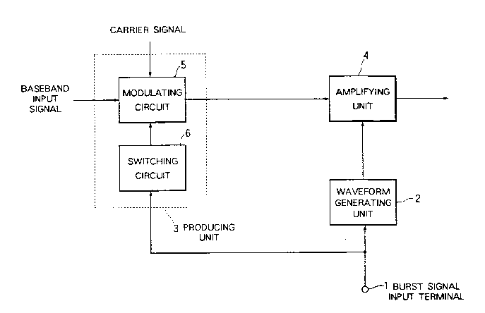
Fig. 4 is a block diagram of a device according
to a second embodiment of the instant invention.
Description of the Preferred Embodiments:
A device in accordance with the present invention
i~ supplied with a bdseb~n~ inpu~ ~lgnal ~nd ~ c~rr~r
signal and produces an envelope output signal.
Referring to Fig. 1, the device comprises a
producing unit 3 for producing a produced slgnal variable
I ()
having a power range according to a first embodiment of
this invention. A waveform generatiny unlt 2 is for
generating a contro~ signal for controlllng the power
range into a controlled region. An amplifying unlt 4 is
for amplifying the produced signal having a controlled
region.
The producing unit 3 includes a modulating
circuit 5 and a switching circuit 6. The modulating
circuit 5 is for modulating the baseband signal and the
carrier signal into the produced signal. The switching
2()
circuit 6 is supplied with a burst control signal from a
burst control signal input terminal 1 and ~witches on and
off the modulating circuit 5 to produce a modulated
signal and a non-modulated signal one at a time as the
produced signal. The waveform generating unit 2 is
supplied with the burst control signa~ from the burst
control signal input terminal 1 and generates the control
signal for controlling the power range into the
2045880
controlled region.
Referring to Flgs. 2(a) and (b~, the bur~t
control signal has a shape comprising a rectangular
waveform which ha~ an inherent characteristic and is
shown in Fig. 2(a). The waveform generating unit 2
generates the control slgnal having a controlled shape
from the burst control signal, as shown in Fig. 2(b).
The controlled shape comprises sloping l,eading
and trailing edges and a plateau between the leading and
trailing edges. Each of the sloping leading and tralling
I û
edges has a sloping time interval. The plateau has a
plateau time interval.
The sloping time and the plateau time interval
can be predetermined from the inherent characteristic of
the burst control signal.
Returning to Figs. 1 and 2(c) and ~d), the
switching circuit 6 is for switching off the modulating
unit 5 during each of the sloplng time interval to
produce the non-modulated signal and is to switch on
during the plateau time interval to produce the modulated
~0
signal, as shown in Fig. 2(d).
The amplifying unit 4 is connected to the
producing unit 3 and the waveform generating unit 2 and
amplifies the produced signal having the controlled
region to make the envelope ou~put signal repre~ent an
envelope of the produced signal and to produce ~he
envelope output signal, as shown in Fig. 2(c). In this
event, when the switching circuit 6 switches off the
204~880
modulating unit 3 to produce the non-modulated signal.
Figs. 1 and 3(a) will be referred to. The
amplifying unit 4 amplifies the non-modulated signal to
produce the envelope output signal having line spectrum,
as shown in Fig. 3(a). On the other hand, when the
switching circuit 6 switches on the modulating unit 3 to
produce the modulated signal, the amplifying unit 4
amplifies the modulated signal to produce the envelope
output signal having spectrum divergence, as shown in
Fig. 3(b).
I ()
In Fig. 2(c), the envelope output signal could
have the line spectrum at the sloplng leading and
Lrailing edges and the spectrum divergence at the
plateau. Therefore, it is possible to suppress the
spectrum divergence to be within a predetermined guard
I ~
mask which is a permitted limit of the spectrum
divergence. This is because the line spectrum of the
envelope output signal corresponds to the leading and
trailing edges.
Referring to Fig. 4, the description will be made
~()
as regards a case where the first switching circuit 6 is
supplied with the control signal instead of the burst
control signal according to a second embodiment of this
invention. The waveform generating unit 2 is connected
to the switching circuit 6 and generates the control
signal. The control signal comprises a sloping signal
and a plateau signal collectively representative of the
controlled shape.
204`5880
In the manner depicted in Fig. 2(b), the sloping
fiignal reprefient~ the sloping leading and trailing edgefi.
The plateau slgnal representfi the plateau between the
sloping leading and trailing edges.
Returning to Fig. 4, the switching circuit 6 ifi
to fiwitch off the modulating circuit 5 in refiponse to the
sloping signal to produce the non-modulated signal and is
to fiwitch on in response to the plateau fiignal to produce
the modulated fiignal in the same manner of the above
deficription .
1()