Note : Les descriptions sont présentées dans la langue officielle dans laquelle elles ont été soumises.
~ 2~460~9
1 BACKGROUND OF THE INVENTION
The invention relates to a video signal
processing apparatus in an image display apparatus which
can display a video image having a different aspect ratio
onto a screen or a cathode ray tube (hereinafter,
abbreviated to a CRT) of a wide aspect of 9: 16 of a
high definition television receiver, a video projection
system (hereinafter, abbreviated to a VPS), or the like.
When a video image having such a different aspect ratio
is displayed, the invention enables such a video image
to be displayed as large as possible.
In recent years, as the number of video
softwares, particularly, softwares of movies has been
increased, the number of softwares of the vista size or
cinema size also increases. If such a video software is
displayed onto the CRT having an aspect ratio of 3: 4
of the television receiver of the NTSC system, blanks
occur in the upper and lower portions of the screen.
The number of video images of the wide aspect ratio for
the high definition television receiver or the like will
increase in future. Therefore, an efficient display
method is being .~7rAm; n~
Fig. 1 is a schematic block diagram of a clear
vision (EDTV: Extended Definition Television) .
In the diagram, reference numeral 1 denotes
20460~9
1 a selector for selecting and outputting one of a
plurality of video sources Vl to V4; 2 an AGC circuit
to always keep an amplitude of a video (111min~n~e~ signal
constant; 3 a chroma demodulating circuit to demodulate
5 a chLI ;ni~n~e signal included in the video signal; 4 an
A/D converting circuit to analog-digital convert the
video (luminance) signal and the chL, in~nce signals;
5 a signal processing circuit to produce interpolation
signals which are necessary for the three-dimensional
10 Y/C separation, motion detection, and double-speed
sequential scan which are needed to the EDTV; 6 a memory
circuit to execute the double-speed sequential scan;
7 a PLL circuit to generate clocks for the A/D conversion
and clocks necessary for the double-speed sequential
15 scan; 8 a control circuit which receives an output of
the PLL circuit 7 and produces various kinds of control
signals; 9 a D/A converting circuit to convert a digital
video signal which has been converted into a double-speed
signal by the memory circuit 6 into an analog signal;
20 and 10 a matrix circuit to convert D/A converted
luminance signal (2Y) and chL- in~noe signals (2I, 2Q)
into primary color signals of R, G, and B.
The operation of the EDTV constructed as
mentioned above will now be l~riefly described herein-
25 below.
One of the video signals in the video sourceselected by the selector 1 is supplied as a lll~in;lnce
signal to the AGC circuit 2 and is subjected to the AGC
-- 2 --
2~G0~9
90 as to make an output amplitude constant and, there-
after, the signal is sent to the A/D converter 4. The
one of the video signals is supplied as a chrominance
signal (C signal) to the chroma ~ 1 Ating circuit 3
5 and is ~1 1 Ated into an I (R-Y) signal and a Q (B-Y)
signal. The I and Q signals are similarly sent to the
A/D converting circuit 4.
The one of the video signals is supplied as
a sync signal to the PLL circuit 7, by which the
10 oscillation is executed at a frequency of 28 . 6 MHz
(= 8fSC: fsc = 3-579545 MHz) as ~lln~ ntal clocks which
are necessary for the double-speed sequential scan,
thereby accomplishing the phase lock with a horizontal
sync signal.
The A/D converting circuit 4 quantizes and
converts the luminance signal into the digital signal
at 14.3 MHz (4fsc) on the basis oi~ 8 bits and 256
grA(lAt; ~n~ The A/D converting circuit 4 quantizes and
converts the C signal into the digital signal at 3 . 58
20 MHz (fsc) on the basis of 7 bits and 128 gradations.
The signal processing circuit 5 receives output signals
of the A/D converting circuit 4 and executes various
kinds of processes to realize a high picture quality and
produces interpolation signals which are necessary for
25 the three-dimensional Y/C separation, motion detection,
and double-speed sequential scan. In the above case,
the signal processing circuit 5 generates the lllm;nAne~
signal and the chl, ; nAn- e signal of the present line
-- 3 --
2Q46049
and the 11~--; n~n~e signal and the chl~ i n~nf e signal
of the interpolation line. The horizontal frequency
until the above stage is set to 15 . 75 kHz .
The memory circuit 6 is a circuit which is
5 n~ 5g; ry to execute the double-3peed sequential scan
by receiving the processes of the signal processing
circuit 4. The writing operation into the memory is
executed every scan (lH) by the clocks of 14.3 MHz. The
reading operation from the memory is performed at a
10 frequency of 28 . 6 MHz by alternately reading out data
from the present line and the interpolation line. By
synfh-~i7in~ both of the data which have been read out,
the double-speed sequential scan is realized. In the
above process, the horizontal frequency is set to 31.5
15 kHz.
The control circuit 8 generates various control
signals to execute the above operations.
The digital data of the video signal whose
speed has been doubled by the memory circuit 6 is
20 supplied to the D/A converting circuit 9 and is converted
into the analog signal, so that the lllmin~nce signal
2Y and the chrominance signals 2I and 2Q are generated.
By receiving those signals, the matrix circuit 10 con-
verts them into the primary color signals of R, G and
25 B.
By supplying those RGB output signals to the
screen of the CRT or VPS, a clear video image without a
line flicker and a dot interference is displayed.
-- 4 --
20~0~9
The EDTV as mentioned above can have the
following functions.
Ordinarily, in the video signal of the NTSC
system, the aspect ratio is set to 4: 3. Elowever, there
5 is considered a function such that the size in the
horizontal direction of the video image is compressed
into 12/16 as shown in Fig. 2 and the video image having
the aspect ratio of 4: 3 is displayed on the CRT or
screen which has been def lected at a wide aspect ratio
10 such as 9: 16 or the like. If the video signal of the
aspect ratio of 4: 3 is directly displayed by the TV
receiver having the aspect ratio oE 9: 16, the video
image which has been compressed in the vertical direction
is displayed.
As such compressing means can be realized by
changing a horizontal deflection current (changing an
amplitude) or can be also electrically realized by using
memories .
Fig. 3 shows a block diagram of a compression
20 processing circuit using memories. Explanation will now
be made with respect to the luminance signal. The same
shall also apply to the chrominance signal.
Reference numerals 61 and 64 denote simple
memories for the double-speed scan. The memory circuit
2~ 6 in Fig. 1 has the above construction. Reference
numerals 62, 63, 65, and 66 denote memories to further
compress the double-speed data. The reason why two
memories are provided for each o~ the memories 61 and
-- 5 --
Z046049
64 is becau6e the data is divided into the halves and
processed since the operating speed cannot be accomplished
by the single memory (the reading speed is higher than
the writing speed). Reference numeral 67 denotes a
control circuit to control the writing and reading
operations for the memories 62, 63, 65, and 66; 68
a synfh~;7in~ circuit to synthesize outputs of the
memories 62, 63, 65, and 66; and 69 a switching circuit
for switching the double-speed data from the memories
61 and 64 and the compression data from the synthesizing
circuit 68 and for generating either of the those
data .
The operation will now be briefly explained
hereinbelow with reference to timing charts of Figs. 5
and 6.
First, as a memory, there is used a line
memory of the FiFo type of (910 bits x 8) of 1IPD42101C
made by NEC Corporation shown in Fig. 4 in which the
writing and reading operations can be fundamentally
asynchronously executed. In Fig. 4, WCK denotes a wrlte
clock signal; RC~ a read clock signal; WE a write enable
signal; RE a read enable signal; WRST a write reset
signal; and RRST a read reset signal. Those signals are
obtained from the control circuits 67 and 80.
The relation between the quantizing frequency
(4fsc) and a horizontal frequency (fh = 15.75 kEiz) ig
set to just 910. Address counters are independently
provided for writing and for reading and are reset to 0
-- 6 --
20460~9
.
by the reset Gignals (write: WRST, read: RRST) and
automatically count clocks until 910. The ordinary
double-speed conversion is executed in the following
manner. As shown in Fig. 6, after the address counters
5 of the memories 61 and 64 were reset by the write reset
signals WRST, the present line signal (present Y) of
a 15 . 75 kHz rate is written into the memory 61 and the
interpolation line signal (interpolation-Y) is written
into the memory 64 by the clocks WCK of 14 . 3 MHz (4fsc)
10 by the signal processing circuit 5. On the other hand,
after the memories 61 and 64 were reset by the read
reset signal RRST with a delay time of 0.5H, the reading
operations are alternately performed by the clocks RCK
of 28 . 6 MHz (8f5c) and the present read enable signal
15 REAL and the interpolation read enable signal REAL. 2
present-Ys and 2 interpolation-Ys are obtained for lH
period of time and are syn~llPR; 7Pd~ thereby obtaining
a double-speed converted l -m; nAn~e signal 2Ys .
Fig. 6 shows the case of further compressing.
20 The double-speed converted lll~n;nAn~ signals (2
present Ys, 2 interpolation Ys) are written by the
clocks of 8fSC = 28 . 6 M~lz (actually, the clock frequency
is set to 4f8c = 14.3 MHz in consideration of the speed
of the memory and, as mentioned above, the memory for
25 the present line and the memory for the interpolation
line are ; n<l~rPn~ ntly provided and the processes are
executed) and are read out by the clocks fw higher than
the above frequency. To display the video image of
-- 7 --
2046049
the aspect ratio of 4 : 3 as E~hown in Fig. 2, the
reading clock fw is set to 8fSC x 16/12 [MHz]. Further,
by controlling by the read enable signal present RE and
read enable signal interpolation RE each having a width
5 of 910 bits in a manner such that the read-out image is
located at the center of the screen of the CRT, a
; nAnre signal 2Y whose time base has been compressed
can be obtained.
In the conventional example, the reason why
10 the circuit for the double-speed secluential scan and the
circuit for the time base compression are independently
provided is because there is a limitation in the reading
speed in order to execute the reading operation earlier
than the writing operation (so that the reading operation
15 doesn ' t outrun the writing operation) . The number of
memories is large and a peripheral construction is also
complicated .
SUMMARY OF TEIE INVENTION
In consideration of the above subjects, it is
20 an object of the invention to provide a video signal
processing apparatus in which a circuit for the simple
double speed and a circuit for the time base compression
which have i n~r~n~ ntly been executed are constructed
as a single circuit and the number of memories is reduced
25 and a circuit construction is simplified.
To solve the above subjects, according to a
video signal processing apparatus of the invention,
-- 8 --
2046049
.
the writing operation into a memory is processed every
2H and the reading operation from the memory is also
processed every 2H, so that the circuit for the simple
double-speed and the circuit ~or the time base compres-
sion which have independently been executed can be
constructed as a single circuit, the number of memories
which are used can be reduced, and the peripheral
circuit construction can be simplif ied .
According to the invention, by using the above
construction, the number of memories which are used is
reduced, the peripheral circuit construction can be
efficiently realized, and it i8 possible to contribute
to a decrease in costs.
BRIEF DESCRIPTION OF THE DRAWINGS
Fig. 1 is a schematic diagram of an EDTV of a
conventional example;
Fig. 2 is a concept diagram in the case where
a picture plane of an aspect ratio of 3: 4 has been
displayed on a screen of an aspect ratio of 9 : 16;
Fig. 3 is a practical circuit diagram;
Fig. 4 is a t~rrnin;~l diagram of a memory;
Fig. 5 is a timing chart of a double scan
conversion in the conventional example;
Fig. 6 is a timing chart of a compresslon scan
higher than the double scan in the conventional example;
Fig. 7 is a schematic block diagram of a video
signal processing apparatus in an embodiment of the
_ g _
20~60~g
invention;
Fig. 8 is a timing generating circuit diagram
in a control circuit; and
Figs. 9 and 10 show a timing chart of the
5 videQ signal processing apparatus.
DESCRIPTION OF Tl~E PREFERRED EMBODIMENTS
An embodiment of the invention will be
described hereinbelow with reference to the drawings.
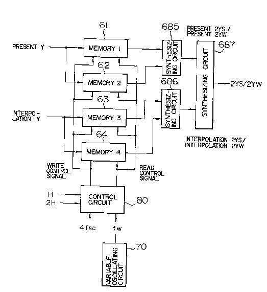
Fig. 7 is a block diagram of a video signal
10 processing apparatus in an embodiment of the invention.
Reference numerals 61 and 62 denote the l-line
memories for speed conversion of a present line signal;
63 and 64 the l-line memories for speed conversion of
an interpolation line signal; 685 a synthesizing circuit
15 of outputs of the memories 61 and 6Z; 686 a synthesizing
circuit of outputs of the memories 63 and 64; 687 a
synfh~; 7;nq circuit of outputs of the synthesizing
circuits 65 and 66; 70 a variable oscillating circuit to
variable generate the read clocks fw; and 80 the control
20 circuit to control the memories 61 to 64.
Even-number designated bits in the digital data
of the present line signal are written in~o the memory
61, for instance, while odd-number designated bits are
written into the memory 62. The same shall also apply
25 to the memories 63 and 64 for the interpolation line
signal. Control signals from the control circuit 80 are
derived from a circuit construction as shown in Fig. 8.
-- 10 --
~ 2046049
Reference numeral 81 denotes a frequency divider to
divide a horizontal sync signal H into 1/2; 82 to 85
shift registers to shift an output of the frequency
divider 81 at a period which is twice as large as that
5 of the horizontal sync signal H; 86 a circuit to produce
the write reset signal WRST; 87 a circuit to produce the
read reset signal RRST of the present line data; and 88
the circuit to produce the read reset signal RRST of
the interpolation line data. Those signal producing
10 circuits produce the respective signals in accordance
with the use of the memory. Reference numeral 89 denotes
an RE signal qenerating circuit to produce the read
enable (RE) signal to control the reading operations of
the memories 61 to 64.
The operation of the video signal processing
apparatus constructed as mentioned above will now be
described hereinbelow on the basis of timing charts
shown in Figs. 8 and 10. Fig. 9 shows waveforms in the
case where, for instance, a video image of the aspect
20 ratio of 4: 3 is double-speed converted and is fully
displayed onto the CRT screen of the aspect ratio of
9: 16.
The present line signal (present Y) and the
interpolation line signal (interpolation Y) which have
25 been processed and generated by the signal processing
circuit 5 are written into the memories 61 to 64, which
are reset by the write reset signal WRST every 2H, by
the clocks of 14.3 MHz (= 4fsc) (actually, 7.15 MHz in
21~4~
consideration of the relation of the operating frequency
of the memory).
The reading operations of the memories 61 to
64 are executed by using the present read reset signal
5 present RRST which is generated every 2H with a delay
time of lH from the write reset signal WRST and by using
the interpolation read reset signal interpolation RRST
which is further delayed by 0 . 5H from the present RRST .
At this time, since the present line data and the inter-
10 polation line data are controlled by the read enablesignals RE (present 2RES and interpolation 2RES), they
are read out by the clock frequency fw = 28 . 6 MHz
(8fSC) or 14.3 MHz every 910 dots and every 0.5H and
are synthesized by the synthesizing circuits 685 and
15 686. Thus, the present line signal (present 2Ys) and
the interpolation line signal (interpolation 2Ys) which
have been double-speed converted can be obtained as
outputs. Further, by synthesizing them by the synthesiz-
ing circuit 687, the final video signal 2Ys can be
20 obtained.
sy changing the frequency of the read clocks
fw~ the video signal can be compressed and displayed.
Fig. 10 shows waveforms in the case where the read clock
frequency fw is set to (fw = 8fSC x 16/12) and the
25 video image of the aspect ratio of 4: 3 is compressed
and displayed onto the screen of the aspect ratio of
9: 16 as shown in, for example, Fig. 2.
The read clock frequency fw is different from
-- 12 --
z0460a~9
that in Fig. 9 and the widths and the generating
positions of the read enable signals (present 2REW,
interpolation 2REW) differ from those in Fig. 9. The
write reset signal WRST and the read reset signals
5 (present RRST, interpolation RRST) are similar to those
in Fig. 9.
The processes such that after the video data
was written, it is read out lEI later denote that the
data has already been written by an amount of lE~. There-
10 fore, even if the data is compressed and read out, noproblem will occur.
On the other hand, the read enable signal for
the present line signal and the read enable signal for
the interpolation line signal are alternately generated.
15 The read enable signals RE are obtained by counting 910
clocks. As the clock frequency rises, the widths of
the read enable signals RE are narrowed. Therefore, by
making the count start position variable, the picture
plane is always located at the center of the CRT
20 irrespective of the clock frequency.
By synthesizing the data from the memories 61
to 64 by the synthesizing circuits 685, 686, and 687,
the double-speed converted video signal 2Ys or the video
signal 2YW which had been double-speed converted and,
25 further, has been compre~sed thereafter Ls obtained.
By the above construction, the number of
memories can be reduced and not only the simple double-
speed but also the further compression can be executed.
-- 13 --
2046049
Since the compression is performed by also including
the sync signal, it i5 impossible to set to 31.5 kHz in
such a state. Therefore, only the video signal component
in the compressed data is left and the sync signal and
5 the portion which lacked due to the compression are
replaced to the other data.
In the embodiment, four l-line memories have
been used. ~owever, if one 2-line memory is used for
the present line signal and one 2-line memory is used
10 for the interpolation signal, the number of memories can
be further reduced. there is no need to use the syn-
thesizing circuits 65 and 66 and the circuit construction
can be further simplified.
As described above, according to the invention,
15 the double-speed scan conversion and, further, the
compression converslon at an arbitrary reading speed can
be realized by the same circuit. The number of memories
can be reduced and the peripheral circuit construction
can be simplified.
-- 14 --