Note : Les descriptions sont présentées dans la langue officielle dans laquelle elles ont été soumises.
r~ ~
55~967
P~OGR~qA~I E IN~SE T3:~E DÆI~Y CIRCU:l T
Thi~ invenltion relate~ to a protection circuit
Pox ~lectrical and ~l~ctrot ~c: sy~temR and, mor~ par-
ticularly, to an invsr~e ti~e de~lay circuit ~or d~tec:ting
5 an overcurrent or oYarvoitage fault conditioll to protec:t a
powe:r 3witchlng d~vice.
E51ectrlc power ~y~t~as, 8Uch as single~ or
D~ult~ple l~ha~a AC or DC voltag~ ~y~te~, are required to
l~e op~srat~d ovar a rangs of conditic)Tls li~ilted by ~he
10 curr~n~ handl ing capz1 city o th~ wiring and loads .
Protective~ devic~ such a~ oolid stat~ power con~rollers
ar~ requir~d to sen~e ovorcurr~nt or overvoltagQ c~ndi-
t ion~3 in ~ sy~t~m~ and ~co operate to provlde any
reguired i~olation or rQconn~c:tio~ o~ the various sy~em
1 5 compo~ ts .
Su~lh prot~c:tiv6~ d~vic~ ~nay includ~ a trip
c:~r~ult ~his:h controls th~ operation o~ a ~:witchin~ device
in r~0pon~3 to a ~n~ed ov~rYolta~Q or oYercurrent
condltion and inolud~ an i~ver~e ~i~e del~y c:ircuit that
20 provl~ txlp ~ v~r~3u~ inpuk qiven by th~ Eqtuatl2n:
T ~ a~ ~1~
w~ere T 1~ th~ ltrip ~i~1119 O~ ~h~3 circuil: 7 X i~ g-
nitude~ o~ an input oignal r~pr~s~n~ativ~ Or vol~g~ or
current; and A, E~ and C ar~ eon~an~ n lnvers@ trip
25 c:irc:ui~ which pro~Tids~3 a ~rip ~i~e! in accordance wi~h the
:ESquation (1) is illuas~tra~s~d in U.~ Patellt NQ. 3,697,813,
i~ued October 10, 1972. ~ha con~t~nt B, ~hich may be a
Pirst referQnce voltage 1~3vel in th~ c$rcui~, dePines the
"'~
2 0 ~ r~
2 55,967
in~tantan@ou~ trip tim~a oi~ the circuit and the constant C,
which ~ay b~ a sec:ond xeference voltag@ lev~l, de~ines th~
ultimate trip time, wh~re the t:rip ti~lll8 apprOaGheS
inf inlty . Th~ con~tant A is a scal ing ~actor which
5 adjust~; th~3 spacing b~twaen the instant trip time and the
ultimat~3 trip ~imQ"
An additional trip c~rauit which provides a trip
ti~ne in 2~ccordance ~ h Equation (1) i~ illustrated in
block 3~ 0~ Figure ~ of U.S. Patent No. 4,245/1~4, issued
January 13, 198~Lo T~at c:ircuit include~ a noninverting
integrator which rec~iv~s a signal r~presentatlve o~ an
ov~rload condition and al~o r~aceiv~a~ a reference signal 1:o
produc~ a control 3ignal ~alt is proportional to th~
integral o~ the dif~erenca between tha overcurren~ siç~aal
and the rEafer~sncQ ~3ignal. Thi~ c:olltrol signal is co~pared
~o an ad.ditional raPerenca signa:L to produ~ trip signal
which chang~s lo~ic st~t~ when the~ magnitude o~ the
control E3ignal 2xc~ds the magnitud~ o~ the ~econd
r~rence slgn~l.
Such circuil:~ prov~dQ the d~ir~d in~rerse time
d~lay trip -qignal but ar~ d~a~ign~d to addres~ a ~ingle s~t
o~ operat~ ng p~ra~eters . Ther~ora r a large ~lumbsr oP
~uch t:ir~uit~ ~uæt b~a pro~id~d to addrss~ variou~ operat-
ing spec~ atlon3. It would be d~sira~l~ to devisa an
inv~r~ d01lay t1rip cir~uit which i~ capable of
~ati~acl:ory op~ratioll over a range o~ operating condi-
tlons to rQd~ e th3~ r~quir~d ~n~entory of such circuits.
S~Y QF T~ TI0
I~v~r~e ~ lel~y circui~ con tructed ln
3 0 accordanc~ ~1th thi~ invention inc:1ud~ an integrator
having a ~ir~t input ~or rec31ving a signa1 repre entative
o~ ~ vol~agQ or ~urr~nk in an ex~erna1 circuit aald having
~ 8~scond ~nput for raceiving a re~er~nce s~iqnal, 6uch tha~
the int~grator produce~ a con1:rol 8ign~1 rlapreal~ntativ~ of
the integra1 of th~ di~arenc~ o~ tA~ si~al~ at the
~irst ~nd s~cond inl?u~s~ A co~para~or is connected to
rec~laive the c:onkrol s1gna1 and to compare it with a second
referenc3 signal to produc~ an output signal which changes
2~0 ~7
3 55,967
stat~E; when the magnitudLs o~ control signal
eac^-~eds th~ rlagnitude c~f ~e ~econd re~rence signal. A
programmabl~ devic~ i~ provid~d to control th~ magnitudes
o~ either the flr~t rs~erenc~ ~ignal, th~3 second re~rence
signal, or both re~arons:~ ~ignal~ ~o that ltha instan~
taneou~ trip ti~e, th6~ ulti~ealte trip time, or both trip
times can b~a controlled eithe~r togeth~r or independen~ly
to provide an inver~e ti~e delay circuit that i~ capable
o~ operating over a wid~ rang~ o~ ~pe,cifiedl operating
aondition~.
~I~F DESCRIPTIO~I O~ TEIE: DR~wINç:s
Th~ inv~ntion wi.ll bes:ome ~nore readily apparent
~rom the ~ollowing d~cript~ on o~ th~ ~regerred embodi-
ments th~reof, ~hown ~n th~ acco~panying dra~ings wh~rein:
Pigures 1, 2 and 3 are sch~matic diagra:~ of
alternativ~ embodiD~ents o~ the prasan~ invntion; and
F~r~ 4 i~ a ~er~ ~9 of curves which illustrate
thQ opera~ion o~ the circuit3 o~ ~igur~ and 3.
~ ~ ~RREr) ~DI~3N~S
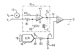
Re~erring to th~ drawings, Figure 1 i3 a
schematic: diagram o~ ona embodimQnt o~ an inverse time
d~lay circuit constructed in zlccorslance with the pre~ent
invent~on. ~rh~ c:ircuit i~cluda~ an integrator 10 compris
ing op~ration~l a~plii~i~r Ul, c~paci~or C, and re~istors
~5 Rl ~nd lR27 A l3ignal V~ rapr~ntativ~ o~ a vol~age or
curr~nt ~ al in an e~ternal ~ircu~t i~ D~ultipliad by a
~calins~ ~as::tor ~ by a scaling circuit 12 and connect~d to
~o~ir:lv~ ng input o~E op~rational asnpli~i~r ~1. A
~irst r~r~nael ~ignal Vl i8 ~upplied ~s~ ~e in~er~ing
input o~ ~apli~i~r Ul. Thi3 r~sults in a control ~ignal
on lin~ 14 whlch i~ repr~n~ativ~ o~ th~ in~ral o~ the
dif~er~nce be~w~en 1~ l~al~ at ~e irlverting and
noni~vertinSI inpu~3 o~ ~hQ opç~rationa~l amplifier U1. A
~omparator U2 r~c6~1v~s t}l~ control signal on 1iR13 14 and
compare~ it to a ~cond r~ rence signal V2 to produ~:s an
output signal ~O which ~oQ~; ~ro~ a logi :: low tc~ a logic
high level wh~n t~e m7~qn$tude o~ cc\rltrol signal
exce~ds th~ magnitudQ o~ second r~erenc~ signal. The
2 ~
4 55, 967
circuit of P~re 1 provides a challgs in logic sta~ o~
the output ~i~nal SO at a trip ti~ ~ in accordance ~ith .
~3~uation (1~ above. Th~ ccnstant~ A, B an~ C of Equatior
(1) can now be deter~ained in accordanca wi~ the parame-
5 tar~ o~ ~3 circuit o~E F~ ~ar~ î a~ ~ollow~ . Ai: thein~tant txip leYel ~ where X 5~ B ~
Vo (~ V~ + B~ v2 ( 2 )
~r2~1
~V~ Rl t R2
1 ( V2Rl ! (5)
At the ulti~ulte t~lp 1l3va31, wh~3n X ~ C:
XC 5' ~1 (6)
~: ,, ;L ( 7 )
~q~uation~ (5) and (7) can be us~d to d~3sig~ or
an~lyz~ci.~cuit o~ 1. An analysis of these
~guation~s ~how~ that l:h~ in~t~Tatan~ou trip l~v~l ~s
co~roll~d ~ m~gnituda o~ thQ ace~nd rQ~rence signal
V2. ~ an~log to digital con~art~r 16 is u~ to provid~
thet abillty ~o progr~ agnituds o~ sis~nal V2 ~y
20 rec~iving a digitzll com~and sign~l OTI line~ 18 to produce
a progr~m6~d r~r~c~ voltag~ ~ on 1 ~ne ~ O . This
programm~d ~ef~rence voltaga i~ d~liver~d ~o a res$s~ive
Yoltage dlvid~r com~ri~ing r~ 0:Y8 ~3 and :R~ such ~cha~
r~ference ~ignal V2 i~ produced at th~ ~unction point
25 b~tween r~si~tor R3 al~d R4. Th~ R3, R4 voltage divider
Dla~ch~ ypical 0-10 volt rang~ o~ digi~al~to~;
analog con~rt~r to th~ re;auir2d range ~ ~J2 v~lue~.
2 ~
55, 967
Figur~ 2 is a schemal:ic diagram of arl alterna
tiv~ o~iment o~ the invention wherein both the in~tan-
tan~ou~ trip an ultimate trip levels ~re programmable.
Thi~ i~ acco~plished by ad.ding a 3econd r~istiv~3 voltage
5 divider compri~ing th~ ~erieæ conn~ction of resi~toE~ R~
and R6 ~uch tha1: the ~rst re~ç~rence voltag~ Rignal V
appears at the ~unation point between resi~tors ~R5 and R6.
~gua ion~ (5) and (7~ ~ho~ th~t con~tanta B and C will
c:hang~ tos~ether i~ Vl and V2 ax2 both mada proporkional ~o
10 Vp.
FigurQ 3 i~ a sche~m~tic diagra~ o~ ~nother
eD~c~dimant of th~ present i~rention in which the ultin~ate
trip level C i~ programmable. Thi~ i~ a~complished by
addlng r~is~or R7 l~etwaen the output o~ integrator 10 and
15 l:h~ noninver~inS~ lnput o~ co~parator U~, aald by adding a
ra~istor R8 I:~t~en the output o~ th~ digital-to~analog
convert~r 16 and the nonin~rerting input Or comparator U2~
A r~renc~ voltaga V3 i~ suppli~d tQ th~a inv~srting input
oP co~parator U2. From Equ2ltion (5), it can b~ seen that
20 ch~ngin~ t,he~ valua o:t~ the r~ferenc~a signal Vl al~o changes
value o~ ~on tant ~changing ~ i~ not de lrable,
~e s~cond r~I~rence signal V2 DlU t lbQ modif iad ~ Vp to
~ake th~ ln~tantan~ us trip leYel B indep2ndent of the
~ ang~ in V~, and thu~ ind~perldent o~ chang in
25 consta~t C. Irl ~ c~rcu~t of Flguro 3, t~ values of
r~ tor~ ~7 and R8 are ch~3n ~o DlaX~ in~tantaneous
~ v~l irdep~ndent o~ the n~agnitu~ of l:h~ progra~med
volt~g~ ~,. ma retauir~d ratio o~ r~i6tor~ R7 and R8 is
~oun~ by:
3~ ~BZ, p (1 ~ ~) (83
wh~re th~3 p i~ ths rat1o o~ Vl to Vp. q~h~n, V3 i8 ~ound
by th~ Equationo
V R8 + V R7
V3(R7 ~ R8 ) ( 9 )
2 0 ~: 6 ~ r~J 7
6 55, 967
whe~r~ V2 18 th~ ra~rence value a~umed in ~he de~ign of
th~ ci3:6uiLl: oi~ Figur~ 1.
Flgur~ 4 i~ a ~ri~s o~ cunre~ which illu~trate
th~ programmable capabilitie~ o~ the circuits o~ Figures
5 1, ~ and 3. Curve 22 ~how~ an operating characteristic
for thQ circuit of Figure 1 i~ i8 a pre~elected f ~ xed
~alue . Curve 2 4 ~hows the re~ult of increas.ing t~e entire
trip c:haracteristic by a fac:tor o~ 2. ~30th th~3 ultimate
tr:Lp and instanlt trip lQ~els have been increased by the
10 same amount, Curv~ 26 shows the re~ult of d¢crea ing the
in~tantaneo;l~ trip level by a ~actor o~ 2. The ultimate
trip lev~l remain~ unchang~d. Curve 28 ~how~ the r~;ults
of increa~ing th~ ultimate trip le~l by a fac:tor of 2
whil~ maint~ining 'ch~ orlginal in~tant ~rip l~v~l.
The~ results illu~trated by the cunres o~ Fiçlure
4 ~how 1:hat complete ~lsxibility in programming the trip
charactQri~tic i~ availabla if th~s dla~cribad t~c}mique~
are u~d. Inverse ti~e delay trip circuits con~tructed in
accordanc~ with thi~ invention pro~ridQ program~able trip
2 0 characteri~tics by u~ing prograDullabl~ r~îerence voltage
l~vel3. Tha ultimate trip and ~ natant ~rip lhvel~ may be
pros~ra~m~d indep~ndently, and ~-a required circuit
~o~pon~I~t ~alu~ can be~ ~a~ily calculatad.
Althoug~ the p~es~nt in~ention ha~ been sho~n in
25 t~rme o~ ~hat ~r~ at present b6~ v~d to b~ its pr ferred
e~bodi~nt~, it will b~a appar~nt to ~ho~e ~klll~d in the
~rt ~ariou~3 eh~ng2~ luay be made withou~ d~partiny from lthe
0p~ o~ n1:ionO For ~xa~ple, althous~h a digi1:al-
to~ analog ~:onv~rt~r i9 ~ho~m to provid~ e programmabla
3 0 v olt~ag~ r~r~nc~ l~v~l Vp, an analog C:iXCllit which
adjust~ th~ voltag~ m~y b~ u~d in E~lac~ of the
dis~ital-to~analog c:onvart2r. It iE~ therl3fore i~tended
~hat th~ appended c:laims cvver such change~.
, ..
,