Note : Les descriptions sont présentées dans la langue officielle dans laquelle elles ont été soumises.
- FJ-8630
2048237
1 --
APPARATUS FOR SUPPLYING CURRENT TO LASER DIODE
WITH AUTOMATIC POWER CONTROL
R~C~ÇROUND OF THE lNv~NllON
l) Field of the Invention
The present invention relates to an apparatus
for supplying a current to a laser diode, to cause the
laser diode to emit a light to be used when reading
digital data from an optical storage medium and when
writing digital data thereto.
2) Description of the Related Art
Recently, many optical storage devices using
an optical storage medium such as an optical disk, an
optomagnetic disk, and an optical memory card have been
developed. In such optical storage devices, a laser
diode is used as a light source when carrying out a read
operation and a write (erase) operation. For example,
during a write mode, a laser beam is made incident on an
area of a magnetic film of an optical storage medium
which has been premagnetized, and as a result, that area
of the magnetic film is heated, and accordingly, the
direction of magnetization therein is inverted by the
affect of magnetization of adjacent areas thereof.
Also, during an erase mode, a laser beam is made
incident on an area of the magnetic film, to heat same,
and the heated area is then magnetized by using an
external bias magnetic field. During a write or erase
mode, a laser beam is used as the source of heat, and
therefore, the driving of a laser diode for generating
such heat requires a large amount of energy. On the
other hand, during a read mode, when a laser beam is
made incident on an area of the magnetic film, the read
data is determined by a change in a plane of
polarization of a reflected light, due to the Kerr
effect. During a read mode, a laser diode for
generating a laser beam is driven by a small amount of
~ ~ - 2 - 2048237
energy.
When the laser diode is driven by a small
amount of energy, the output level of the laser diode is
in a noise region, and the S/N ratio of a reproduced
signal is low. Therefore, to enhance this S/N ratio, a
current supplied to the laser diode is modulated by a
high frequency signal having a frequency much higher
than a frequency used for recording data in the magnetic
film, to enhance the peak of current supplied to the
laser diode without increasing an effective output of
light therefrom.
Also, to suppress fluctuations in the output
of light emitted from the laser diode, an automatic
power control (APC) is adopted, to bring a mean value of
a light output during a read mode and a minimum light
output (called a base read output) during a write mode
close to a desired level.
In the above-mentioned laser diode drive
system using an APC, although the desired level of the
APC is not changed even when the control is transferred
from a read mode to a write (or erase) mode, or vice
versa, the drive current of the APC is changed, since
the drive current of the laser diode, i.e., the
illumination thereof during a read mode, is AC, and the
current provided during a write mode for a base read
output is DC. Therefore, upon a switching between a
read mode and a write (or erase) mode, the control of
the light output is unstable due to a delay in the
response caused by a time-constant of the APC, to thus
reduce a speed of an access to the optical storage
medium, as later explained in detail.
SUMMARY OF THE INVENTION
An object of the present invention is to avoid
fluctuations in the APC upon a switching between a read
mode and a write (or erase) mode, to thereby enhance a
speed of access to an optical storage medium upon such a
switching.
- _ ~ 3 ~ 2048237
- According to the present invention, an amount of
current is supplied to a laser diode during a read mode
and during a write mode, and this predetermined current
is not larger than a threshold current (miniml1m current)
which causes the laser diode to emit light. During a
read mode, a read peak current modified by a high
frequency signal in addition to the amount of current is
supplied to the laser diode, and during a write mode, a
base read current in addition to the amount of current
is supplied to the laser diode, so that a light output
of the laser diode is equal to a base read output. The
read peak current is adjusted so that a mean value of
the light output of the laser diode is equal to the base
read output, and an automatic control is performed upon
the amount of current so that the light output of the
laser diode is close to the base read output. As a
result, when the control is transferred from a read mode
to a write tor erase) mode, or vice versa, since the
mean value (effective value) of the light output during
a read mode coincides with the light output (base read
power) during a write mode, the drive current of the
laser diode is not substantially changed. Therefore,
the monitored output of light is not substantially
changed, and thus the operation of the APC is stable.
Thus, even after the control is switched, a read or
write access is immediately initiated.
Note, in an erase mode, although the light output
is considerably larger than the base read output, a
current is absorbed by other means from a monitored
light output tcurrent) supplied to the APC.
Accordingly, the operation of the APC is stable at a
switching of the control from a read mode to an erase
mode or vice versa.
BRIEF DESCRIPTION OF THE DRAWINGS
The present invention will be more clearly
understood from the description as set forth below, with
reference to the accompanying drawings, wherein:
~ ~ 4 ~ 2048237
Fig. 1 is a block circuit diagram illustrating
a prior art apparatus f or supplying a current to a laser
diode;
Fig. 2 is a graph showing a supplied current
and a light output characteristic of the apparatus of
Fig. 1;
Figs. 3A and 3B are timing diagrams showing
the operation of the apparatus of Fig. 1;
Fig. 4 is a circuit diagram illustrating a
f irst embodiment of the apparatus f or supplying a
current to laser diode according to the present
invention;
Fig. 5 is a logic circuit diagram of the gate
circuit of Fig. 4;
Fig. 6 is a circuit diagram of the APC circuit
of Fig. l;
Fig. 7 is a circuit diagram of an example of
the control current sources (voltage/current conversion
circuits) of Fig. 4;
Fig. 8 is a circuit diagram of an example of
the current switches of Fig. 4;
Figs. 9 through 14 are f lowcharts showing the
operation of the microcomputer of Fig. 4;
Fig. 15 is a diagram showing a current
supplied and a light output characteristic of the
apparatus of Fig. 4;
Fig. 16 is a circuit diagram illustrating a
second embodiment of the apparatus for supplying a
current to laser diode according to the present
invention;
Fig. 17 is a logic circuit diagram of the gate
circuit of Fig. 16;
Fig. 18 and 19 are flowcharts showing the
operation of the microcomputer of Fig. 16, and
Fig. 20 is a diagram showing a current
supplied and a light output characteristic of the
apparatus of Fig. 16.
2048237
DESCRIPTION OF THE PREFERRED EMBODIMENTS
Before the description of embodiments of the
present invention, a prior art apparatus for supplying a
current to a laser diode will be explained with
reference to Figs. 1, 2, 3A, and 3B.
In Fig. 1, which illustrates a prior art apparatus
for supplying a current, reference numeral 1 designates
a laser diode connected to two parallel control current
sources (voltage to current conversion circuits) 2-1 and
2-2, which receive voltages V1 and Vw / respectively,
from a microcomputer or the like (not shown).
The control current sources 2-1 and 2-2 are
switched by current switches 3-1 and 3-2, respectively.
During a read mode, the current switch 3-1 is
switched by using a high frequency signal HFM supplied
from a high frequency signal generator 4. In this case,
the frequency of the high frequency signal HFM is much
higher than a frequency used for recording data to the
optical storage medium (not shown). As a result, a
modified current having a read peak current IHFM in
addition to a threshold current Ith is supplied to the
laser diode 1, to thereby obtain a read peak output
PHFM , as shown in Fig. 2.
During a write mode for data '~0" (WDT = "0"), a
base read current IR in addition to the threshold
current Ith is supplied to the laser diode 1, to thereby
obtain a base read output PR , as shown in Fig. 2.
During a write mode for data "1" (WDT = "1"), the
current switch 3-2 is turned ON by a write data signal
WDT, and as a result, a write current IW is added to a
current (Ith + IR) flowing in the laser diode 1, to
obtain a write output PW ~ as shown in Fig. 2.
Also, during an erase mode, the current switch 3-1
is operated under a write mode, and the current switch
3-2 is operated under a write mode for write data "1"
(WDT = ~1"), and therefore, a current Ith + IR + IW is
continuously supplied to the laser diode 1.
2048237
_ - 6 -
An APC circuit 4 carries out an automatic power
control of a current flowing through the control current
source 2-l so that a voltage VM showing a light output
of the laser diode l monitored by a photo diode 5 is
close to the voltage VR showing the base read output PR.
Thus, a fluctuation of the light output of the laser
diode l due to a change of temperature, an elapse of
time, and the like can be suppressed.
In the above-mentioned prior art apparatus for
supplying a current, however, when the control is
transferred from a read mode to a write mode, or vice
versa, the control of the output of the laser diode l by
the APC circuit 4 is actually fluctuated.
For example, as shown in Fig. 3A, when the control
is transferred from a read mode to a write mode for
data "0", a current supplied to the laser diode l is
changed from a modulated current IMoD to a definite
current Ith + IR ~ even when the voltage VR is definite.
As a result, a light output of the laser diode l is
fluctuated, to thereby apply noise, as a monitored
output, to the APC circuit 4, and thus, the operation of
the APC circuit 4 becomes unstable. Such an unstable
operation state of the APC circuit 4 continues for a
time Tl , depending on a time constant of the APC
circuit 4, and for this time Tl , it is impossible to
obtain a write access to the optical storage medium, and
therefore, at worst, such a write access is initiated
after one more rotation of the optical storage medium.
Similarly, as shown in Fig. 3B, when the control is
transferred from a write mode for data "0" to a read
mode, a current supplied to the laser diode l is changed
from the definite current Ith + IR to the modulated
current IMoD even when the voltage Vl is definite. As a
result, a light output of the laser diode l is
fluctuated, to thereby apply noise, as a monitored
power, to the APC circuit 4, and thus, the operation of
the APC circuit 4 becomes unstable. Such an unstable
- 7 - 2048237
operation state of the APC circuit 4 continues for a
time T2 ~ depending on the time constant of the APC
circuit 4, and for this time T2 r it is impossible to
obtain a read access to the optical storage medium, and
therefore, at worst, such a read access is initiated
after one more rotation of the optical storage medium.
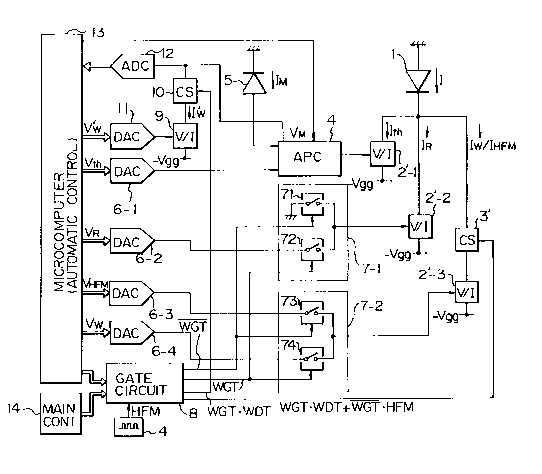
In Fig. 4, which is a first embodiment of the
present invention, three control current sources 2'-1,
2'-2, and 2'-3 are provided, and a current switch 3' is
connected in series to only the control current
source 2'-3.
The control current source 2'-1 is used for
supplying a threshold current (minimum current) Ith (see
Fig. 15) by which the laser diode 1 initiates the
emitting of light therefrom. The APC circuit 4 is
connected to only the control current source 2'-1, and
therefore, an automatic power control is carried out for
the threshold current Ith in accordance with a
difference between a voltage Vth supplied by a
digital/analog (D/A) converter 6-1 and a monitored
voltage VM supplied by the photo diode 5. The control
current source 2'-2 is used for supplying a base read
current IR (see Fig. 15) to the laser diode 1 during a
write mode (WGT = "1" ), while not supplying a current
during a read mode (WGT = "1" ) . For this purpose, a
switching circuit 7-1 formed by two switches 71 and 72
is provided. That is, during a write mode, when a gate
signal WGT (= "1" ) is supplied from a gate circuit 8 to
the switch 72, a voltage VR corresponding to the base
read current IR is applied by a D/A converter 6-2 to the
control current source 2'-2. Note that, when a
current Ith + IR is supplied to the laser diode 1, the
light output is the base read output PR (see Fig. 15).
On the other hand, during a read mode, when a gate
signal WGT ( = " 1 " ) is supplied from the gate circuit 8
to the switch 71, 0 V is applied to the control current
source 2'-2.
- _ - 8 - ~048~37
The control current source 2'-3 is used for
supplying a read peak current IHFM (see Fig. lS) during
a read mode (WGT = "l") and supplying a write current IW
during a write mode for data "l" (WGT = WDT = "1"). For
this purpose, a switching circuit 7-2 formed by two
switches 73 and 74 is provided. That is, during a read
mode, when the gate signal WGT (= "l") is supplied to
the switch 73, a voltage VHFM corresponding to the read
peak current IHFM is applied by a D/A converter 6-3 to
the control current source 2'-3. Also, in this case,
the current switch 3' is switched by the high frequency
signal HFM, and therefore, the read peak current IHFM is
modulated by the high frequency signal HFM. Note that,
when a current Ith + IHFM is supplied to the laser
diode l, the light output is the read peak output PHFM
(see Fig. 15). On the other hand, during a write mode
for data "l", when the gate signal WGT (= "l") is
supplied to the switch 74, a voltage Vw corresponding to
the write current IW is applied by a D/A converter 6-4
to the control current source 2'-3. Also, in this case,
the current switch 3' is turned ON by the signal WGT.WDT
(= "l"). Note that, when a current Ith + IR + IW is
supplied to the laser diode l, the light output is the
write output PW (see Fig. lS).
In the APC circuit 4, the threshold voltage Vth by
the D/A converter 6-l is applied to one input and the
monitored power voltage VM is applied to another input.
Therefore, the threshold current Ith flowing through the
control current source 2'-l is adjusted by the APC
circuit 4 so that the monitored light output voltage VM
is brought close to the threshold voltage vth. Note
that a current to voltage conversion circuit is actually
required to convert a current IM flowing through the
photo diode 5 to the monitored output voltage VM at a
prestage of the APC circuit 4, but such a conversion
circuit is omitted for a simplification of the circuit.
Also, such a conversion circuit can be included in the
2048237
APC circuit 4 (see Fig. 6).
Also, a series of a control current source 9 and a
current source 10 are connected in series to the photo
diode 5. During a write mode for data "1", when a gate
signal WGT.WDT is supplied to the current switch 10, a
voltage Vw' corresponding to the write current IW is
applied by a D/A converter 11 to the control current
source 9. Therefore, even when a write current IW is
added to the current flowing through the laser diode 1,
an increase in the monitored output voltage VM due to
the write current IW is absorbed by the control current
source 9. Therefore, during a write mode (WGT = "1"),
the monitored light output voltage VM is maintained at a
value corresponding to the base read output PR ,
regardless of the write data. In this case, a
voltage Vw' corresponding to the above-mentioned
increase represented by a current Iw' is applied by the
D/A converter 11 to the control voltage source 9, and
thus, an abnormal operation of the APC circuit 4 due to
the write current IW is avoided.
Reference numeral 12 designates an A/D converter
for fetching the monitored output voltage VM. Also, in
this case, note that a current to voltage conversion
circuit is actually required to convert the current IM
flowing through the photo diode 5 to the monitored
output voltage IM at a prestage of the A/D converter 12,
but such a conversion circuit is omitted for a
simplification of the circuit.
A microcomputer 13, which is formed by a central
processing unit (CPU), a read-only memory (ROM), a
random access memory (RAM), and the like, is provided
for controlling the various elements in Fig. 4. This
microcomputer 13 is used only for an automatic
adjustment of the voltages Vth , VR , VHFM ~ V
and Ww'.
A main controller 14 is provided for actually
performing a read, write, or erase operation at the
- ~ lo - ~o 48~37
-
optical storage medium, after an automatic adjustment by
the microcomputer 13.
Thus, the gate circuit 8 can be operated by both
the microcomputer 13 and the main controller 14, as
illustrated in Fig. 5.
In Fig. 5, the microcomputer 13 supplies a gate
signal WGT1 during a write mode and a write data signal
WDT1 to the gate circuit 8, and the main controller
supplies a gate signal WGT2 during a write mode and a
write data signal WDT2. Also, a high frequency signal
HFM is supplied to the gate circuit 8.
The gate circuit 8 includes two OR circuits 81
and 82, an inverter 83, two AND circuits 84 and 85, and
an OR circuit 8 6. The OR circuit 81 generates a gate
signal WGT (= "1"), when the microcomputer 13 generates
a gate signal WGT1 (= "1") or when the main controller
14 generates a gate signal WGT2 (= "1"). In other
words, when one of the microcomputer 13 and the main
controller 14 is in a write mode, the OR circuit 81
generates the gate signal WGT (= "1"). Similarly, the
OR circuit 82 generates a write data signal WDT (= "1")
when the microcomputer 13 generates a write data signal
WDT1 (= "1"), or when the main controller 14 generates a
write data signal WDT2 (= "1").
The inverter 83 inverts the output WDT of the OR
circuit 81, and accordingly, generates a gate signal
WGT. Also, the output WDT of the OR circuit 81 is
directly output.
Since the AND circuit 84 is connected to the
outputs of the OR circuits 81 and 82, the AND circuit 84
generates a gate signal WGT-WDT.
Also, since the AND circuit 85 is connected to the
inverter 83 and receives the high frequency signal HFM,
the AND circuit 85 generates a gate signal WGT. HFM.
Further, since the OR circuit 86 is connected to
the outputs of the AND circuits 84 and 85, the OR
circuit 86 generates a gate signal WGT.WDT + WGT-HFM.
~ 11 2048237
Thus, the gate signals WGT, WGT, WGT.WDT, and
WGT.WDT + WGT.HFM are generated by the gate circuit 8.
In Fig. 6, which is a detailed circuit diagram of
the APC circuit 4 of Fig. 4, the APC circuit 4 includes
a differential amplifier 41 for converting a current IM
flowing through the photo diode 5 into a voltage which
is already indicated by VM , a differential amplifier 42
for generating a difference signal between the light
output voltage VM from the differential amplifier 41 and
the threshold voltage Vth from the D/A converter 6-1,
and an integrator 43. In more detail, the differential
amplifier 41 is formed by an operational amplifier 411
and a variable resistor 412. That is, if the current IM
is increased, to increase a current flowing through the
resistor 412, a voltage between the terminals thereof is
also increased. Thus, the differential amplifier 41
generates a voltage VM depending on the current IM with
reference to ~Vgg1. Also, the differential amplifier 42
is formed by an operational amplifier 421 and resistors
421 to 424. Also, the integrator 43 is formed by an
operational amplifier 431, a resistor 432, a
capacitor 433, resistors 434 and 435, and switches 426
and 427 controlled by the microcomputer 13.
The switch 426 is connected in parallel to the
capacitor 433, and the switch 427 is connected to a
non-inverting input of the operational amplifier 431.
Therefore, to release an APC, i.e., to turn OFF the APC
circuit 4, the microcomputer 13 turns ON the switch 426
and turns OFF the switch 427 as illustrated in Fig. 6,
so that the integrator 43 serves as a voltage buffer,
thereby applying the threshold ~oltage Vth to the
control current source 2'-1. On the other hand, to
carry out an APC, the microcomputer 13 turns OFF the
switch 426 and turns ON the switch 427, so that the
integrator 43 forms an actual integrator.
In Fig. 7, which illustrates an example of the
control current source such as 2'-1 of Fig. 4, the
_ - 12 - 2048237
control current source 2'-1 includes an operational
amplifier 701, resistors 702 through 706, and an output
transistor 707. Therefore, when a voltage such as the
threshold voltage Vth is increased, a current flowing
through the resistor 705 is increased, to thus increase
the base-emitter voltage VBE of the output
transistor 707. As a result, the current Ith flowing
through the output transistor 707 is dependent on the
threshold voltage Vth. In other words, the voltage Vth
is converted to the threshold current Ith.
In Fig. 8, which illustrates an example of the
current switches such as 3' of Fig. 4, the current
switch 3' includes two NPN transistors 801 and 802
having a common emitter connected to a current source
which is, in this case, the control current source 2'-3.
Also, a resistor 803 is connected between a collector of
the transistor 801 and a power supply such as the
ground. Further, a reference voltage VREF is applied to
a base of the transistor 801, and a gate signal such as
WGT.WDT + WGT.HFM is applied to a base of the
transistor 802. Therefore, if the potential of the gate
signal is lower than that of the reference voltage
VREF , the transistor 801 is turned ON and the
transistor 802 is turned OFF, so that a current I does
not flow. Conversely, if the potential of the gate
signal is higher than the reference voltage VREF , the
transistor 801 is turned OFF and the transistor 802 is
turned ON, so that a current I determined by the control
current source 2'-3 flows through the transistor 802.
After a power is supplied to the microcomputer 13,
the microcomputer 13 carries out an automatic control,
as explained below.
In Fig. 9, which is an automatic control routine
carried out after the power supply to the micro-
computer 13 is turned ON, at step 901, an initialization
is carried out. Particularly, the contents of Vth ,
VHFM , VR , VM , and Vw' in the RAM are cleared, and the
- - 13 - 2 0 4 8 2 3 7
data WGTl and WDT1 in the RAM are reset.
At step 902, the value Vth (i.e., Ith) for the D/A
converter 6-1 is determined, and at step 903, the value
VHFM (i-e-, IHFM) for the D/A converter 6-3 is
determined. Also, step 904, the value VR (i.e., IR) for
the D/A converter 6-2 is determined, and at step 905,
the value Vw (i.e., Iw) for the D/A converter 6-4 is
determined. Further, at step 906, the value Vw (i.e.,
Iw') for the D/A converter 11 is determined. Steps 902
through 907 will be explained later in more detail.
Next, at step 907, the data WGT1 and WDTl, which
are set at steps 904 and 905, are reset (= ~0").
Then, the routine of Fig. 9 is completed at
step 908.
In Fig. 10, which is a detailed flowchart of Vth
(Ith) determining step 902, the microcomputer 13 turns
OFF the APC circuit 4 at step 1001, so that the
threshold voltage Vth , which is, in this case, 0 V, is
supplied from the D/A converter 6-1 directly to the
control current source 2'-1. At step 1002, a monitored
power voltage VM is fetched from the A/D converter 12,
and at step 1003, the monitored output voltage VM is
converted to a power P of the laser diode 1 in
accordance with a predetermined function f.
At step 1004, it is determined whether or not P is
larger than 0, i.e., whether or not the laser diode 1
has initiated an emitting of light therefrom. As a
result, if P < 0, the control proceeds to step 1005,
which increases the value Vth by a definite value such
as 1, and the control at steps 1002 through 1004 is then
repeated. Otherwise, the control proceeds to step 1006,
thus completing the routine of Fig. 10. Thus, the value
Vth , i.e., the threshold current Ith is finally
determined by the routine of Fig. 10, and is stored in
the RAM.
In Fig. 11, which is a detailed flowchart of the
VHFM (IHFM) determining step 903, since the data WGTl is
~ - 14 - 2048~37
already reset (WGTl = "0") and the data WGT2 of the main
controller 14 is also reset (WGT2 = "0"), the value
VHFM , which is, in this case, 0 V, is supplied from the
D/A converter 6-3 via the switch 73 to the control
current source 2'-3. Also, in this case, the gate
signal WGT.WDT + WGT.HFM of the gate circuit 8
represents HFM, and therefore, the current switch 3' is
switched by the high frequency signal HFM.
First at step 1101, a mean value P of the monitored
power P is cleared.
Then, at step 1102, a monitored output voltage VM
is fetched from the A/D converter 12, and at step 1103,
the monitored output voltage VM is converted into a
power P of the laser diode 1 in accordance with the
predetermined function f.
At step 1104, the mean value P of the monitored
power P is calculated by
p n.P + P
n + 1
where n is a positive integer such as 3, 7, 15,
...... Of course, other calculation methods can be
adopted. Note that, in this case, the monitored power P
is an alternating current.
At step 1105, it is determined whether or not the
mean value P of the monitored power P is larger than a
base read output PR , i.e., whether or not the mean
value P equals the base read output PR. As a result, if
P _ PR ~ the control proceeds to step 1206, which
increases the value VHFM by a definite value such as 1,
and the control at steps 1102 through 1105 is then
repeated. Otherwise, the control proceeds to step 1107,
thus completing the routine of Fig. 11. Thus, the value
VHFM , i.e., the read peak current IHFM is finally
determined by the routine of Fig. 11 and is stored in
the RAM.
Note that, when carrying out the routine of
Fig. 11, a current I = Ith + IHFM is supplied to the
- 15 - ~ ~4~237
laser diode 1.
In Fig. 12, which is a detailed flowchart of VR
(IR) determining step 904, at step 1201, the gate signal
WGTl is set (WGT1 = "1"). As a result, the value VR ,
which is, in this case, 0 V, is supplied from the D/A
converter 6-2 via the switch 72 to the control current
source 2'-2. Also, in this case, the gate signal
WGT.WDT + WGT.HFM of the gate circuit 8 represents "0",
since WGT = "1", WDT = "0", and WGT = "0". Therefore,
the current switch 3' is turned OFF.
At step 1202, a monitored output voltage VM is
fetched from the A/D converter 12, and at step 1203, the
monitored output voltage VM is converted into a power P
of the laser diode 1 in accordance with the
predetermined function f.
At step 1204, it is determined whether or not P is
larger than PR , i.e., whether or not the light power P
equals the base read output PR. As a result, if P
~ PR ~ the control proceeds to step 1205 which increases
the value VR by a definite value such as 1, and the
control at steps 1202 through 1204 is then repeated.
Otherwise, the control proceeds to step 1206, thus
completing the routine of Fig. 12. Thus, the value VR
for the base read output PR is finally determined by the
routine of Fig. 12, and is stored in the RAM.
Note that, when carrying out the routine of
Fig. 12, a current I = Ith + IR is supplied to the laser
diode 1.
In Fig. 13, which is a detailed flowchart of the Vw
(Iw) determining step 905, at step 1301, the data signal
WDT1 is set (W1) T1 = ~1"). As a result, the gate
signal WGT-WDT + WGT.HFM of the gate circuit 8
represents "1", since WGT = "1", WDT = "1", and WGT
= '~0". Therefore, the current switch 3" is turned ON.
Also, in this case, since the gate signal WGT of the
gate circuit 8 is ~ , the value Vw r which is, in this
case, 0 V, is supplied from the D/A converter 6-4 via
- 16 - 2048237
the switch 74 to the control current source 2'-3.
At step 1302, a monitored output voltage VM is
fetched from the A/D converter 12, and at step 1403, the
monitored output voltage VM is converted into a power P
of the laser diode l in accordance with the
predetermined function f.
At step 1304, it is determined whether or not P is
larger than PW ~ i.e., whether or not the light power P
reaches the write power Pw~ As a result, if P ~ PW ~
the control proceeds to step 1205 which increases the
value VR by a definite value such as l, and the control
at steps 1402 through 1404 is then repeated. Otherwise,
the control proceeds to step 1406, thus completing the
routine of Fig. 13. Thus, the value Vw for the write
output PW is finally determined by the routine of
Fig. 13, and is stored in the RAM.
Note that, when carrying out the routine of
Fig. 13, a current I = Ith + IR + IW is supplied to the
laser diode 1.
In Fig. 14, which is a detailed flowchart of Vw'
(Iw') determining step 906, at step 1401, the
microcomputer 13 turns ON the APC circuit 4.
At step 1402, a monitored output voltage VM is
fetched from the A/D converter 12, and at step 1403, the
monitored output voltage VM is converted into a power P
of the laser diode 1 in accordance with the
predetermined function f.
At step 1404, it is determined whether or not P is
larger than PR , i.e., whether or not the light power P
is equal to the base read output PR. As a result, if P
~ PR ~ the control proceeds to step 1405 which increases
the value Vw' by a definite value such as 1, and the
control at steps 1402 through 1404 is then repeated.
Otherwise, the control proceeds to step 1406, thus
completing the routine of Fig. 14. Thus, the value Vw'
for an increased power due to the write current IW is
finally determined by the routine of Fig. 14, and is
- 17 - 2048237
stored in the RAM.
Note that, when carrying out the routine of
Fig. 14, a current I = Ith + IR + IW is supplied to the
laser diode 1.
The operation of the main controller 14 of Fig. 4
will be explained with reference to Fig. 15 which shows
a current I supplied to a light power P characteristic
of the current supplying apparatus of Fig. 4.
During a read mode, the main controller 14
generates a gate signal WGT2 (= "0"), and accordingly,
the gate circuit 8 generates a first gate signal WGT
(= "0"), a second gate signal WGT (= "0"), a third gate
signal WGT.WDT (= "0"), and a fourth gate signal WGT.HFM
+ WGT.WDT = HFM. By the first gate signal WGT and the
second gate signal WGT, the switches 71 and 73 are
turned ON, and the switches 72 and 74 are turned OFF.
Therefore, 0 V is applied to the control current source
2'-2, and the read peak voltage VR is applied to the
control current source 2'-3. By the third gate signal
WGT.WDT (= "0"), the current switch 10 is turned OFF,
and therefore, a monitored output current IM is not
absorbed in the control current source 9. By the fourth
gate signal HFM, the current switch 3' is switched by a
frequency of the high frequency signal HFM. As a
result, a current I = Ith and a current I = Ith + IHFM
is alternatingly supplied to the laser diode 1, and
accordingly, a read peak output PHFM alternatingly
appears as shown in Fig. 15. In this case, a mean value
P of a light power P of is brought close to the base
read output PR by an automatic power control of the APC
circuit 4, as shown in Fig. 15.
During a write mode for data "0", the main
controller 14 generates a gate signal WGT2 (= "1") and a
data signal WDT2 (= "0"), and the gate circuit 8
generates a first gate signal WGT (= "0"), a second gate
signal WGT (= "1"), a third gate signal WGT.WDT (= "0"),
and a fourth gate signal WGT.HFM + WGT.WDT (= "0"). By
2048237
- 18 -
the first gate signal WGT and the second gate signal
WGT, the switches 72 and 74 are turned ON, and the
switches 71 and 73 are turned OFF. Therefore, the
voltage VR is applied to the control current source
2~-2, and the voltage Vw is applied to the control
current source 2'-3. By the third gate signal WGT.WDT
(= "0"), the current switch 10 is turned OFF, and
therefore, a monitored output current IM is not absorbed
in the control current source 9. By the fourth gate
signal WGT.HFM + WGT.WDT (= "0"), the current switch 3'
is turned OFF. As a result, a current I = Ith + IR is
supplied to the laser diode 1, and accordingly, the base
read output PR appears as shown in Fig. lS. In this
case, a light power P1 is brought close to the base read
output PR by an automatic power control of the APC
circuit 4, as shown in Fig. 15.
During a write mode for data "1", the main
controller 14 generates a gate signal WGT2 (= "1") and a
data signal WDT2 (= "1"), and the gate circuit 8
generates a first gate signal WGT (= "0"), a second gate
signal WGT (= "1"), a third gate signal WGT.WDT (= "1"),
and a fourth gate signal WGT.HFM + WGT.WDT (= "1"). By
the first gate signal WGT and the second gate signal
WGT, the switches 72 and 74 are turned ON, and the
switches 71 and 73 are turned OFF. Therefore, the
voltage VR is applied to the control current source
2~-2, and the voltage Vw is applied to the control
current source 2'-3. By the third gate signal WGT.WDT
(= "1"), the current switch 10 is turned ON, and
therefore, a monitored output current IM is absorbed in
the control current source 9. By the fourth gate signal
WGT.HFM + WGT.WDT (= "1"), the current switch 3' is
turned ON. As a result, a current I = Ith + IR + IW is
supplied to the laser diode 1, and accordingly, the
write output PW appears as shown in Fig. 15. In this
case, a light power P2 / which is equal to the write
output PW minus ~P corresponding to the write
- 2048237
-- 19 --
current IW ~ is brought close to the base read output PR
by an automatic power control of the APC circuit 4, as
shown in Fig. 15.
During an erase mode, the main controller 14 always
generates a gate signal WGT2 (= "1") and a data signal
WDT2 (= "1"), in the same way as during a write mode for
data "1". Therefore, a current I = Ith + IR + IW is
supplied to the laser diode 1, and accordingly, the
write output PW also appears. Also, in this case, a
light power P2 ~ which is equal to the write output PW
minus ~P corresponding to the write current IW ~ is
brought close to the based read output PR by an
automatic power control of the APC circuit 4.
As shown in Fig. 15, the following condition is
satisfied:
IR ~ IHFM ~ IR + IW
Also, as shown in Fig. 15, the mean value P of the
light power P during a read mode is coincided with the
light power P1 and P2 during a write mode. Note that
both the light power P and P1 (P2) are brought close to
the base read output PR. Therefore, at a switching
between a read mode and a write mode (also erase mode),
an automatic power control by the APC circuit 4 is
hardly fluctuated.
In Fig. 16, which is a second embodiment of the
present invention, three control current sources 2'-4,
2'-5, and 2'-6 are provided instead of the control
current sources 2'-2 and 2'-3 of Fig. 4, and current
switches 3'-1, 3'-2, and 3'-3 are connected in series to
the control current sources 2'-4, 2'-5, and 2'-6,
respectively. Also, the switching circuit 7-1 and 7-2
and the D/A converter 6-2 of Fig. 4 are not provided,
and a D/A converter 6-5 is added.
The control current source 2'-4 is used for
supplying the read peak current IHFM to the laser
diode 1 during a read mode. Therefore, the read peak
voltage VHFM is applied by the D/A converter 6-3 to the
204~237
- 20 -
control current source 2'-4 and the current switch 3'-1
is turned ON in accordance with the high frequency
signal HFM during a read mode (WGT = "1"). However, the
current switch 3'-1 is turned ON even during a write
mode (WGT = "1").
The control current source 2'-5 is used for
supplying the write current IW during a write mode for
data ~ . Therefore, the write voltage Vw for the write
current IW is applied by the D/A converter 6-4 to the
control current source 2'-5, and the current switch 3'-2
is turned ON during a write mode for data "1" (WGT = WDT
The control current source 2'-6 is used for supply
a correction current IS to the control current sources
2'-1, 2'-4, and 2'-5, i.e., for subtracting the
correction current IS from a current I flowing through
the laser diode 1 during a write mode. Therefore, a
correction voltage Vs is applied by the D/A converter
6-5 to the control current source 3'-3, and the current
switch 2'-6 is turned ON during a write mode (WGT
= ~1~) .
A gate circuit 8' is obtained by modifying the gate
circuit 8 of Fig. 4.
In Fig. 17, which is a detailed circuit diagram of
the gate circuit 8' of Fig. 16, an OR circuit 86 is
different from the OR circuit 86 of Fig. 5. That is,
the OR circuit 86' is connected to the outputs of the OR
circuit 81 and the AND circuit 85. Therefore, the OR
circuit 86' generates a gate signal WGT + WGT.HFM.
Also, the gate circuit 8' does not generate the gate
signal WGT.
An automatic control by the-microcomputer 13 in
Fig. 16 is illustrated in Fig. 18. That is, steps 1801
and 1802 are provided instead of steps 901 and 902 of
Fig. 9. At step 1801, the value Vs instead of the value
VR is cleared. Also, at step 1802, the value Vs for the
correction current IS for the D/A converter 6-5 is
` _ - 21 - 2048237
determined.
In Fig. 19, which is a detailed flowchart of the Vs
(Is) determining step 1802, at step 1901, the gate
signal WGTl is set (WGTl = "1"), i.e., the gate signal
WGT is set (WGT = "1"). As a result, the current switch
3'-2 is turned ON, and accordingly, the read peak
current IHFM is supplied to the laser diode 1. Also,
the current switch 3'-3 is turned ON, and accordingly, a
correction current IS corresponding to the correction
voltage Vs which is, in this case, 0 V, flows through
the control current source 2'-6. Also, in this case,
the gate signal WGT.WDT of the gate circuit 8'
represents "0", since WDT = "1". Thus, the current
switch 3'-2 is turned OFF. Therefore, a current I = Ith
+ IHFM ~ IS is supplied to the laser diode 1. Here
S =
At step 1902, a monitored output voltage VM is
fetched from the A/D converter 12, and at step 1903, the
monitored output voltage VM is converted into a power P
of the laser diode 1 in accordance with the
predetermined function f.
At step 1904, it is determined whether or not P is
smaller than PR , i.e., whether or not the light power P
reaches the base read output PR. As a result, if P
> PR , the control proceeds to step 1905 which increases
the value Vs by a definite value such as 1, and the
control at steps 1902 through 1904 is then repeated.
Otherwise, the control proceeds to step 1906, thus
completing the routine of Fig. 19. Thus, the value Vs
for the correction current IS is finally determined by
the routine of Fig. l9, and is stored in the RAM.
Also, note that, when carrying out the Vw (IW)
det~rmining step 905 and the Vw' (Iw') determining step
906, a current I = Ith + IHFM ~ IS + IW is supplied to
the laser diode 1.
The operation of the main controller 14 of Fig. 16
will be explained with reference to Fig. 20, which shows
_ - 22 - 2048237
a current I supplied to a light power P characteristic
of the current supplying apparatus of Fig. 16.
During a read mode, the main controller 14
generates a gate signal WGT2 (= "0"), and accordingly,
the gate circuit 8' generates a first gate signal WGT
(= "0"), a second gate signal WGT.WDT (= "0"), and a
third gate signal WGT + WGT-HFM = HFM. By the first
gate signal WGT (= "0"), the current switch 3'-3 is
turned OFF, and accordingly, the correction current IS
does not flow. By the second gate signal WGT.WDT
(= "0"), the current switch 3'-2 and 10 are turned OFF,
and accordingly, the write current IW and the current
Iw' do not flow.
By the third gate signal HFM, the current switch
3'-1 is switched by a frequency of the high frequency
signal HFM. As a result, a current I = Ith and a
current I = Ith + IHFM is alternatingly supplied to the
laser diode 1, and accordingly, a read peak output PHFM
alternatingly appears as shown in Fig. 20. In this
case, a mean value P of a light power P of is brought
close to the base read output PR by an automatic power
control of the APC circuit 4, as shown in Fig. 20.
During a write mode for data "0", the main
controller 14 generates a gate signal WGT2 (= "1") and a
data signal WDT2 (= "0"), and the gate circuit 8'
generates a first gate signal WGT (= "1"), a second gate
signal WGT.WDT (= "0"), and a third gate signal WGT +
WGT.HFM (= "1"). By the first gate signal WGT (= "1"),
the current switch 3'-3 is turned ON, and accordingly,
the correction current IS flows through the control
current source 2'-6. By the second gate signal WGT.WDT
(= "0"), the current switches 3'-2 and 10 are turned
OFF, and accordingly, the write current IW and the
current Iw' do not flow. As a result, a current I = Ith
+ IHFM ~ IS is supplied to the laser diode 1, and
accordingly, the base read output PR appears as shown in
Fig. 20. In this case, a light power P1 is brought
-
- 23 - 2048237
close to the base read output PR by an automatic power
control of the APC circuit 4, as shown in Fig. 20.
During a write mode for data "l", the main
controller 14 generates a gate signal WGT2 (= "l") and a
data signal WDT2 (= "l"), and the gate circuit 8'
generates a first gate signal WGT (= "1"), a second gate
signal WGT.WDT (= "1"), and a third gate signal WGT +
WGT.HFM (= "1"). By the first gate signal WGT (= "l"),
the current switch 3'-3 is turned ON, and accordingly,
the correction current IS flows through the control
current source 2'-6. By the second gate signal WGT.WDT
(= "1"), the current switches 3'-2 and 10 are turned ON,
and accordingly, the write current IW is supplied to the
laser diode 1 and the current Iw' in the monitored
output current IM is absorbed by the control current
source 9. By the third gate signal WGT + WGT.HFM
(= "1"), the current switch 3'-1 is turned ON, and
accordingly, the write current IW is supplied to the
laser diode 1. As a result, a current I = Ith + IHFM ~
IS + IW is supplied to the laser diode 1, and
accordingly, the write output PW appears as shown in
Fig. 20. In this case, a light power P2 ~ which is
equal to the light power PW minus ~P corresponding to
the write current IW ~ is brought close to the based
read output PR by an automatic power control of the APC
circuit 4, as shown in Fig. 20.
During an erase mode, the main controller 14 always
generates a gate signal WGT2 (= ~'1") and a data signal
WDT2 (= "1"), in the same way as during a write mode for
data "1". Therefore, a current I = Ith + IHFM ~ IS + IW
is supplied to the laser diode 1, and accordingly, the
write output PW also appears. Also, in this case, a
light power P2 ~ which is equal to the light power PW
minus ~P corresponding to the write current IW ~ is
brought close to the base read output PR by an automatic
power control of the APC circuit 4.
As shown in Fig. 20, the following condition is
- _ - 24 - 2048237
satisfied:
IHFM IS HFM HFM S W
Also, as shown in Fig. 20, the mean value P of the
light power P during a read mode is coincided with the
light power Pl and P2 during a write mode. Note that
both the light power P and Pl (P2) are brought close to
the base read output PR. Therefore, at a switching
between a read mode and a write mode (also erase mode),
an automatic power control by the APC circuit 4 is
hardly fluctuated.
In the above-mentioned embodiments, although the
value Ith is determined by a threshold current of the
laser diode l which initiates an emitting of light
therefrom, the value Ith can be smaller than such a
threshold current.
According to the present invention, fluctuations of
an APC at a switching between a read mode and a write
mode (or erase mode) can be avoided, to increase an
access speed to an optical storage medium.