Note : Les descriptions sont présentées dans la langue officielle dans laquelle elles ont été soumises.
8 ~
PHOTOCONVERSION DEVICE
The present invention relates in one aspect to a
photoconversion device. In another aspect it relates
S to control circuitry for a photoconversion element,
and also to a photoconversion device comprising the
control circuitry and the element.
The present invention is usable with a photoconversion
element of the type in which charge carriers generated
in response to incident light are stored in a control
region of a transistor, and a signal related to the
quantity of stored carriers is read out through a main
electrode region. An element of this type, ~Ihich is
capable of providing an output signal in which the
stored charge is amplified, is known from
EP-A-0132076. The photoconversion element of that
~ocument is a bipolar transistor, and the carriers
are stored in the base. The signal may be read~ out
through the collector or the emitter. The base
potential may be controlled via a capacitively coupled
electrode, but the present invention is not limited to
this. Also, the present invention is not limited to
bipolar devices.
.
.
., . :: , .
.. .. .
.. . . . .
. ~ .
~~4~4~
EP-A-0132076 discloses an operation cycle for its
photoconversi.on element in which incident light causes
electrical carriers to be accumulated in the control
region of the element during an accumulation period, a
signal dependent on the amount of accumulated charge
is read out through a main electrode region during a
read period, and then the state of the control region
is reset to a standard condition during a reset or
refresh period.
EP-A-0222624 and EP-A-0253678 disclose a preferred
arrangement in which two reset or refresh operations
are carried out in succession. The first is a
so-called complete refresh, in which charge carriers
are injected into the control region at least in the
condition that it has been exposed to very little
light during the ac~ tion period so that the
quantity of stored charge lS very low, or
alternatively the control region potential is set to a
defined level, in either case in order to ensure that
the control region has a greater quantity of stored
charges in it than it has at the end of an
accumulation period ~in which no light has been
incident on the photoconversion element. This is
followed by a so called transient refresh operation in
- . .
' ~ :
2048~7
which the photoconversion element is biased so that
charges stored in the control region ~10w out through
a main electrode region.
S This two-step refresh process has been found to be
advantageous compared with using a transient refresh
process alone. If the transient refresh condition is
maintained for long enough, substantially all of the
stored charges in the control region can be removed.
However, if the transient refresh condition is
maintained only for a relatively short time, enabling
a faster operation of the photoconversion device, the
level of stored charge in the control region is
brought down to some particular non-zero standard
level, provided that the level of stored charge was
sufficiently above the standard level before the
transient refresh operation began. However, where the
stored charges are already at the standard level
before the translent refresh operation begins, e.g.
because the photoconversion element has not received
any light during the accumulation period, the level
of stored charges decreases slightl~ during the
transient refresh operation so as to finish at a level
below the standard level. Thus the level of stored
charge in a photoconversion element which is not
;~
,
. . , ~ .
.
2~8~67
receiving light will slowl~ decrease during successive
e~posure periods, and when it next receives light its
output signal will not be correct. By conducting a
complete refresh operation before the transient
refresh operation, it can be ensured that the control
region contains sufficient stored charge at the
beginning of the transient refresh operation to bring
the level of stored charge to the standard level at
the end of the transient refresh operation.
In the arrangements disclosed in the prior art
documents discussed above, where a photoconversion
device comprises a two-~i ~n~ional array of
photoconversion elements, the control circuitry
typically re~reshes the elements of a row
simultaneously, and refreshes different rows at
different times.
.,
An arrangement is known from EP-A-0274236 in wh1ch the
~0 photoconversion element is a bipolar transistor and
the emitter is held at ground level during a transient
refresh operation. During a subsequent accl lation
period the emitter is held at a standard voltage which
is lower than the collector voltage, so as to limit
the voltage to which the base can rise as it
,
2048~7
accumulates carriers, as a measure against "blooming"
following an overflow of carriers from an element
receiving very strong light.
EP-A-0132076, EP-A-0222624, EP-A-0253678 and
EP-A-0274236 are incorporated herein by ref~rence.
An example of a photoconversion device having a
two-dimensional array of photoconversion elements is
illustrated in Figure 1. In this Figure, the
photoconversion elements are bipolar transistors in
which the base is controlled by a capacitively coupled
electrode. However, as mentioned above, the present
invention is not limited to this type of
photoconversion element, and alternative
photoconversion elements, including elements~without a
capacitively coupled control electrode for the control
region and elements which are not bipolar transistors,
are disclosed in EP-A-0253678.
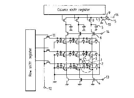
In Figure 1, a unit picture cell of the array
comprises a photocon~ersion e]ement or sensor twhich
is a bipolar transistor type device as disclosed in
EP-A-0132076) T. The base of the sensor T is
capacitively coupled to a control electrode, and this
: :
: . -
:-
'
coupling i~ represented by a capacitor C.
Additionally, the base is ~oupled to a P-channel FET
(e.g. a MOSFET) M. Each row of the array oP sensors
has a common horizontal drive line 2, connected to the
capacitor electrode and the gate of the FET M of~each
cell. Each column of the array has a common vertical
output line 3, connected to the emitter of each sensor
T. Each vertical output line 3 is connected to ground
through a respective FET 4, for resetting the vertical
output line 3. Each vertical output line 3 i5 also
connected to a respective capacitor 5 for storing
signals output from a sensor T onto the output line 3,
th.rough a respective FET 6. Each storage capacitor 5
is connected to a common horizontal output line 7
through a respective FET 8, and the common horizontal
output line 7 provideY an input to an amplifier 9.
The common horizontal output line 7 is also connected
to ground through an FET 10~
For controlling the operation of the device, each
horizontal : drive line 2 is connected through a
respective:FET 11 to a te inal 12 for supplying dri.ve
pulses, and the rows of the array are selected by
outputs from a row shift register which turn on the
FETs 11 in turn. Control pulses to a terminal 13
.
20~8~67
-- 7
turn on the FETs 4 to ground the vertical output
lines 3, and control pulses to a terminal 14 to turn
on the FETs 6 to connect the vertical output lines 3
to the storage capacitors S. Outputs from a column
shift register selectively turn on the FETs-- 8 to
connect the selected storage capacitors in turn to the
common horizontal output line 7. Control pulses to a
t~ inal 15 turn on the FET 10 to ground the
horizontal common output line 7 to reset it. The
photoconversion output signal from the device is
provided from the amplifier 9 to an output te in~l
16.
As can be seen in Figure 1, an additional FET M is
provided at one end of each row, so that an FET M is
present at each end of each row. Except at each end of
each row of the array of sensors T, the tWG main
électrode regions (source and drain) of the FET M of
~ each cell are connected respectively to the base of
the sensor T of the same cell and the base of the
sensor T of an adjacent cell. At each end of each
row, the FET connects the base of a sensor T to a
llne leading to ground. Thus, when a horizontal drive
line 2 turns on the FETs of one row of sensors, the
bases of all the sensors in the row are connected
,
. , ~: ;. . . . .
- :
.. .
.. . . .
- .
2 0 ~ 7
through the FETg M to grvund The additional FET M in
each row can be omitted, in which case the line of
FETs is connected to ground at one end only.
S Figure 2 illustrates waveforms of the signals applied
to the terminals 12,13 and 14. Throughout this
specification the convention will be used that the
waveform applied to a terminal will be indicated by
followed by the number of the terminal.
During the accumulation period, when the
photoconversion device is exposed and charges are
accumulated in the base of each sensor T in accordance
with the amount of light incident on the sensor, the
relevant row of the array of sensors is not selected
by the row shift reglster. If none of the rows is
being read or refreshed ~12 is at ground, ~13 is high
to connect the vertical output lines to ground, and
~14 is low to isolate the vertical output lines from
the storage capacitors 5. When a row is selected for
reading and refreshing, the row shift register turns
on the corresponding FET 11.
~: :
..
20~8~7
_ 9 _
For ~he reading oper~tion ~13 goes low to isolate ~he
e~itters of the sensors T and the vert.ical output
lines 3 from ground, and ~14 goes high to connect the
emitters and the vertical output lines 3 to the
storage capacitors 5. ~12 goes high sufficiently to
raise the potential of the bases of the sensors T in
the selected row through the action of the capacitor C
to turn on the transistor type sensors T so that an
output signal corresponding to the quantity of charges
stored in the base region is provided through the
emitter region to the respective vertical output line
3 and is stored on the respective storage capacitor 5.
The positive pulse of ~12 firmly turns off the FETs M,
so that the base voltage level is not influenced by
the ground connection through the FETs M during
read-out. Subsequently, the column shift register
turns on the PETs 8 in turn to read out the signals
'from the storage capacitors 5 to the common horizontal
:output line 7 and the amplifier 9. :~
For a refreshing operation, 013 goes high and ~14 goes
low to isolate the emitters and the vertical output
lines 3 from the storage capacitors 5 and connect them
again to earth, and ~12 goes sufficiently low to turn
on the P-type FET M. The low-going pulse of ~12 will
... .
,~ , -
~ . ~, -
2~8~67
-- 10 --
initially bias the base of each sensor to turn if off,
and then the base of each sensor will become grouncled
through the FETs M, with charges flowing into or
flowing out of the base region depending on the
quantity of charge carriers which have been
accumulated during the accumulation period. Thi.s
provides the so-called complete refresh operation, in
which the base of each sensor T of the selected row is
set to a common potential.-
Next, ~12 goes high once again to turn off the P-type
FETs M and forward bias the base of the sensor T
relative to the emitter by the action of the capacitor
C. The emitter l. ~ins connected to ground through
the FET 4. This provides the so-called transient
reset, during which charges stored in the base region
are L~ -lved through the emitter region. Because the
base of each~ sensor T of the selected row has~been
set to a standard level through the FETs M during the
complete reset operation, all of the base regions of
the sensors in the row are set to a common refresh
level at the end of the transient refresh operation.
2~g~67
~12 then returns to the grourld level to begin the
next accumulation period, and the row shLft register
can turn off the relevant FET 11 to de~select the
row.
As will be appreciated by those skilled in the art, it
is possible to provide an alternati~e construction in
which a first set of horizontal drive lines controlled
by a first row shift register are used exclusively for
read out, and a second set of horizontal drive lines,
controlled by a second row shift register, are used
exclusively for refreshing, and such an arrangement is
illustrated schematically in Figure 3.
:
'15 In Figure 3, read out is controlled by a read out row
shift register 30 with a timlng tR and refresh is
controlled by a refresh row shift register 31 with a
timing tC. By controlling the period between the
drive timing tR of the read out row shift register and
the drive timing rC of the refresh row shift register,
the accumulation period for each sensor can be
controlled, providing the so-called electronic shutter
function. In this Figure, a column shift register 32.,
the photoconversion array 33 and the output amplifier
34 are also illustrated schematically.
:~
:
2~,8L~67
- 12 -
The arrangement of Figures 1 and 2 has the advantage
that, by providing a common con~rol line for ~he
capacitor electrode controlling the base through
capacitor C and the gate of the FET M, the FET M is
automatically driven reliably into the off state
during read out and the transient refresh operation~
However, the total safe voltage range between the
highest voltage and the lowest voltage which may be
applied to the horizontal drive lines 2, is defined by
the characteristics of the components of the
photoconversion device, and particularly by their
-xi withstand voltages. Consequently, the fact
~hat the horizontal drive lines 2 must go negative in
order for the complete refresh operation to be carried
out llmits the -~i positive voltage which can be
applied during transient refresh and read out. This
limits the extent to which the transistor type sensor
~element T can be turned on, 60 that the read out
signal l' -in~ relatively low and the O~i lm output
signal when the sensor is saturated by bright light is
relatively small. Additionally, the circuit for
supplying the drive waveform ~12 must be relatively
compllcated as three different levels are required for
this waveform.
In the d~vices of Figures 1 to 3 a prob]em can arise
when a still picture is being taken, for example if
the device is used in a still video carnera,
particularly when a still picture is required of a
S moving object. Because each row is read and refreshed
at a different time, the accumulation periods for
different rows are provided with slightly different
timings. This results in an image distortion. This
lmage distortion can be eliminated by providing a
mechanical shutter which is opened after all of the
rows have been refreshed and is closed before any of
the rows are read~ However, in this case there may
still be an undesirable dark current during the time
taken to read and refresh all of the picture cells.
'15
The present invention in its various aspects seeks to
solve or reduce the various problems discussed above
or provide ; ~lOV~ ts over the arrangements
described.
~0
In the present specification reference is made to main
electrode regions and control regions of devices. As
will be well~understood by those skilled in the art,
most electrical components have first and second main
terminals, such as the two ends of a resistor, and the
.
., : '
20~8~7
- 14 -
two termina]s of a diode or a capacitor, and in the
case of three terminal devices such as transistors~
SCRs and TRIACs, a voltage or curren~ between the two
main terminals is influenced by a signal at a control
terminal. Thus, a bipolar transistor has a main
current path between its collector and its emitter,
which are main electrode regions, and the base is a
control region, and an FET has a main current path
between the source and drain, which are main electrode
regions. A double-emitter transistor will have two
main current paths, one for each emitter.
According to a first aspect of the present invention
there is provided a photoconversion device in which a
reset switch means is turned on to refresh a
photoconversion element by varying the voltage at a
main electrode of the switch means, preferably while
~eeping the voltage at a control electrode constant.
The present invention also provides a control circuit
for a photoconversion cell comprising a connection for
a main tq i n~ 1 of a refresh switch means of the cell
and means for applying a voltage to the connection for
turning on the switch means. The invention also
provides a method of refreshing a photoconversion
element by turning on an associated refresh switch
' ~
2~4~7
- 15 -
means by applying a turn on ~oltage to a main terminal
of a refresh switch means.
In an embodiment, the reset switch means such as FET M
is turned on by applying an appropriate voltage to a
main terminal rather than by varying the voltage
applied to a control terminal, thereby avoiding the
need for the refresh control pulse to be applied via a
horizontal drive line. In this way, the drive line
can provide a greater read pulse voltage without
exceeding the safe or stable operating range of the
apparatus.
In another aspect of the present invention storage
regions of photoconversion elements of a
photoconversion device having an array of elements are
connected to a standard voltage for resetting or
lnjecting carriers under at least some conditions of
the storage region at the same time for elements of a
plurality of rows of the array, and preferably at the
same time for all the elements in the array. The
present invention encompasses a device operating in
thLs manner or having means to operate in this manner,
a control circuit for a plurality of elements having
:
.: . . '
'' ~ ' ' ' ,
. ' .
2 0 Ll 8 l'l 6 7
~ 16 -
means to control them in this manner, and a method of
operating the device in this manner.
In another aspect of the present invention a
photoconversion element in which charges are stored in
a control region is refreshed or reset by applying a
refresh or reset voltage to a main electrode region of
the element so as to forward bias the elemen~ and
refresh or reset the control region through the main
electrode region. The present invention provides a
photoconversion device operating in this manner or
having means to operate in this manner, a control
circuit for a photoconversion element having means to
refresh or reset it in this manner, and a method of
re~reshing or resetting a photoconversion element in
this manner.
~n another aspect of the present invention reset or
refresh of a control region of a photoconversion
element through a main region of the element is
carried out sLmultaneously for elements in a plurality
of rows in a two~ n~ional array of such elements,
and prefersbly at the same time for all the elements
in the array. The invention provides a device, a
control circuit and a method using this concept.
2 ~ 7
In anot}ler aspect of the present invention the reset
or refresh opera~ion of photoconversion elements in a
plurality of rows of a two-dimensional array of
elements, and preferably all of the elements in the
array, is terminated simultaneously. The invention
encompasses a device, a control circuit and a method
using thls concept. This concept permits an
electronic definition of the beginning of the exposure
period without requiring different parts of the array
to have different exposure period timings.
In another aspect of the present invention a read out
terminal of a photoconversion element is held at a
first leveI during a period in which charge is
accumulated on a control region in response to
incident light and is brought to different level
before a read out period, the levels being chosen 50
that there is a voltage for the control region such
that charge will flow to the read out terminal when it
18 at the level provided during the accumulation
period but charge will not flow to the read out
te ;n~l when lt is at the voltage level selected for
the read out period. The invention includes a device,
a control circuit and a method using this concept.
2S This concept enables the ~i amount of charge
.. . .
' - ; ' ~ .
2 0 ~ 7
which can be stored in the control region if bright
light is incident on the photocon~ersion element to be
limited to a level ~hich provides a margin of safety
against the element influencing a signal read onto a
common read out line from another element, thereby
resisting a ~blooming~ effect of bright light exposure
on one photoconversion element.
Embodiments of the present invention, given by way of
non-limiting example, will now be described with
reference to the accompanying drawings, in which:
Figure 1 shows a photoconversion device illustrated
for the purpose of explanation;
~15 ''
Figure 2 shows a control waveform regime for the
operation of the device of Figure l;
.,
Figure 3 illustrates schematically a device having
separate read out and refresh row shift registers;
Figure 4 shows schematically a camera arrangement in
whLch embodlments of the present invention may be
used;
: .
-
.~
2~8~7
- 19
Figure 5 shows a photoconversion device according to a
first embodiment of the pre~ent invention;
Figure 6 shows a control waveform regime for the
device of Figure 5;
Figure 7 shows a photoconversion device according to a
second embodiment of the present invention;
Figure 8 shows a photoconversion device according to a
third embodiment of the present invention;
Figure 9 shows a control waveform regime for the
device of Figure 8;
Figure lO shows an alternative control waveform regime
for the device of Figure 8;
., ~ .
Figure 11 shows a photoconversion device according to
:a further embodiment of the present invention;
Figure 12 illustrates a control waveform regime for
the device of Figure 11;
.- ~ : .
.
.
_ 20 -
Figure 13 illustrates an alternative control wavefvrm
regime for the device of Figure 11; and
Figure 14 illustrates a control waveform regLme for
the read out period for any of the illustrated
photoconversion devices.
Embodiments of the present invention may be used in a
camera system such as is illustrated schematically in
Figure 4. Light from a scene passes through a lens
system 100 and a mechanical shutter 200 to be imaged
on a photoconversion element array of a
photoconversion device 300. The opening and closing
of the mechanical shutter 200 can control the exposure
t~me of the image on the photoconversion device 300,
:although the effective exposure period can also be
influenced by the optical shutter effect of the sensor
reset timing of the: photoconversion array as has
already been mentioned. A sequential output:signal
from the photoconversion~ device 300 is processed in a
signal processing cîrcuit 400, and is stored in a
storage medium 500 such as a semiconductor memory or a
floppy disc. The operations of the components are
controlled by a system controller 600.
~ Photoconversion devices embodying the present
~: :
::
: .
, ~ ~
~- ' ~: ,
' '
2~8~
- 21 -
invention can be used as the photoconversion device
300.
Figure 5 illustrates a first embodiment of the present
invention. Many parts of the photoconversion dévice
shown in Figure 5 are the same as in Figure 1, and
such parts have been given the same reference numeral.
However, as compared with Figure 1 the device of
Figure 5 comprises a second FET 17 for each row, also
controllable by the row shift register. The main
electrode regions (source and drain) of the FETs M of
the cells, which are used in the complete reset
operation, are connected to the bases of adjacent
sensors T of the row, as in Figure 1, except at the
lS ends of the rows. At the ends of the rows, the FETs M
are not connected to ground, but are instead connected
to the output of respective emitter followers 18 which
are provided for each row. The bases of the emitter
followers 18 are connected through the respective FETs
17 to a ter~inal 19. Thus, when the row shift
register selects a given row, the source of the reset
switch FET M of the end cell is connected to a voltage
set by the waveform at the terminal 19. The emitter
follower 18 ensures that a high current can be
.
.. . .
:
.
2~8~67
- 2~ -
sustained. In this en~bodi.ment, the additional FET M
at the end of eacll row i8 omi,tted.
The waveforms at the control t,erminals 12,13,14,19 in
the read and refresh operations of the device of
Figure 5 are shown in Figure 6. The reading operation
is similar to the operation described with refexence
to Figure 2 for the device of Figure 1~ Thus, ~13
goes low ta separate the vertical output lines 3 from
ground, and 014 goes high to connect the vertical
output lines 3 to the storage capacitors 5. ~12 goes
high, transmitting a high voltage pulse to the
horizontal drive line 2 of the selected row through
the FET 11 which has been turned on by the row shift
'15 register. The row shift regis~er will also have
turned on the FET 17 for the selected row, but ~19
~ in~ low so that the source of the FET switch M of
~~he end cell is at earth as in the arrangement of
Figure 1. The high voltage pulse on the horizontal
drive line 2 is transmitted through the capacitors C
of each cell of the selected row to the bases of th~
bipolar transistor type sensor elements T, which turn
on. Accordingly, read out signals are placed on the
vertiaal output lines 3 and are stored in the storage
capacltors 5.
- ,
,
.' ~ .
2~8~7
- 23 -
For the complete refresh operation, by which ~he bases
of the sensors T are set to a predefined voltage
level, ~12 returns to ground, but does not go
negative as in the device of Figure 1. Instead, ~19
S goes positive, raising the source voltage of the end
reset FET M, through the emitter follower 18. Thus,
the FET M turns on by having its source voltage raised
instead of by having its gate voltage lowered. When
it has turned on, it applies the voltage from terminal
19 to the base of its associated sensor T, and also to
the source of the next reset FET M. Consequently, the
next reset FET M turns on in the same way, and in this
manner all of the reset FETs M are turned on and the
bases of all of the sensors T in the selected row are
reset b~ the voltage at control terminal 19 through
the emitter follower 18. This is the complete refresh
operation.
.,
At the end of the complete refresh operation ~19 goes
low again and the transient reset operation is carried
out. This is similar to the transient reset operation
of Figures 1 and 2. ~13 i5 high to connect the
emitters to ground through the vertical output lines
3, and ~12 goes high to forward bias the bases of the
sensors T relative to the emitters, so that the
.
2 0 ~ 7
~ 24 _
quantity of stored charg~ falls to the prede~ined
level.
Subsequently, 012 falls again, reverse biasing the
base-emitter junction, and the next accumulation
period begins.
Because the compl~te refresh operation is carried out
by driving the sources of the reset switch FETs M high
from te in~l l9 rather than by driving their gates
low from te in~l 12, the voltage on the horizontal
drive lines 2 does not need to go negative, and
accordingly a higher positive read out control voltage
can be provided without the ~otal voltage range on
i5 the horizontal drive line 2 being excessive. Thus, a
higher level read out signal can be obtained.
Additionally, the waveforms at each of the terminals
~2~19 varies only between two voltages, and so the
control circuitry may be less complex than the
clrcuitry required to provide the three level waveform
at ~ i n~ 1 12 in the arrangement of E'igures 1 and
2.
': , :
.. '~ , , '
2 ~ 7
- 25 -
Figure 7 fllustra-tes a second embodiment of the
present invention. In this embodiment, the ~nd FET
transistors M of each row are connected together, and
are connected to the output of a single common emitter
follower structure 18. Additionally, each hori~ontal
drive line 2 is connected to ground through a
respective FET 20, which is controlled by a common
control te.rminal 21.
In this embodiment the complete refresh operation for
all the cells of the two-dimensional array is carried
out simultaneously. A high voltage is applied to
t~ in~l 21, to connect all of the horizontal drive
lines 2 to ground independently of the operation of
the row shift register. In this condition~ the high
voltage is applied to control te i nal 19 to raise the
source t~ in~l S of the refresh FETs M of the end
: cells of each row through the emitter follower
structure 18. In this way, the complete refresh
operation is carried out as described with reference
to Figures 5 and 6, except that all of the cells are
freshed in a single complete refresh operation.
Subsequently, the transient refresh operation may be
carried out for each row in succession, in accordance
.
'
2~8~7
- 26 -
with the selection by the row shift register, in the
manner already described.
This embodiment has the advantages of the embodiment
of Figure 5, and additionally less time is required
for the complete refresh operation since only a single
operation is required to provide complete refresh for
all rows. This embodiment is usable in a still video
camera, for example.
Figure 8 shows a third embodiment of the present
invention. This embodiment is similar to the
embodlment of Figure 7, except that the FETs 20 do not
connect the horizontal drive lines 2 to ground, but
instead connect them to a further control te in~l 50.
With this arrangement, it is possible to connect all
of the horizontal drive lines 2 to the te in~l 50
simultaneously, and provide a high pulse on the
te inAl 50 so that a transient refresh operation can
be carried out simultaneously for all of the cells of
the array.
, . .
As will be appreciated by those skilled in ~he art,
the provision of the te inal 50 also means that the
complete refresh operation can be carried out
.. ~ .
.
~.- . :
~. , .
, ~,, ., .;, ,
2~8~67
- 27 -
simultaneously for all ~he cells of the array even if
the end F~ETs M of each row are connected to ground as
in Figure 1 and the emitter follow~r arrangement 18
and the terminal 19 are not provided. A simultaneous
complete refresh operation could in this casë be
provided by connecting all of the horizontal drive
lines 2 to the terminal 50 through the FETs 20, and
applying a negative voltage to the terminal 50.
However, this is less advantageous than the structure
of Figure 8, since it means that the horizontal drive
line 2 must carry a negative voltage at times, thereby
reducing the -~i positive voltage which can
safely be applied to the line.
lS Figure 9 is~a timing diagram for the control waveforms
for the embodiment of Figure 8. Figure 9 shows a
control regime in which two separate transient refresh
operations are carried: out after the complete refresh
operation.
According to FLgure 9, at an initial period T0 the
shutter may be either open or closed. ~13 is high,
so that the emitters of the photoconversion element
sensors T are connected to ground. It is particularly
desirable to connect the emitters to ground if the
~ ;' ; ~ ' ' , : ',
~'.~ , .
.. . .
2 ~
- 2~ -
shutter is open, in case strong liyht is incident on
the photoconversion device so that a large quantity of
charges are stored in the base of the sensors 1'. In
this case, the grounding of the emitters enables
excessive charges in the base to drive the
base-emitter junction into forward bias, and the
excessive charges axe then led off to ground through
the emitter. If the emitter is not grounded, the base
voltage can continue to rise in bright light, taking
the emitter ~oltage up with it. In this case, there
is a possibility that during the complete reset
operation the base will be set to a voltage below the
emitter voltage, and it may then become difficult to
forward bias the base-emitter junction during a
subsequent transient reset operatlon, so that the
transient reset operation does not correctly reset the
base voltage.
The complete refresh operation is carried out in
perlod Tl. ~21 goes high, turning on the FETs 20 and
connecting the horizontal drlve lines 2 to the
terminal S0. The terminal 50 stays at ground~ ~19
goes high, and this voltage is applied through the
emitter follower 18 to the refresh FETs M, turning
-
.
29 -
them on, so that the bases of the sensors T are
refreshed in the manner described above.
Following the simultaneous complete refresh in period
S Tl, ~19 and 021 go low and during period T2 ~1 3 goes
high to reconnect the emitters of the sensors T to
ground. This provides a first simultaneous tr~nsient
refresh operation.
In period T3, a second simultaneous transient refresh
operation is carried out. ~21 goes high again to
connect the horizontal drive lines 2 to the te i n~ 1
50, and ~50 goes high to drive the bases of the
sensors T high through the capacitors C. Pre~erably,
~21 is higher than p50 during this period, to avoid
the high voltage on the terminal 50 adversely
affecting the turn-on characteristics of the FETs
'~0.
At the end of the second simultaneous transient
refresh perlod T3, the charge accumulation period
(exposure period) T4 begins, and the shutter is opened
if it was not already open. If the shutter was
already open, the end of the second simultaneous
transient refresh period T3 begins the exposure period
-
:: :
'
2~48~67
- 30 -
through the so-called electronic shutter effect. As
is shown in Figure 9, the exposure period T~ is ended
by the closu~e of the mechanical shutter ~00/ and
subse~uently the photoconversion signals are read out
during a read out period T5 in which the voltage at
terminal 12 is high and the read out operation is
controlled by the row shift register and the column
shift register as will be apparent to those skilled in
the art.
In this embodiment, the exposure period may be started
by the electronic shutter effect of the end of the
second simultaneous transient refresh period T3, such
that the timing of the exposure period is the same for
all rows because this refresh operation is
simultaneous for all rows.
~~igure 10 shows an alternative control signal regime
for the photoconversion device of Figure 8. In this
control regime only a single transient refresh
operation is carried out, in period T3, and period T2
i6 : eli inated~ The operation of the device in
accordance with Figure 10 is substantially ~he same as
its operation in aocordance with Figure 9, excep~ that
in Figure 10 at the end of the simultaneous complete
,
: . ~ , .
., , . ,.
. . .
.. , ~,, ~ . , .
': .
2 ~
- 31
refresh period T1 the waveform ~21 remains high, and
then in period T3 ~13 and ~15 both rise to a high
level to carry out a sinyle simultaneous transient
refresh operation.
s
In the control regimes of Figures 9 and 10, all of the
refresh operations are simultaneous for all rows of
the device. Consequently, the time required for the
refresh operations is relatively small, which assists
in providing high speed operation of the device.
As mentioned above, if very bright light is incident
on a photoconversion element before the refresh
operations are carried out, the emitter voltage of the
element may rise to a high level compared with the
level of the base following the complete refresh
operation, such that the base-emitter junction is not
'forward biased, or is not sufficiently ~forward biased,
during a subsequent transient refresh operation.
Additionally, the arrangement of the control t~ in~l
19 and the emitter follower 18 means that in the
complete refresh operation the base terminals of the
sensors T will be set to a voltage higher than ground.
The positive pulse applied to the base voltage through
the rapacitor C frr transient reflesh drives the base
. ' , .
2~8~7
- 32 -
voltage even higher, and there i9 a possibility that
this might lead to undesirably large currents flowing,
at least for a brief period, during the transient
reset operation. The operation carried out during
S period T2 assists in reducing these potential
difficulties, by setting the emitter voltage to ground
before the positive pulse is applied to the base for a
transient refresh operation. However, a further
embodiment of the present invention, illustrated in
Figure 11, is preferred for reducing these
difficulties.
In Figure 11 the device of Figure 8 is further
modified by adding FETs 4', controlled by control
te inAl 13', in parallel with FETs 4, so that the
vertical output lines 3 may be connected to ground
through the FETs 4 or alternatively to a negative
voltage -Vvc through the FETs 4'. A first control
xegime for this device is shown in Figure 12. This
control:regime is generally similar to the regime of
Figure 9 for the device of Figure 8, except for the
period T2.
.
, :. -
. ~..
' . - :
:,'' ~ .
2~48~67
- 33 -
n Figure 12 during period T2 ~13 remains low, while
~13' goes high, so that for the first simu1taneous
transient refresh ope~ation the emitters o~ the
sensors T are connected to the voltage -Vvc, which is
S below ground level. Therefore the emitters, and
through them the bases, are pulled down strongly. In
this way, the voltage on the base of each cell is
reduced to be substantially ground level after the end
of the first transient refresh operation in period T2,
so that during the second transient refresh operation
in period T3 a high instantaneous current is avoided
even though the base is set to a voltage significantly
above ground level during the complete refresh
operation. Additionally, the emitter voltage is
lS reliably brought to a low level before the second
transient refresh operation is carried out, even if
bright light is incident on the photoconversion
element T so that the emitter was prevlously at a high
level. Thus, the base-emitter junction can be
reliably forward-biased during the second transient
refresh operation in period T3.
In the arrangements of Figures 8 and 11 it is
preferred that the voltage applied to the ter~inal S0
for a transient refresh operation, shown as VA in
34 -
Figure 12, is less than the voltage applied to the
termi.nal 12 for read out, shown as V~ in Figure 12.
Voltage VA sets the extent to which the base~emitter
juncticn is reverse biased at the beginning of the
S exposure period, and by making voltage VB bigger than
voltage VA the bipolar transistor type photoconversion
element T can be relatively strongly forward biased
during read out, so that a suPficient forward bias for
an effective hi.gh speed read out operation can be
achieved regardless of the hfe value of the
photoconversion element T.
Figure 13 shows an alternative control regime for the
device of Figure 11. In this regime, the second
lS transient refresh operation is carried out
sequentially for the various lines of the array,
rather than simultaneously, so that the currents
flowing during the second transient refresh operation
are lower. Accordingly, tP inal 50 is maintained at
ground level, and this terminal may be provided as a
direct ~connection to ground in the manner of the
device of Flqure 7.
,
~, '": ~ ,: .
: . .
, ~
.,, . : :
-, ~ ' ': .
. .
.
2~8~7
- 35 -
In Figure 13, the operations in periods T0, Tl and T2
are the same as .in ~igure 12. However, for the second
transient refresh operation ~21 and ~50 remain low,
and instead the control voltage VA for the second
transient refresh operation is provided in waveform
~12 while the row shift register provides row select
signals 0v2 to select each row of the array for
transient refresh in turn. During the second
transient refresh operation ~13 is high, connecting
the emitters of the sensors T to ground through the
vertical output line 3 and FETs 4.
Since the bases of the sensors axe set to a relatively
high voltage during the simultaneous complete refresh
operation r a current will tend to flow from each
,
sensor i -~iately its emittex is connected to ground.
Thus, if the sequential txansient refresh bperation of
~:eriod T3, in which a posit1ve pulse is applied to the
bases of the selected sensors T follows directly aftex
the complete refxesh operation, there will be a leak
current from the non-selected sensors T in add1tion to
a high cuxxent from the stxongly forwaxd biased
selected sensors T. This is avoided by the
pxeli inAry simultaneous txansient refresh opexation
during peri~od T2. Even if the base voltage is above
2 0 ~ 7
only 0.2 or 0.3 volts after the end of the
simultaneous transient reset operation of pe~iod T2, a
small leak current may flow from the emitters of
non-selected sensors during the sequential transient
reset operation in period T3. However, because the
emitters are set to a lower voltage through the FETS
4' during the simultaneous transient reset operation
than the emitter voltage set through the FETs 4 during
the sequential transient refresh operation, the
non-selected sensors are reliably turned off during
the sequent.ial transient refresh operation.
As previously mentioned, it is advantageous if the
read out control voltage VB is higher than the
transIent refresh control voltage VA.
Since the final refresh operation is sequential in
~igure 13, the mechanical shutter 200 is kept closed
during the refresh operation, and the exposure period
T4 begins when the mechanical shutter opens.
As shown in Figure 13, waveform ~13 is kept high
during the exposure period T4, so ~hat if one
photoconversion sensor is exposed to very strong light
and the cell is ePfectively saturated, the
.. , ~ . .
-. .. : . .- .
. ,
.~ ' '
''' -',~' ,.
,
2~8~'7
base-emitter junc~ion will become forward biased and
excess charges on the base will flow through the
emitter to ground. This redllces problems, such as
blooming, associated with strong light exposure of one
photosensor element. However, following the ending of
the exposure period ~4 by closure of the mechanical
shutter 200, the image signal is read out on the
vertical output lines 3 and a residual portion of the
current from a saturated photoconversion cell may be
added to the signal on its associated vertical output
line 3, so that blooming still occurs to some
extent.
This residual blooming effect can be avoided if pl3
is low during the accumulation period T4 and pl3' is
high. Thls means that the emitter voltage during the
accumulation period is lower than the emitter voltage
~or the last transient refresh operation in which a
positive base voltage is applied to the sensors. If
the emitter voltage during the accumulation period is
lower by a voltage VABV, the picture cells will
saturate at a lower base voltage kVABV (where k is a
coefficient for the change of base voltage with change
~ of emitter voltage~. By holding the emitter to this
lower voltage during the accumulation period, the
2 0 ~ 7
- 3~ -
maximum base t~oltage which can arise due to bright
light is r~duced. Following closure o~ the mechanical
shutter 200, the emitter voltage can be returned to
the voltage used during the sequential transient reset
S operation by turning off the FETs 4' and turning on
the FETs 4. In this way, a saturation voltage margin
is provided corresponding to kVABV, so that a
saturated picture cell ceases to be saturated after
the end of the exposure period, and therefore it does
not influence the vertical output line 3 during the
read out period. During the read out period T5 the
mechanical shutter is kept closed so that incident
light cannot affect the signal during this period, and
particularly strong light cannot create blooming.
By keeping the output ta i n~ 1 of the picture cell
(i.e. the emitter) at a standard voltage, in this case
ground,~for substantially the whole of the operation
cycle except for the read out period and the
simultaneous complete reset period, the reset current
can be ~in;~ised.
Figure 11 also shows the control signal terminals for
the row and column shift registers, and the waveforms
for the:e signals are included in Figu~es 13 and 14.
- : .
~ :
.
2 ~ 6 7
- 39 -
S is a vertical synchronising signal (i.e. a field
synchronising signal) for resettirlg the operation of
the row shift register. ~v2 carries the waveforms
which are output from the row shift register on the
selected lines to turn the FETs 11 on and off. ~V1
clocks the row shift register, so that each pulse of
~Vl changes the output line of the row shift register
which carries the waveform ~V2. The operation of
~ 1 and ~V2 can be seen clearly in Figure 13, in which
pulses of ~V2 are output on successive output lines
of the row shift register to enahle successive rows of
the array during the sequential transien~ refresh
operation, and clocking pulses of ~V1 change the
selected row. The signals ~HS, ~H1 and ~H2 provide
equivalent functions for the column shift register,
for the purpose of providing horizontal (row)
synchronisation, read out timing and column selection
signals within each row read out period.
Figure 14 shows a control regime for the read out
perlod T5. The read out period T5 is divided into
horizontal line periods, marked lH in Figure 14. Each
horizontal line period begins with a horizontal
blanking period marked HBLK. At the beginning of the
horizontal blanking period, in a period tO, ~V2 goes
,
2~8~7
- 40 -
low so that none of the hori~ontal drive lines 2 is
enabled, and ~V1 provides the clock pulse to select
the next row of the array. 5ubsequently ~VZ goes
high again to turn on the FET 11 for the next row of
the array. Also during the period tO, ~14 is high to
connect the storage capacitors S to the vertical
output lines 3 through the FETs 6, and ~13 goes on
briefly during the period to connect the vertical
output lines 3 $o ground through the FETs 4. Thus,
before the read out from the selected row begins,
residual signals are removed from the storage
capacitors 5 and the vertical output lines 3.
At the end of the period tO, ~Vl and ~13 go low
again, but ~14 L.- ~i n~ high, and in a period tl ~V2
goes high to connect the selected horizontal drive
line 2 to ter~in~l 12, and ~12 rises to the read out
voltage VB. Accordingly, the base region of each
sensor T of the selected row is raised through the
capacitor C, and the output signal is provided to the
respectlve vertical output line 3. Since ~14 is high,
the signal is passed to the respective storage
capacitor 5. At the end of the period tl, ~12 goes
low ending the read out operation from the cells, and
~14 goes low to lsolate the storage capacitors 5 from
- . :
~0~8~7
- 41 -
vertical output line~ 3. Therl, in period t2 the
operation of the column shi~t register is synchronised
by ~HS, and the si.gnals st,ored in the storage
capacitors 5 are read out in succe sion to the common
horizontal output line 7, the amplifier 9 and the
output terminal 16. This is done by turning on each
FET 8 in succession, by the application of waveform
~H2, with the FETs being selected in turn by the
clocking action of ~Hl. In between the energisations
of the FETs 8 to connect successive storage capacitors
5 ko the common horizontal output line 7, the common
horizontal output line 7 is earthed through FET 10 to
remove any residual signal. This may be done hy
applying the inverse of ~H2 to terminal 15, ag shown
in Figure ll, or in any other convenient way such as
by applying ~H1 to t~_ i n~ 1 15 or a specially
generated control signal.
As previously mentioned, the read out voltage VB
applied to the horizontal drive lines 2 is preferably
greater than the transient refresh voltage VA, to
ensure that a strong read out signal is provid0d from
the sensors T.
2~8~7
42 -
In order to reduce the instantaneous current which
flows when the sensors T are forward biased by a
positive pulse on the base during transient refresh,
the complete refresh voltage applied through emitter
follower arrangement 18 may be made as low as
possible, as an alternative to providing an operation
in which the emitters of the sensors T are pulled down
in what amounts to a preli in~ry transient refresh
operation. However, there is a limit to the extent to
which the emitter follower voltage can be lowered,
since the voltage must be sufficiently high to ensure
that the complete reset switch FETs M turn on.
Accordingly, the use of the preli in~ry simultaneous
transient reset operation during period T2 is
preferred.
The present invention has been described with
reference to embodiments given by way of example.
Modifications and alternatives will be apparent to
tho~e skilled in the art.
. -
.